
A 28 nm CMOS 10 bit 100 MS/s Asynchronous SAR ADC with Low-Power Switching Procedure and Timing-Protection Scheme


Abstract
:1. Introduction
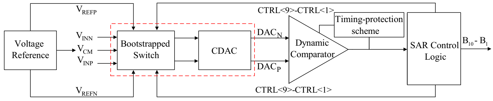
2. ADC Architecture
2.1. SAR ADC Architecture
2.2. Switching Procedure
3. Building Blocks Implementation
3.1. SAR Control Logic
3.2. Timing-Protection Scheme
3.3. Dynamic Comparator
3.4. Differential CDAC Array
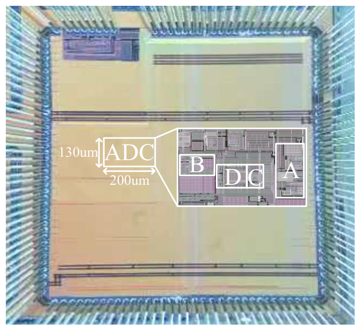
4. Measurement Results
5. Conclusions
Author Contributions
Funding
Conflicts of Interest
References
- Jimenez, O.; Lucia, O.; Urriza, I.; Barragan, L.A.; Navarro, D. Design and Evaluation of a Low-Cost High-Performance Σ-Δ ADC for Embedded Control Systems in Induction Heating Appliances. IEEE Trans. Ind. Electron. 2014, 61, 2601–2611. [Google Scholar] [CrossRef]
- Yoshioka, K.; Shikata, A.; Sekimoto, R.; Kuroda, T.; Ishikuro, H. An 8 bit 0.3-0.8 V 0.2-40 MS/s 2-bit/Step SAR ADC With Successively Activated Threshold Configuring Comparators in 40 nm CMOS. IEEE Trans. Very Large Scale Integr. (VLSI) Syst. 2015, 23, 356–368. [Google Scholar] [CrossRef]
- Roh, Y.-J.; Chang, D.-J.; Ryu, S.-T. A 40-nm CMOS 12b 120-MS/s Nonbinary SAR-Assisted SAR ADC with Double Clock-Rate Coarse Decision. IEEE Trans. Circuits Syst. II Express Briefs 2020, 67, 2833–2837. [Google Scholar] [CrossRef]
- Zhang, H.; Tan, Z.; Chu, C.; Chen, B.; Li, H.; Coln, M.; Nguyen, K. A 1-V 560-nW SAR ADC with 90-dB SNDR for IoT Sensing Applications. IEEE Trans. Circuits Syst. II Express Briefs 2019, 66, 1967–1971. [Google Scholar] [CrossRef]
- Liu, S.; Shen, Y.; Zhu, Z. A 12-Bit 10 MS/s SAR ADC with High Linearity and Energy-Efficient Switching. EEE Trans. Circuits Syst. I Regul. Pap. 2016, 63, 1616–1627. [Google Scholar] [CrossRef]
- Tseng, W.; Lee, W.; Huang, C.; Chiu, P. A 12-bit 104 MS/s SAR ADC in 28 nm CMOS for Digitally-Assisted Wireless Transmitters. IEEE J. Solid-State Circuits 2016, 51, 2222–2231. [Google Scholar] [CrossRef]
- Qiu, L.; Tang, K.; Zheng, Y.; Siek, L. A Flexible-Weighted Nonbinary Searching Technique for High-Speed SAR-ADCs. IEEE Trans. Very Large Scale Integr. (VLSI) Syst. 2016, 24, 2808–2812. [Google Scholar] [CrossRef]
- Kim, W.; Hong, H.K.; Roh, Y.J.; Kang, H.W.; Hwang, S.I.; Jo, D.S.; Chang, D.-J.; Seo, M.-J.; Ryu, S.-T. A 0.6 V 12 b 10 MS/s Low-Noise Asynchronous SAR-Assisted Time-Interleaved SAR (SATI-SAR) ADC. IEEE J. Solid-State Circuits 2016, 51, 1826–1839. [Google Scholar] [CrossRef]
- Li, M.; Chen, Y.; Ye, F.; Ren, J. A 100 MS/S 12-bit Coarse-Fine SAR ADC with Shared Split-CDAC. In Proceedings of the 2018 IEEE International Symposium on Circuits and Systems (ISCAS), Florence, Italy, 27–30 May 2018; pp. 1–4. [Google Scholar] [CrossRef]
- Okazaki, T.; Kanemoto, D.; Pokharel, R.; Yoshida, K.; Kanaya, H. A design technique for a high-speed SAR ADC using non-binary search algorithm and redundancy. In Proceedings of the 2013 Asia-Pacific Microwave Conference Proceedings (APMC), Seoul, Korea, 5–8 November 2013; pp. 506–508. [Google Scholar] [CrossRef]
- Rikan, B.S.; Seo, D.; Lee, K. A 10-b 10MS/s SAR ADC with power and accuracy control of the comparator. In Proceedings of the 2015 International SoC Design Conference (ISOCC), Gyungju, Korea, 2–5 November 2015; pp. 225–226. [Google Scholar]
- Haenzsche, S.; Höppner, S.; Ellguth, G.; Schüffny, R. A 12-b 4-MS/s SAR ADC with Configurable Redundancy in 28-nm CMOS Technology. IEEE Trans. Circuits Syst. II Express Briefs 2014, 61, 835–839. [Google Scholar] [CrossRef]
- Guerber, J.; Venkatram, H.; Oh, T.; Moon, U. Enhanced SAR ADC energy efficiency from the early reset merged capacitor switching algorithm. In Proceedings of the 2012 IEEE International Symposium on Circuits and Systems (ISCAS), Seoul, Korea, 20–23 May 2012; pp. 2361–2364. [Google Scholar]
- Veendrick, H.J.M. The behaviour of flip-flops used as synchronizers and prediction of their failure rate. IEEE J. Solid-State Circuits 1980, 15, 169–176. [Google Scholar] [CrossRef]
- Kobayashi, T.; Nogami, K.; Shirotori, T.; Fujimoto, Y. A current-controlled latch sense amplifier and a static power-saving input buffer for low-power architecture. IEEE J. Solid State Circuits 1993, 28, 523–527. [Google Scholar] [CrossRef]
- Li, D.; Liu, M.; Zhao, L.; Mao, H.; Ding, R.; Zhu, Z. An 8-Bit 2.1-mW 350-MS/s SAR ADC with 1.5 b/cycle Redundancy in 65-nm CMOS. IEEE Trans. Circuits Syst. II Express Briefs 2020, 67, 2307–2311. [Google Scholar] [CrossRef]
- Moon, K.; Jo, D.; Kim, W.; Choi, M.; Ko, H.; Ryu, S. A 9.1-ENOB 6-mW 10-Bit 500-MS/s Pipelined-SAR ADC with Current-Mode Residue Processing in 28-nm CMOS. IEEE J. Solid-State Circuits 2019, 54, 2532–2542. [Google Scholar] [CrossRef]
- Zhang, S.; Cao, Y.; Ye, F.; Ren, J. A 10b 250MS/s SAR ADC with Speed-Enhanced SAR Logic and Free Time More Than a Half of Sampling Period. In Proceedings of the 2019 IEEE 13th International Conference on ASIC (ASICON), Chongqing, China, 29 October–1 November 2019; pp. 1–4. [Google Scholar]


| Temperature (°C) | Corners | ENOB(bit)@0.8V | ENOB(bit)@0.9V | ENOB(bit)@1.0V |
|---|---|---|---|---|
| −40 | tt | 9.09 | 9.27 | 9.17 |
| ff | 9.19 | 9.39 | 9.32 | |
| ss | 9.06 | 9.16 | 9.09 | |
| fnsp | 9.16 | 9.35 | 9.25 | |
| snfp | 9.08 | 9.22 | 9.14 | |
| 27 | tt | 9.24 | 9.43 | 9.33 |
| ff | 9.39 | 9.52 | 9.48 | |
| ss | 9.18 | 9.32 | 9.26 | |
| fnsp | 9.34 | 9.47 | 9.4 | |
| snfp | 9.19 | 9.36 | 9.31 | |
| 125 | tt | 9.15 | 9.29 | 9.21 |
| ff | 9.26 | 9.41 | 9.33 | |
| ss | 9.05 | 9.21 | 9.14 | |
| fnsp | 9.2 | 9.35 | 9.25 | |
| snfp | 9.12 | 9.26 | 9.16 |
| [16] TCAS-II 2020 | [3] TCAS-II 2020 | [17] JSSC 2019 | [18] ASICON 2019 | This Work | |
|---|---|---|---|---|---|
| Architecture | SAR | SAR | Pipe-SAR | SAR | SAR |
| Process (nm) | 65 | 40 | 28 | 28 | 28 |
| Supply (V) | 1.2 | 1 | 1 | 1.05 | 0.9 |
| Fs (MS/s) | 350 | 120 | 500 | 250 | 100 |
| Resolution (bit) | 8 | 12 | 10 | 10 | 10 |
| SNDR@Nyq. (dB) | 45.7 | 58.1 | 56.6 | 52.4 | 51.54 |
| ENOB (bit) | 7.3 | 9.36 | 9.1 | 8.4 | 8.27 |
| Power (mW) | 2.1 * | 1.9 | 6 | 3.23 | 1.1 * |
| FOM (fJ/c-s) | 38.1 | 24.1 | 21.8 | 38.2 | 35.6 |
| DNL (LSB) | +0.9/−0.6 | +0.96/−0.93 | +0.48/−0.32 | +0.96/−0.86 | +0.37/−0.44 |
| INL (LSB) | +0.7/−0.7 | +1.6/−1.08 | +0.67/−0.61 | +1.37/−1.02 | +0.48/−0.63 |
Publisher’s Note: MDPI stays neutral with regard to jurisdictional claims in published maps and institutional affiliations. |
© 2021 by the authors. Licensee MDPI, Basel, Switzerland. This article is an open access article distributed under the terms and conditions of the Creative Commons Attribution (CC BY) license (https://creativecommons.org/licenses/by/4.0/).
Share and Cite
Tang, F.; Ma, Q.; Shu, Z.; Zheng, Y.; Bermak, A. A 28 nm CMOS 10 bit 100 MS/s Asynchronous SAR ADC with Low-Power Switching Procedure and Timing-Protection Scheme. Electronics 2021, 10, 2856. https://doi.org/10.3390/electronics10222856
Tang F, Ma Q, Shu Z, Zheng Y, Bermak A. A 28 nm CMOS 10 bit 100 MS/s Asynchronous SAR ADC with Low-Power Switching Procedure and Timing-Protection Scheme. Electronics. 2021; 10(22):2856. https://doi.org/10.3390/electronics10222856
Chicago/Turabian StyleTang, Fang, Qiyun Ma, Zhou Shu, Yuanjin Zheng, and Amine Bermak. 2021. "A 28 nm CMOS 10 bit 100 MS/s Asynchronous SAR ADC with Low-Power Switching Procedure and Timing-Protection Scheme" Electronics 10, no. 22: 2856. https://doi.org/10.3390/electronics10222856
APA StyleTang, F., Ma, Q., Shu, Z., Zheng, Y., & Bermak, A. (2021). A 28 nm CMOS 10 bit 100 MS/s Asynchronous SAR ADC with Low-Power Switching Procedure and Timing-Protection Scheme. Electronics, 10(22), 2856. https://doi.org/10.3390/electronics10222856