1. Introduction
The continuing trend of rapid reduction in the transistor’s size is causing a large increase in the density of the digital IC, resulting in severe problems in placing low parasitic interconnects within the standard cells. This reduction of transistor size is essential as it would allow more transistors to be fit on a chip of the same dimensionality and help manufacture smaller electronics. Moreover, we are nearing the limit of transistor dimensionality reduction, making it increasingly difficult to keep up with the golden rule of the industry, i.e., Moore’s law [
1]. One potential solution to these problems is the three-dimensional IC layout structure, which can contribute to ultra-high-density ICs, leading to higher performance and lower overall power dissipation.
The evolution of the IC physical design first produced the 2.5D structure, which consists of an interposer layer, with individual die placed on top of it [
2]. This served as a steppingstone for the design of the 3D IC, which consisted of silicon die placed vertically on top of each other. The individual dies are referred to as tiers and they are made up of a silicon substrate, followed by a device layer with an interconnect layer on the top [
2,
3,
4]. The early 3D designs involved the tiers being fabricated separately and placed on top of each other and connected with the help of vertical interconnects called through-silicon vias (TSVs) [
5,
6,
7,
8,
9,
10,
11]. However, there were several disadvantages to the usage of TSVs compared to the utilization of the more recent technology of monolithic inter-tier vias (MIVs). The large pitch and size of the TSV results in high parasitic capacitance and resistance, and limits the density with which they could be placed. Conversely, MIVs are orders of magnitude smaller in comparison and comparable in dimensions to a regular inter-tier via, which is less than 100 nm in diameter [
12]. The monolithic IC is made by fabricating each tier sequentially instead of putting them together after fabrication, as done with TSV-based designs.
Significant work has been done on the monolithic 3D IC design in recent times, most of which contributed to developing various design concepts of 3D ICs. The studies in this field include developing a face-to-face stacked heterogeneous 3D IC structure [
13], exploring various microfluidic cooling mechanisms for 3D ICs [
14], studying recent developments in monolithic 3D ICs and the high density and performance benefits [
15], designing a logic-on-memory processor using monolithic 3D (M3D) IC techniques [
16], developing a design and testing system for M3D ICs [
17], comparing the TSV-based 3D structure with M3Ds [
18,
19], studying the effect of process variation on the performance of M3D ICs [
20,
21], and developing effective gate-sizing methods to boost circuit speed while considering intra-die process variation [
22]. Other related studies include repurposing various components of commercial 2D P&R tools to implement 3D ICs [
23,
24,
25,
26]. However, there are not many works related to the development of a complete RTL-to-GDS physical design flow for the M3D structure due to the unavailability of commercial EDA tools for M3D P&R implementation. The limited study in this area includes the design of an overall flow developed by H. Park et al. and the development of M3D logic by Y. Lee et al. [
27,
28,
29]. Our work involves an easy-to-use RTL-to-GDS design flow with custom-made tier partitioning algorithms. We analyzed the results obtained and compared them with that of related works and found a significant performance increase.
The major contributions of our work are provided below:
We developed two different tier partitioning systems named the minimum cut (min-cut) and analytical quadratic (AQ) algorithms and compared their results with related works. We also compared the results obtained on the same circuit with the AQ and min-cut partitioning algorithms.
We designed a complete RTL-to-GDS design flow that is easily implementable using existing EDA tools. We used the Design Compiler (DC) and the IC Compiler II (ICC2) tool from Synopsys® for performing the logic synthesis and P&R implementations, respectively.
We evaluated power dissipation results for two-to-five-tier designs for three benchmark circuits using two different tier partitioning algorithms and compared the results with a 2D layout. Finally, we examined the power dissipation reductions of increasing the number of tiers for different circuit types.
We presented the details of our overall design flow, our tier partitioning algorithms, and the P&R flow system in
Section 2. We reported and analyzed our results in
Section 3. Finally, we discussed our findings in
Section 4, and followed up with concluding remarks in
Section 5.
2. Methodology
2.1. Overall Design Flow
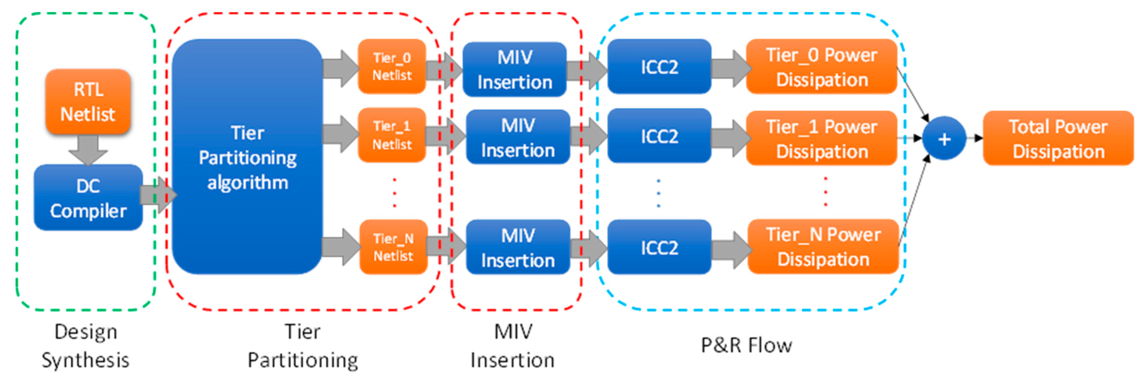
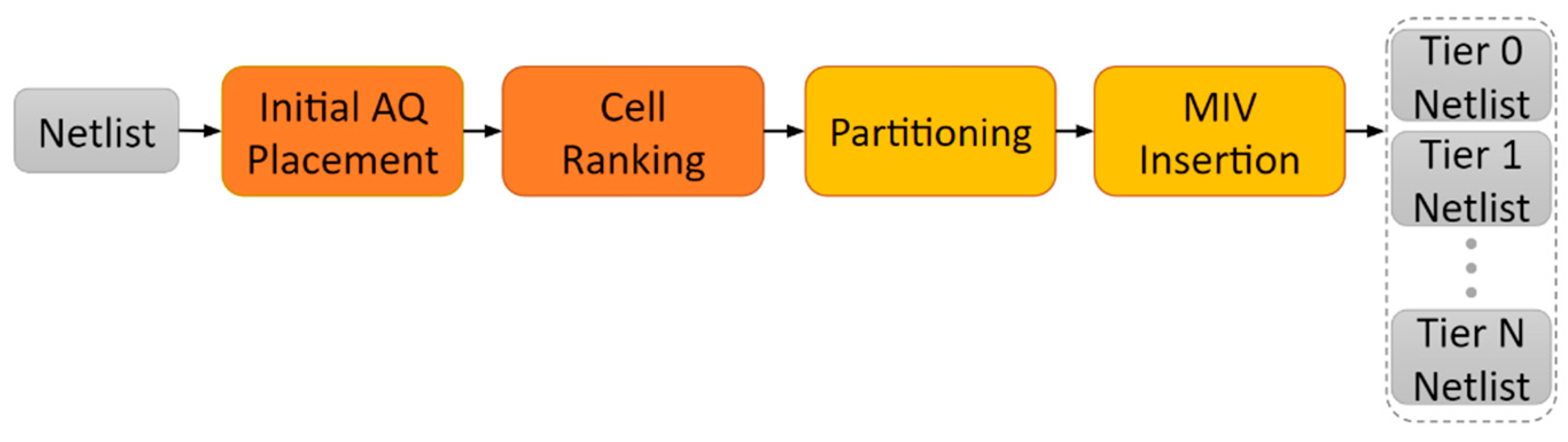
The pipeline for the overall design is shown in
Figure 1. The input of the system is a register-transfer level (RTL) netlist of the circuit. The Design Compiler tool from Synopsys
® was used to synthesize the circuit into a gate-level netlist, which was then passed into the tier-partitioning algorithm, which provides the individual tier netlists. The details of the tier-partitioning algorithm are discussed in
Section 2.2. The individual tier netlists are then passed to the Synopsys
® ICC2 tool for the placement and routing (P&R) flow. The power dissipation results of each tier are generated from the P&R design and added together to get the overall result of the 3D IC. Each tier in the design is of the same size and is reduced depending on the number of tiers in the 3D design. For example, if it is a two-tier design, then the total core area of each tier is half the size of the original 2D design.
2.2. Tier Partitioning
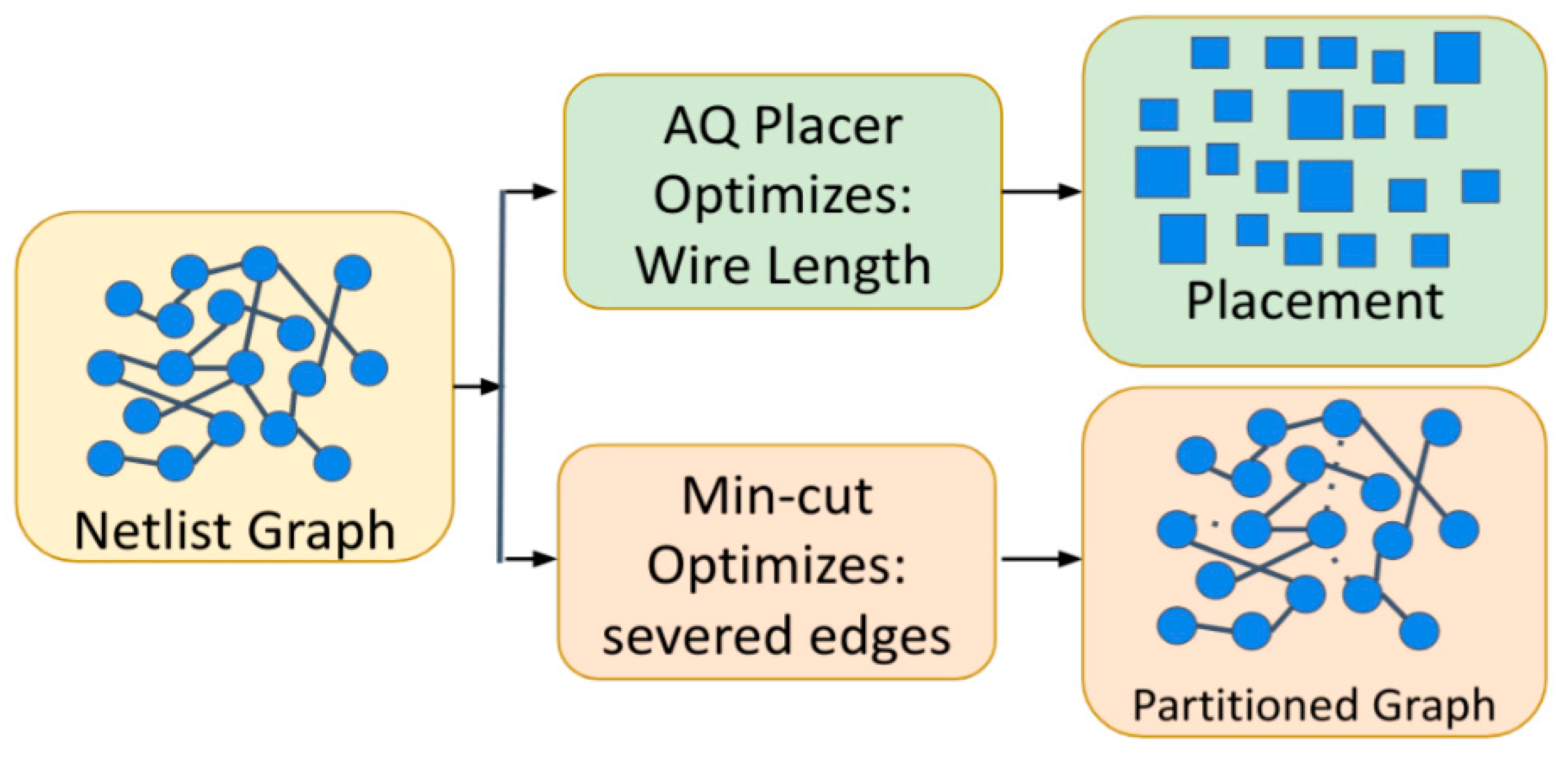
One of the main challenges of 3D IC design is partitioning the cells between the tiers. Intuitively, this step has the most impact on the final performance of the physical design since it explicitly affects the contents of each tier. A subpar tier partitioning, such as a random tier partitioning, would spread cells between arbitrary tiers and would disregard four main considerations: (1) their connections to different nets, (2) their location after placement, (3) the number of MIVs, and (4) the total area of the tiers after partitioning. In order to add these considerations to the tier partitioning step, this work implemented two approaches for tier partitioning; first, a minimum-cut algorithm, which has traditionally been used for partitioning the graph of the netlist, and second, an analytical quadratic algorithm, a novel algorithm that uses placement results in order to decide which cell belongs to which tier.
Figure 2 compares the two methods for tier partitioning and depicts that the main differences between the two algorithms are two-fold and are the type of the algorithm and the optimization goal of the algorithm. The min-cut algorithm directly performs on the netlist graph and optimizes the number of connections that would be severed due to partitioning. On the other hand, the placement algorithm works with netlist placement and optimizes the wire length between the placed cells. The implications of these two optimization strategies are discussed in the following subsections.
2.2.1. Partitioning Using the Minimum-Cut Algorithm
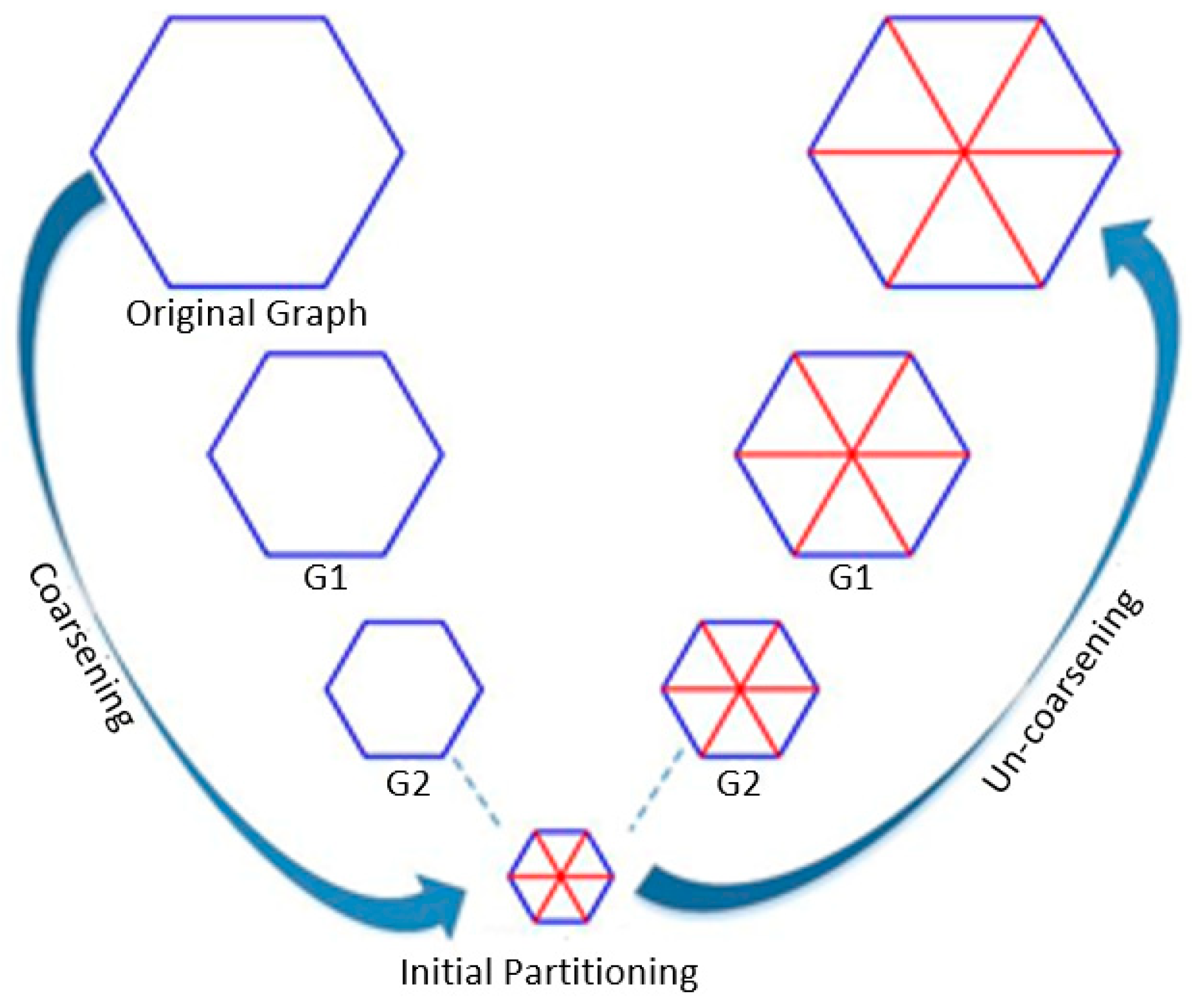
The min-cut algorithm was derived from the multilevel k-way partitioning graph (MKWPG) algorithm, which comprises three phases: coarsening, initial partitioning, and uncoarsening and refinement [
30,
31]. The process begins by coarsening the graph recursively until a graph with a small enough size is derived. More precisely, the input graph is replaced with a smaller graph version that is similar to the original graph but has fewer edges and nodes compared to the former. The process is repeated until a sufficiently small version of the graph is obtained that could be partitioned easily and quickly. After the coarsening phase is achieved, the initial partitioning begins to partition this small version of the graph to k parts. As this coarsest partitioned graph is somehow like the parent graph, it could be partitioned in the same manner. Lastly, in the uncoarsening step the original graph is partitioned via reversely repeating this process.
Figure 3 illustrates the three main steps of the MKWPG algorithm.
Inherently, a netlist is similar to a graph with nodes representing the gates, and edges representing the connections within the nets. Therefore, an algorithm such as min-cut can be leveraged to modify a netlist. Since the netlist is represented as a graph, the algorithm would directly work with the connections between the cells, which are represented as the edges of the graph. Therefore, using the min-cut algorithm would allow the tier partitioner to explicitly take into account the connections between the cells and the number of MIVs, which would replace the cut connections, heeding two of the main four considerations.
To implement the algorithm using a high-level language, the netlist graph needs to be represented by an adjacency matrix. The rows and columns represent vertices and the nonzero values in the adjacency matrix are edges where there are connections within the netlist. The breadth-first search (BFS) algorithm was used to compute the graph in the adjacency matrix. The matrix was then divided into k parts in a row-wise manner. These row blocks (k parts) were then processed where each row block representing a partition of the graph. The nodes were exchanged among the partitions repeatedly to balance the number of nodes between the parts and minimize the number of cut edges.
The min-cut partitioner starts by using Python to parse the gate-level Verilog circuit and convert it into a graph. The wires and the gates are represented as edges and nodes, respectively. Note that, since the sizes of the gate types are different, we weighed the converted gates based on the number of required transistors as described: inverter, buffer/NAND/NOR, AND/OR, XOR, and XNOR as 2, 4, 6, 12, and 14, respectively. Currently, we are focused on static CMOS logic, so the partitioner only works on static logic. This process is vital as the circuit size depends on the total number of transistors and not the total number of gates. We first convert/parse the Verilog circuit (including gates and wires) into a graph (including nodes and edges). During the conversion, we created a dictionary that has information about the Verilog circuit, e.g., gate type, gate name, gate location, wire direction, and number of transistors. We get the exact number of transistors for each gate type from the library since the library has all the gate information, including the number of transistors, which is very important to partition the circuit in an efficient way. Once the partitioning is done, we convert the partitioned parts back to partitioned circuits.
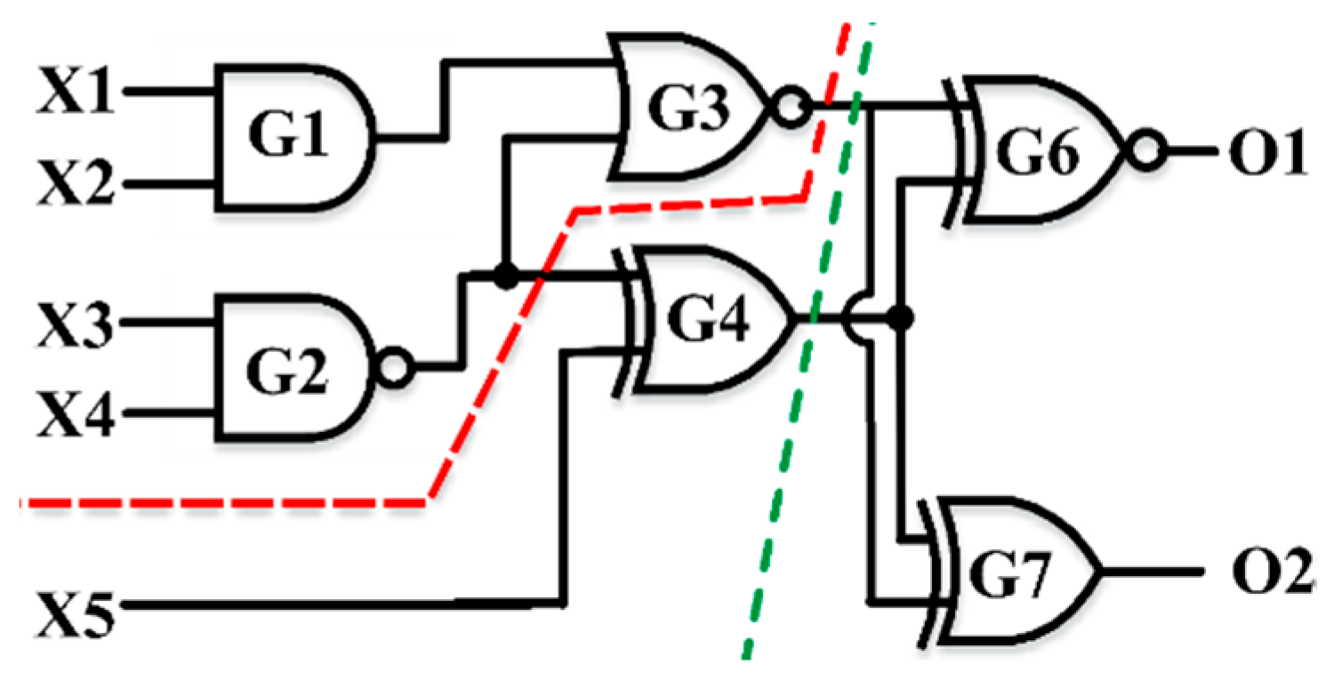
To clearly explain this, we use the small circuit shown in
Figure 4, which has six gates. If we partition the circuit into two parts without weighing the gates based on the gate type, then the algorithm will partition the circuit, as shown with the red dotted line, in which each part will have three gates with two cut edges (wires) as a minimum. This makes the size of the right part (part 2) larger than the size of the left part (part 1) by about 2.7 times since the number of transistors in part 1 is 14, while it is 38 in part 2. However, if we weigh each gate type before converting to the graph, then part 1 will have 4 gates (26 transistors) and part 2 will have 2 gates (26 transistors), as shown by the dotted green line. Hence, the process allows us to partition the circuit into k parts with equal size and a minimum number of cut edges.
2.2.2. Partitioning Using Initial Analytical Quadratic Placement
While the min-cut algorithm considers the connections between the cells, it fails to include any information regarding how the cells would be placed in the physical design. This information can be derived from the output of the placement algorithms that usually use wire length as a constraint to optimize the placement of the cells. To this end, this work proposes to use the output of an analytical quadratic placer as a discriminating feature for partitioning. Using the AQ algorithm would allow the tier partitioning to take into account the location of the cells after placement, the total area of the tiers after partitioning connections between the cells, and, implicitly, the connections between the cells, heeding three of the main four considerations.
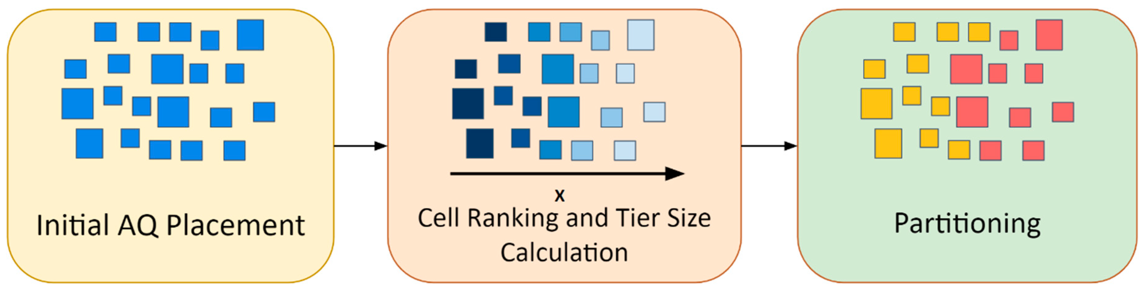
This section describes the details of the AQ partitioner, which divides the netlist into N equal parts. The AQ algorithm works by assigning each standard cell in the gate-level netlist into one specific tier out of the overall N tiers. The principal steps of the AQ partitioning system are outlined in
Figure 5. With the help of a placement algorithm, placed cells’ physical locations could be used as a discriminative metric for tier assignment.
As shown in
Figure 5, the tier assignment starts with performing an initial AQ placement on the given netlist. This 2D placement finds the location (x, y) of each cell to minimize the total wire length of the placed netlist. In its standard implementation, the initial step of AQ is followed by iterative partitioning, placement, and legalization [
32]. However, in this work, this initial step is taken as a representation of the placed netlist since it can be performed fast and is efficient in terms of spreading the cells. In order to implement the initial AQ placement, a new temporary net is inserted between each pair of connected cells, creating the fully connected clique model of the netlist. The connection matrix of all cells and pins are then extracted using the weights of each connection within the clique model. The optimum location for each cell placement is then calculated by setting the derivative of the total quadratic wire length to zero.
As seen in
Figure 6, having performed the initial AQ, the placed cells are ranked based on their location on the
x-axis, with the cells on the left side of the placed netlist having higher ranks than the cells on the right side. This partitioning approach is inspired by the recursive partitioning step of the AQ placement algorithm. To partition the netlist, cells in the ranking queue are assigned a specific tier (starting at the lowest tier) until the tier’s area limitation is reached. At this point, the tier is changed to the next higher one.
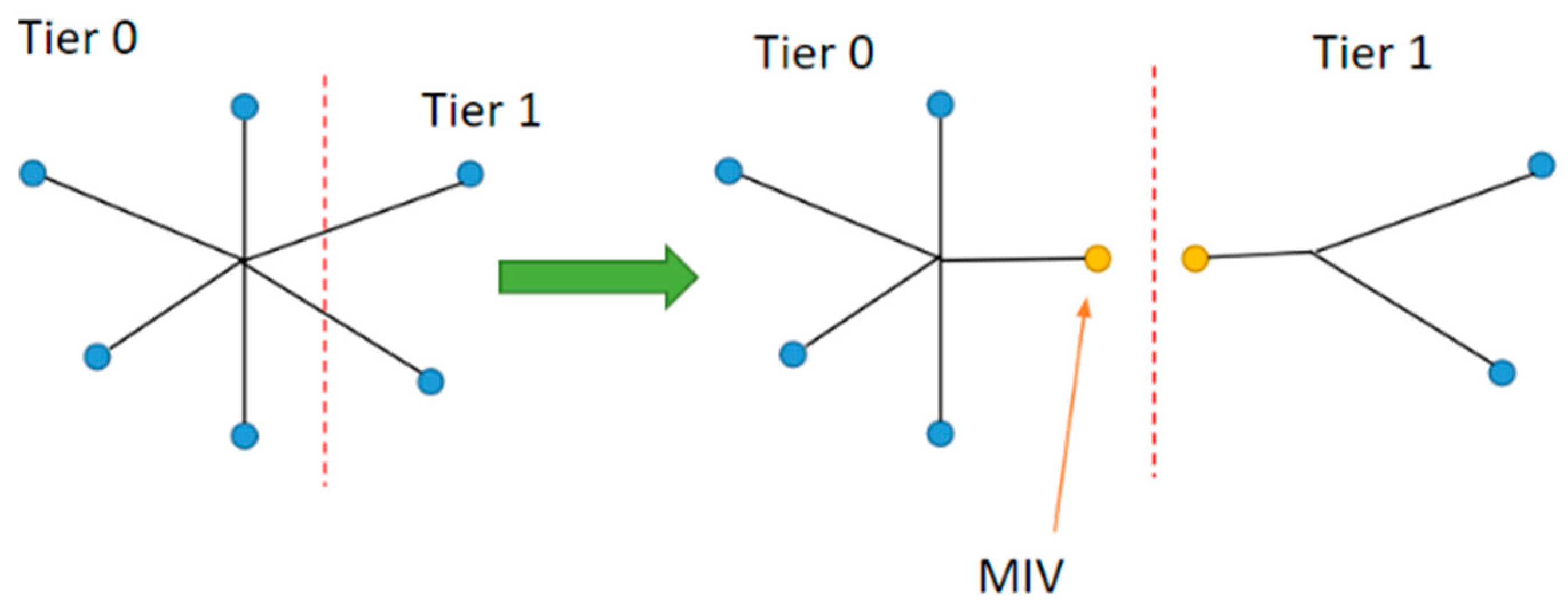
After the partitioning is performed and each cell is assigned a tier, there exist nets that have been spread across multiple tiers. In order to keep these connections intact, MIVs are inserted in the severed nets as an extra cell. The details of the MIV insertion process are described in detail in the next section.
2.3. MIV Insertion
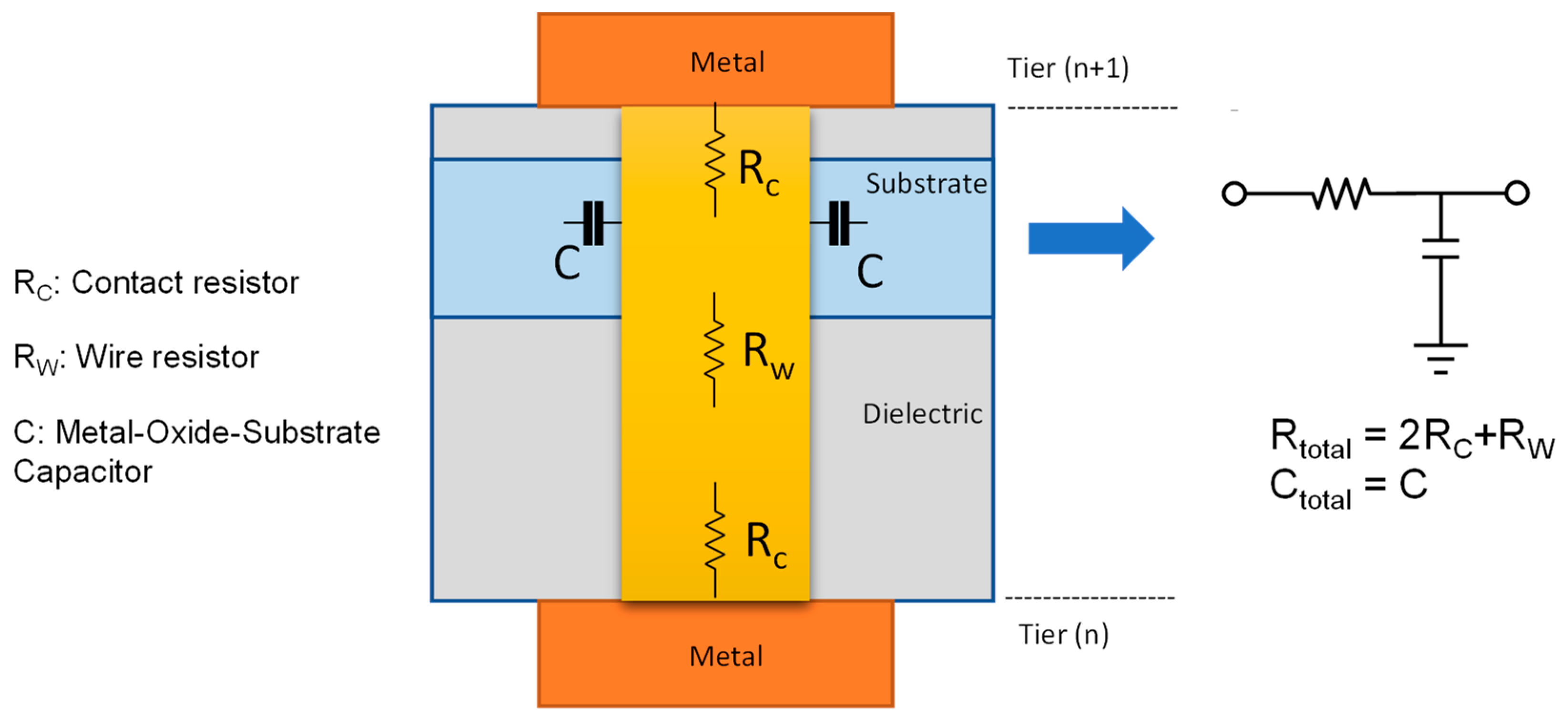
Vertical interconnects such as MIVs are used to carry the signal from one tier to the next. The general representation of an MIV is shown in
Figure 7, along with its equivalent circuit model. It consists of two contact resistances and a wire resistance in series with capacitor components with the substrate. Therefore, the MIV could be modelled as a resistor in series with a capacitance in parallel. The size of an MIV is negligible compared to the size of typical standard cells, so there is no density cap placed on the MIV placement. The overall resistance and capacitance of an MIV could be assumed to be 2 Ω and 0.1 fF, respectively, with an approximate diameter of 100 nm [
11]. The approximate size and parasitic capacitance of the MIVs are comparable to the antennae diode standard cell, which is already present in the technology library. Therefore, the antennae diode standard cell is used to simulate MIV cells. These cells are placed at the end of each of the nets, which are cut off by the tier-partitioning algorithm, as shown in
Figure 8. This insertion is also iteratively performed if the nets spread in more than two tiers, connecting the lowest tier to the highest tier that the net occupies.
Once the netlist is partitioned and MIVs are connected to the severed nets, all tiers are complete and can be saved as a netlist. Therefore, the outputs of the partitioning algorithms are N separate netlists, which are passed to physical design software for the P&R flow.
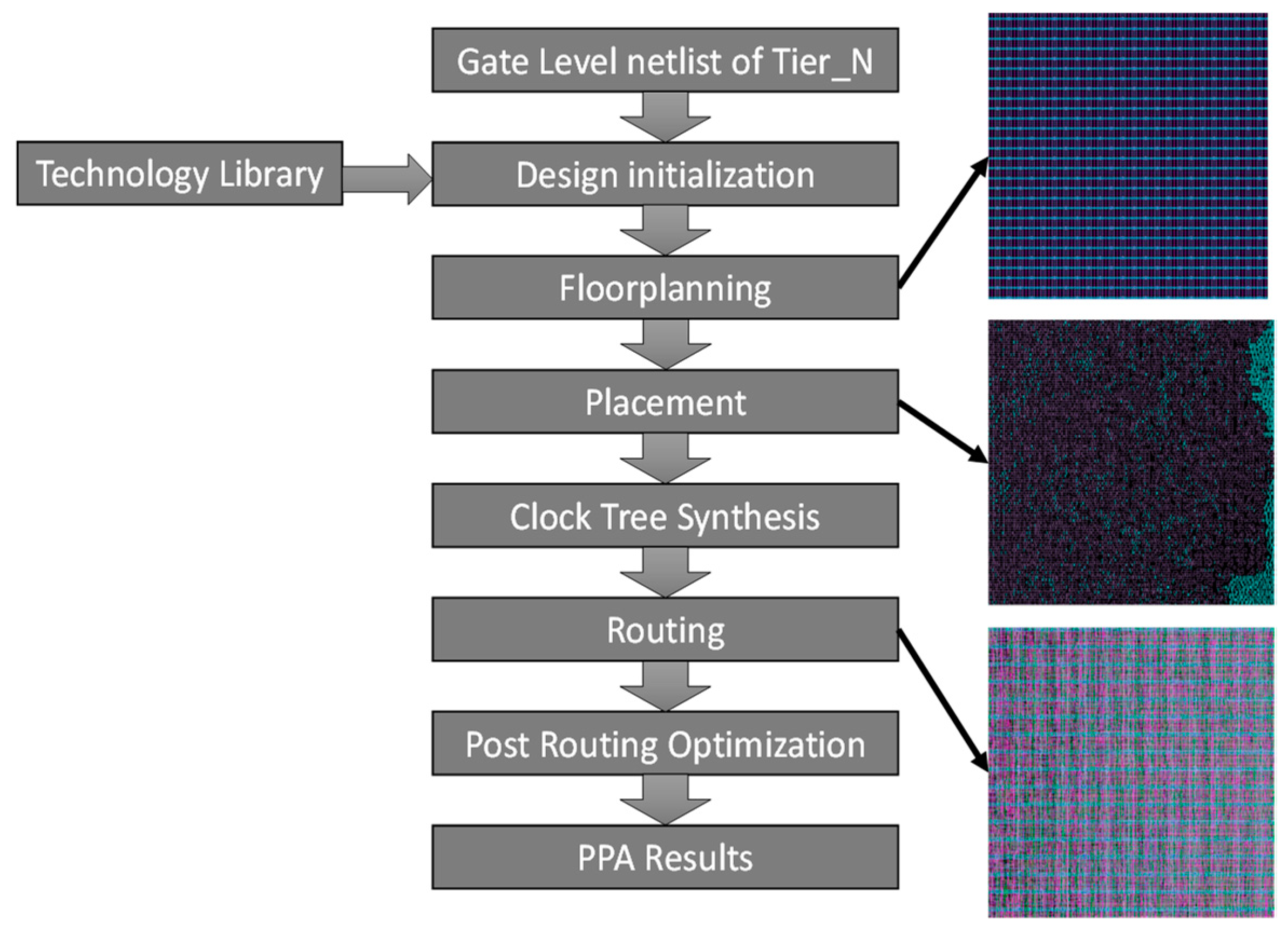
2.4. P&R Flow Using ICC2
The MIV insertion step is followed by the placement and routing implementation carried out with the ICC2 EDA tool. The detailed steps of this process are shown in
Figure 9. The first step of the flow is the design initialization, which sets up the design environment and loads the technology library into the system. A 32 nm standard cell library was used to implement the flow, which was obtained from Synopsys
®. The cell density of the different tiers of the 3D design are matched with that of the 2D design to aid in consistency and to achieve a fair result comparison. The design initialization is followed by the floor planning, which builds the PG grid and the core area. Each tier of the design consists of a total of nine metal layers to accommodate the interconnects.
This is followed by the placement of the cells and the clock tree synthesis to remove timing violations. Finally, the cells are connected in the routing step, followed by some postrouting optimizations. These optimizations are handled automatically by the P&R tool and include such things as fixing timing violations within tiers, making small changes in routing to optimize wire lengths, power optimizations, postroute buffer removal, etc. The power, performance, and area results are obtained for the individual tiers and added together to give the overall power dissipation of the entire 3D design.
3. Results
The entire design flow was executed on three different benchmark circuits: advanced encryption standard (AES), floating-point unit (FPU), and fast Fourier transform (FFT) circuits obtained from the
opencores.org website (accessed on 5 June 2020). These circuits differ in size and density and are used to demonstrate the applicability of 3D designs on different circuit types. The properties of the benchmark circuits are given in
Table 1.
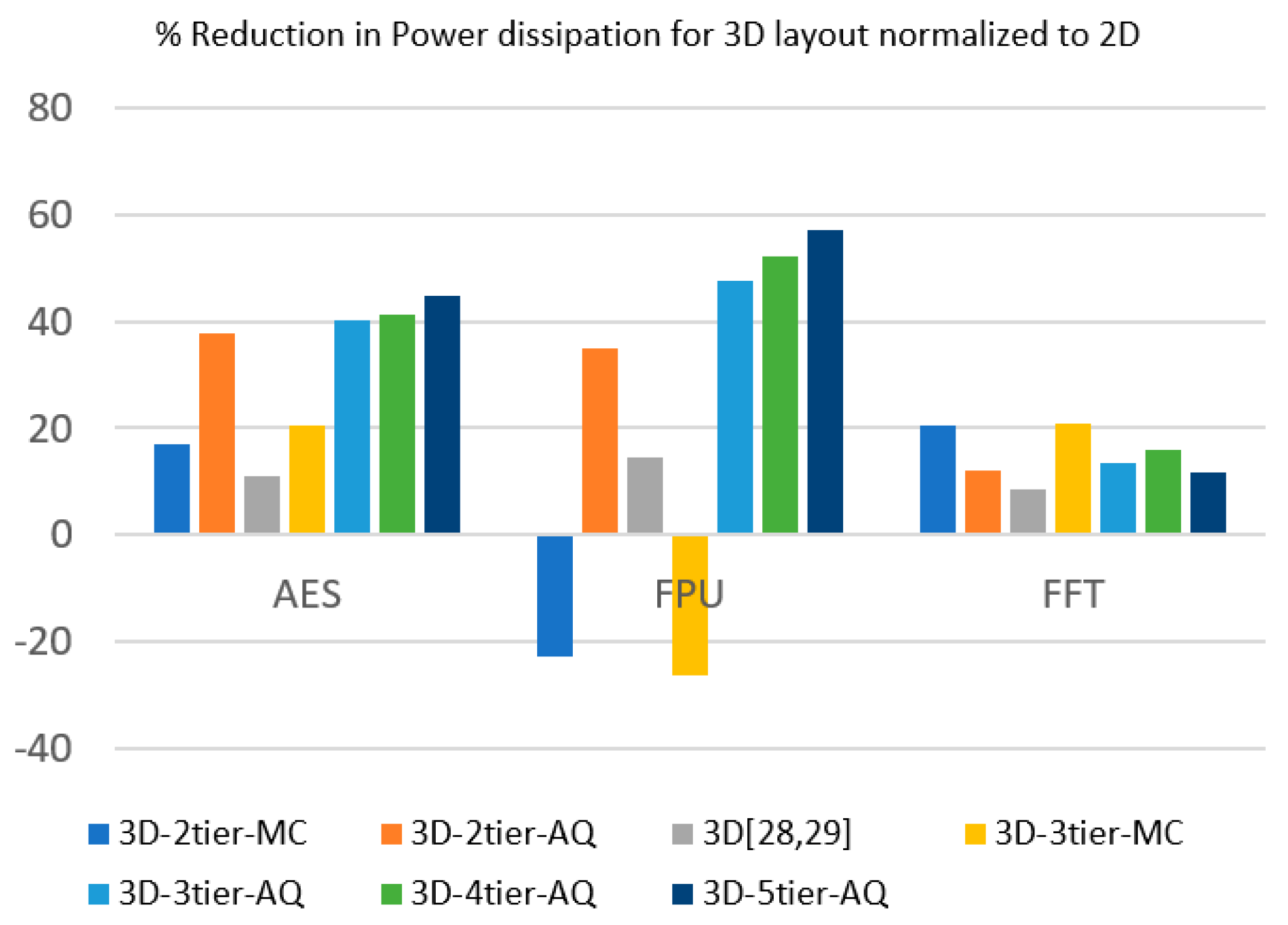
Power dissipation results have been studied for the 2D and 3D layouts for the benchmark circuits. Two-tier and three-tier models using the minimum-cut and analytical quadratic partitioning algorithms were developed and the reductions in power dissipation were compared with those from other similar studies [
28,
29]. Moreover, the four-tier and five-tier results were generated using the AQ partitioning for the benchmark circuits to show the trend in power dissipation as the total number of tiers in the 3D design were increased. The AQ algorithm was chosen for this analysis as it produces the best results.
Table 2 shows the power dissipation results and the percentage decrease in total power normalized to the 2D design for different 3D layouts and tier partitioning algorithms. The results are visualized in
Figure 10 and show that the AQ algorithm’s overall performance was better than that of the min-cut partitioning. The 3D results compared to the 2D counterparts were first analyzed. They show that the 3D implementation with the min-cut partitioning algorithm produced lower power dissipation for the AES and the FFT circuits while showing an increase in power dissipation for the FPU circuit. On the other hand, the results obtained with the AQ algorithm show a significant reduction in power for all the three benchmark circuits, with the AES circuit showing the most reduction in power dissipation for the two-tier models, while the FPU circuit showed the most power reduction for the higher-tier models. We also compared our results with those from other similar works [
28,
29], as shown in
Figure 10. The FFT 3D comparison results were obtained from [
28], where the 3TM metal layer structure was chosen as it produces the best results with no reduction in the metal dimensions, while the AES and the FPU comparison results were drawn from [
29], using the T-MI 3D design with the 45 nm node. Only two-tier 3D models were available in these studies. Our two-tier 3D layout developed using the min-cut partitioner produced better results than the related works [
28,
29] for the AES and FFT circuits, while our model comprising the AQ partitioner did significantly better in all three benchmark circuits. The most likely cause for the better power results of our implementation compared to [
28,
29] was better partitioning algorithms. However, the exact technology libraries and layout configurations of [
28,
29] differ from our implementation. As a result, the comparison between the different methods applied in this work alone are more valid compared to those between our implementation and other related studies [
28,
29].
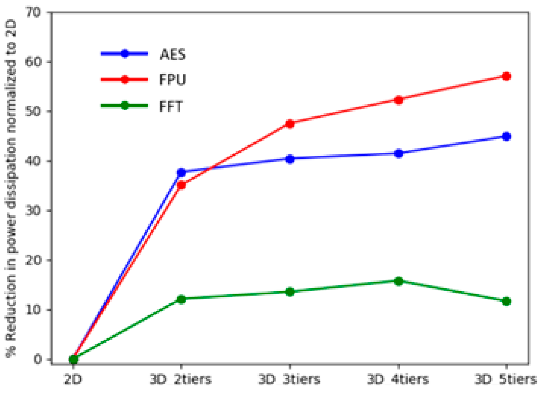
We next analyzed the reduction in power dissipation obtained by increasing the number of tiers of the 3D design using the AQ partitioner, as shown in
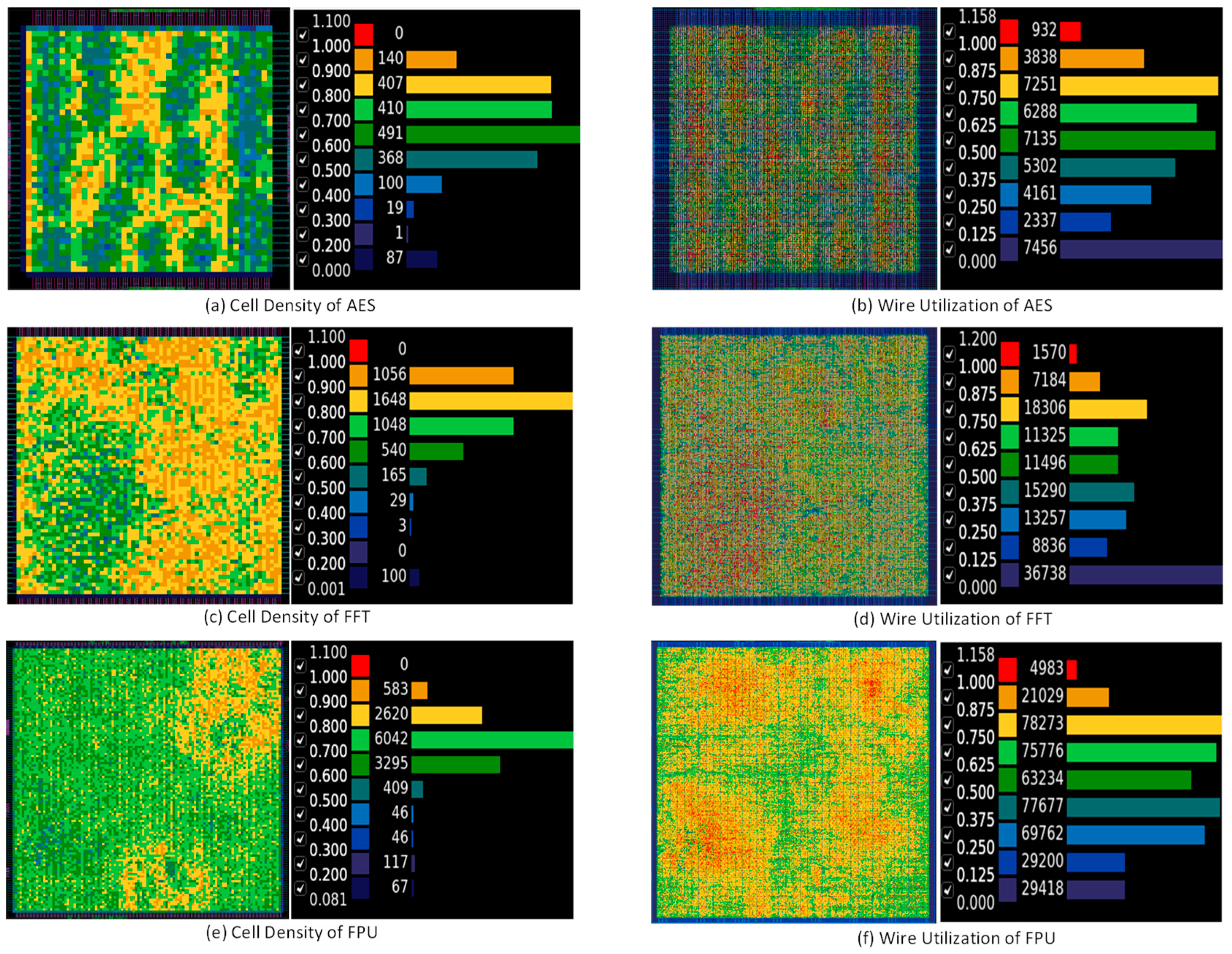
Figure 11. The results show a sharp decrease in power dissipation as we moved from the 2D layout to the two-tier 3D model, with smaller incremental decreases as we moved to higher tiers. The advantage of the 3D design in terms of reducing power dissipation is more prominent for circuits that are more wire dominant in nature. This makes the shift from 2D to 3D layouts more applicable for wire-intensive circuits than those that are more cell dominant. To analyze this fact further, the cell density and wire utilization plots for the three benchmark circuits were generated and are shown in
Figure 12. The cell density plots show the concentration of cells to be the highest in the FFT circuit, with those of AES and FPU being considerably lower. On the other hand, the wire utilization plots show the AES and the FPU circuits to have a more concentrated wire density than the FFT. This shows the FFT circuit to be much more cell dominant than the AES and the FPU, which are more wire dominant. Hence, the AES and FPU circuits are more suited for a 3D layout compared to the FFT circuit.
Moreover, the FFT circuit has a large clump of wires localized in the lower-left corner, making it more unsuitable for 3D implementation. These trends are confirmed by the 3D results that show the AES and the FPU’s overall 3D performance to be much better than the FFT circuit. The FFT circuit also saturated faster and even experienced an increase in power dissipation as we expanded it to a five-tier design. In contrast, the other two circuits showed a steady increase up to this point.
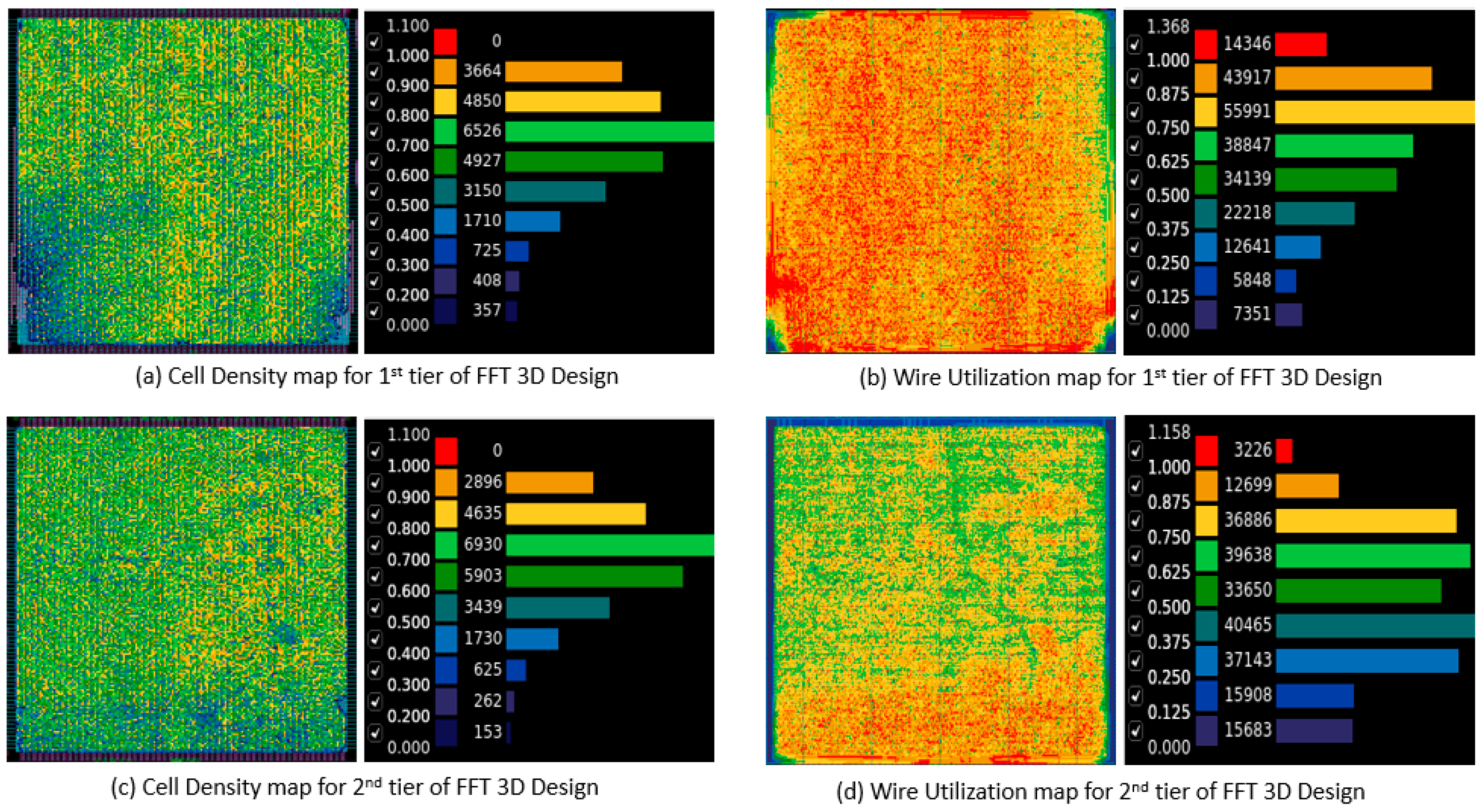
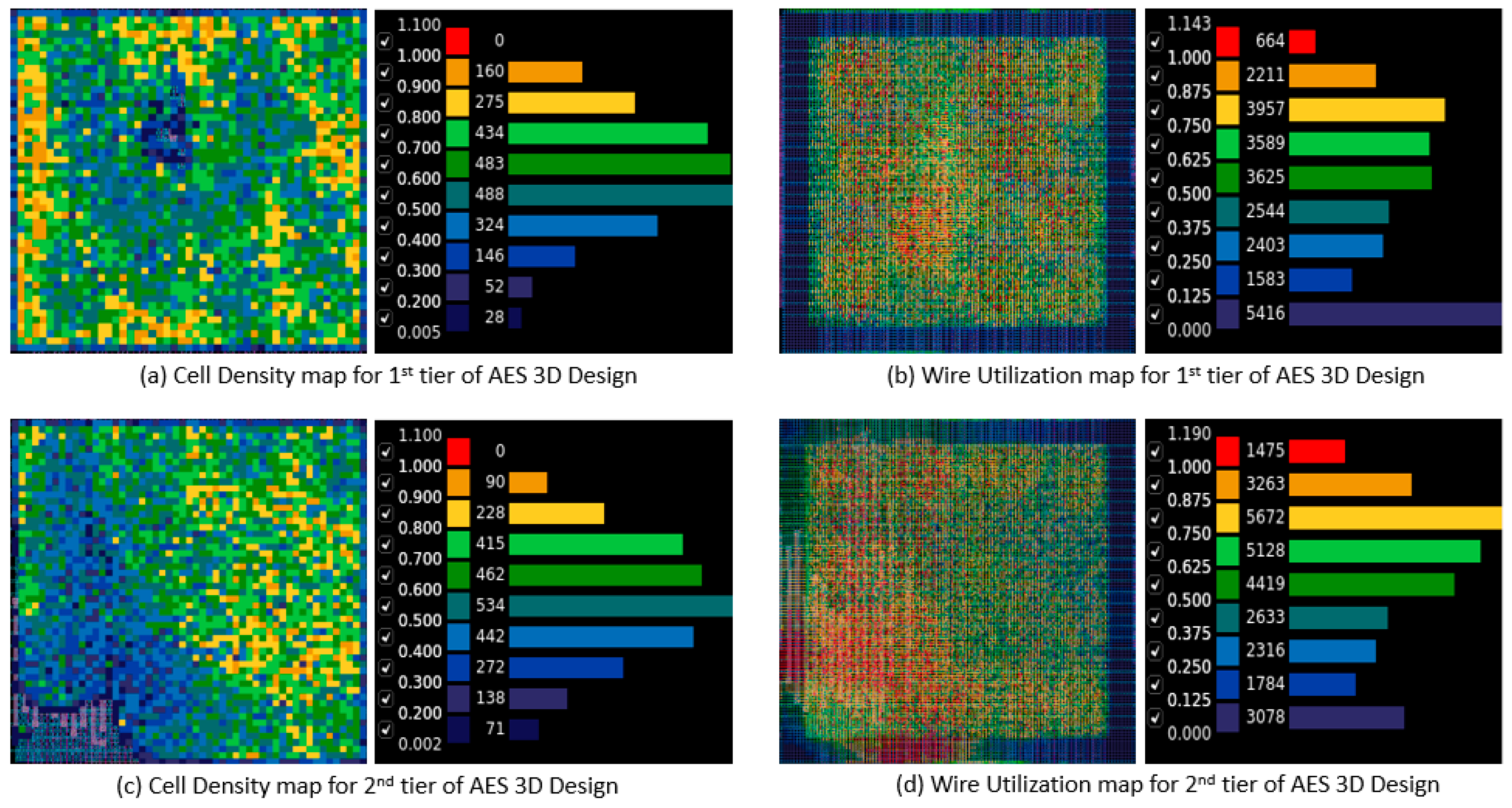
The cell density and wire utilization plots for the two-tier 3D design of the FFT and the AES benchmark circuits using the AQ partitioner are given in
Figure 13 and
Figure 14, respectively. The FPU benchmark circuit showed a similar trend, so the FFT and AES circuits are shown as examples. The plot shows even splitting of the cells among the two tiers. The plots show greater routing congestion for the FFT circuit compared to the AES circuit. Of note, the first tier of the FFT circuit showed very large wire utilization compared to the 2D design. This is confirmed by the power dissipation results, which show better 3D results for the AES circuit compared to the FFT circuit. The AES circuit, on the other hand, shows better wire utilization plots with very low wire utilization for the first tier and only two small hot spots in the second tier as well. This bolsters our earlier conclusion that more wire-dominant circuits like the AES have better 3D performance compared to more cell-dominant circuits like the FFT. However, in cell-dominant circuits like the FFT, there is significant difference between the wire utilization of the two tiers. This suggests that a partitioner that can better predict routing congestion would perform better for cell-dominant circuits compared to our proposed partitioning algorithms that are placement-based.
The timing analysis data for the 2D and two-tier 3D designs of the AES benchmark circuit are shown in
Table 3. Four different corner configurations were considered in the design. They are fast-fast at 125 °C, fast-fast at −40 °C, slow-slow at 125 °C, and slow-slow at −40 °C. The critical path length, slack, and clock period for the different corners are given in
Table 3 along with the number of violating paths and the total negative slack for the 2D and two-tier 3D AES circuits. The timing violation statistics for the AES 2D and two-tier 3D designs are shown in
Table 4. Both the 2D and 3D designs showed negligible violating nets compared to the total number of nets. The data shows similar timing performance for the 2D and the 3D circuits, so both the 2D and the two-tier 3D designs could be realized at a similar frequency.
However, our flow could only perform timing analysis on the nets that were confined to a single tier in the case of the 3D design and did not consider nets that travel between tiers. But a small portion of the overall nets travel in between tiers (less than 20% for the benchmark circuits), so the timing analysis of the 3D design could be considered as an approximation to the real results.
4. Discussion
Several further modifications could be made to increase the accuracy of the 3D model. These include implementing P&R of all the tiers together in the EDA tool instead of doing them separately. This would result in more accurate timing analysis and clock tree synthesis of the circuits. Another improvement to our current method could be achieved by implementing more detailed MIV modeling. In addition, different MIV models could be applied, and the results compared to investigate the effect of different types of MIVs on the performance of 3D ICs. Furthermore, the P&R flow could be modified to make sure that the connecting MIV cells in different tiers line up in the exact same physical locations in each tier to achieve more accurate results. The alignment of MIVs would ensure that cells on the partitioning border that were previously adjacent remain in close vicinity after tier partitioning, alleviating the problem of long routes between such cells. Moreover, the relationship between the MIV parasitic and the fan-in and fan-out of the logic gates should be analyzed in detail. These improvements and modifications are left as further work.
The time period of the 2D design and the individual tiers of the 3D design are set to be equal and only a small fraction of the nets go through the MIVs (about 18% for the two-tier AES design), so the 2D and the 3D designs are approximately iso performance. The implemented flow ensures that there are no timing violations among the nets that travel within tiers, but the flow does not have any mechanism to ensure that there are no timing violations in the fraction of the nets that travel in between tiers, and this accounts for a limitation in the study. However, the partitioner puts nets that are closely connected together in the same tier, so there are limited chances of timing violations being present in the inter-tier nets, and we leave the modification of the flow to include timing analysis for the inter-tier nets as future work.
The AQ partitioning runtime on the three benchmark circuits took less than 5 min each on a computer running on a standard Intel core i7 processor with 128GB of RAM. This shows that the AQ partitioning algorithm scales well and could be implemented easily on large industrial circuits as well.
5. Conclusions
The continuing trend in the reduction of the size of ICs is causing significant problems in the interconnect parasitic capacitance and resistance, which could be alleviated by moving to the 3D layout architecture. A complete design flow for the physical design of 3D ICs has been constructed in this study, which involves synthesizing the gate-level netlist from the RTL netlist, followed by tier partitioning and finally implementing the P&R flow.
The complete flow has been implemented on three benchmark circuits, which show significant reduction in the power dissipation of the 3D design compared to the 2D counterparts. Two different partitioning algorithms were implemented to assign the standard cells into different tiers. The AQ partitioning algorithm performed better on average compared to the min-cut algorithm on the three benchmark circuits that were used in the study.
The two-tier 3D flow power reduction compared to the 2D designs for the AES, FPU, and FFT benchmark circuits were 37.69%, 35.06%, and 12.15%, respectively, using the AQ partitioning algorithm. The power reduction steadily increased as the number of tiers for the 3D design was incremented. The steady decrease in the power dissipation was the most prominent for the FPU circuit and the least pronounced in the FFT circuit. Detailed analysis about the power reduction for the 3D architecture revealed that wire-dominant circuits like the AES are more applicable for 3D implementation than cell-dominant circuits like the FFT. The cell density and wire utilization heatmaps for the two-tier 3D designs for the FFT and the AES circuits using the AQ partitioner show that the cells are evenly distributed among the tiers for both the AES and the FFT circuits, whereas the wire utilization plot for the FFT circuit shows more hot spots compared to the AES circuit. This observation is supported by the power dissipation results, which show better 3D performance for the AES circuit compared to the FFT circuit.
Finally, the timing analysis and violation data for the 2D and two-tier 3D designs show comparable timing performance between the 2D and 3D designs, which ensures the designs are iso performance. Of note, the 3D flow implemented in this work could only perform timing analysis for the nets that were restricted within a single tier of the 3D design, but only a small fraction of the nets travel in between the tiers so the reported timing data are very close to the real values.


