Abstract
The impact of process variations on circuit performance has become more critical with the technological scaling, and the increasing level of integration of integrated circuits. The degradation of the performance of the circuit means economic losses. In this paper, we propose an efficient statistical gate-sizing methodology for improving circuit speed in the presence of independent intra-die process variations. A path selection method, a heuristic, two coarse selection metrics, and one fine selection metric are part of the new proposed methodology. The fine metric includes essential concepts like the derivative of the standard deviation of delay, a path segment analysis, the criticality, the slack-time, and area. The proposed new methodology is applied to ISCAS Benchmark circuits. The average percentage of optimization in the delay is 12%, the average percentage of optimization in the delay standard deviation is 27.8%, the average percentage in the area increase is less than 5%, and computing time is up to ten times less than using analytical methods like Lagrange Multipliers.
1. Introduction
The continuous technological scaling and the increase in the level of integration of the nanometer circuits have made the process variations a main concern in the design of integrated circuits [1,2]. Intra-die process variations, which can be spatially independent or correlated, are increasing in new technologies [2]. Random Dopant Fluctuations (RDF), body and gate line edge roughness, work-function and stress channel are, among others, the main causes of intra-die local variations in advanced technology nodes [3,4,5,6]. Process variations impact the performance parameter of the circuits [1,7,8,9,10,11,12,13,14]. Process variations have an impact on the delay, power, noise, ageing, soft errors, and leakage, among other performance parameters. Degraded circuit performance due to process variations reduces chip revenue [7].
Gate-sizing optimization techniques have been widely used to improve the performance of circuits. This optimization method can be done using analytical methods such Lagrange multipliers as in [15,16,17,18,19,20,21], or using heuristics and metrics as in [19,22,23,24,25,26,27,28,29,30,31]. Gate-sizing optimization techniques based in heuristics and metrics consume less computing time than analytical methods as Lagrange multipliers or Geometric Programming. In heuristic and metric optimization methods, the gate selection metric and the optimization methodology define the results of the optimization process. In [22], the objective of the methodology is to minimize the leakage of the circuit. Two metrics are used, the first metric based on the Yield Slack () identifies the gates with more timing resources, and the other metric () computes the timing yield and the leakage caused by changing the of the gate i. The gates with the highest metric scores are selected to resize. This methodology is quite accurate but computationally expensive. In [24], the objective is to maximize a profit function. One heuristic and two metrics are used. The first metric is based on the slack and preselects a set of critical gates, and the second selection metric () is used to measure the change in delay in the p-percentile after resizing the gate i. The gates with the highest metric scores are resized. This methodology is accurate, complex, and computationally expensive. In [25], the objective is to minimize the delay () of the circuit. Twenty percent of paths with the highest are selected, then, a recursive formula is used to increase and decrease the size of the gates until the delay converges to an acceptable value. In this case, the resizing metrics need more elements to select the gates that benefit the optimization of delay with the care of the area. In [27], the objective is to minimize . A heuristic, metric, and a cost function are used. The critical paths are selected using metrics based on statistical slack. The cost function () is used to optimize and of the critical gates. The cost function uses a factor, which provides more emphasis on the optimization of the standard deviation of the delay. This methodology considers the fan-in and fan-out of the gate i. This work provides good results in the percentage optimization of the delay standard deviation , but the delay and area are not the main concern. In [29], one heuristic and two metrics are used. The objective is to optimize the timing yield of the circuit. The first metric is based on the concept of criticality and is used to select the most critical gates to reduce the number of gates to analyze by the second metric. The second metric is computationally more expensive as it is based on the effective yield gradient (). The fan-in and fan-out cone of the analyzed gate i is considered. This metric and methodology is accurate but with cost in computing time. In [31], a heuristic and a metric are used to optimize the timing yield of the circuit. The metric is the adjacent criticality, which takes into account the criticality of the gate i and the criticality of the fan-out gates. This method is accurate but with cost in computing time.
This paper proposes a new methodology that includes a critical path selection method, a heuristic, two coarse selection metrics to preselect critical gates, and a fine metric to select the final set of gates to resize. The fine metric includes important concepts such as the derivative of the standard deviation of delay, the criticality, the slack time, and the area of the analyzed gate. The metric also includes the concept of the segment and the variations in the input transition time. The methodology is applied to ISCAS benchmark circuits, and it offers more benefit in delay reduction at lower area cost and computing time. This work focuses on independent intra-die process variations in the transistor threshold voltage (Vth) [13,32,33,34,35]. Even more, the extension of the results to consider other types of independent process variations is straightforward.
The organization of the rest of the paper is as follows. Section 2 presents the optimization methodology. Section 3 presents coarse strategies for pruning candidate gates. Section 4 presents the proposed accurate metric, named fine metric, to select the best candidate gates to improve circuit performance. Section 5 presents the heuristic sizing methodology. Section 6 presents simulation results on ISCAS benchmark circuits and a comparison with previous works. Finally, Section 7 presents the conclusions of this work.
2. Optimization Methodology
Figure 1 shows a flux diagram of our proposal oriented to optimize circuit yield based on a statistical framework. The first step is to read the circuit information. The second step is to obtain a set of critical paths using Deterministic Static Timing Analysis (DSTA) based on corner analysis. Then, the obtained set is pruned using Statistical Static Timing Analysis (SSTA). Next, candidate gates in the critical paths are selected using coarse strategies with a low computational cost. The first coarse strategy is based on a simple metric, and the second on the concept of gate criticality. Then, the fine selection metric is used to prune the set of candidate gates to be sized-up. It must be noted that the more expensive but accurate fine selection metric evaluates a smaller set of gates that were reduced by the low-cost coarse pruning strategies. A sizing heuristic is applied to a subset of the ranked candidate gates obtained after the fine metric selection. Then, circuit information is updated. If the area of the optimized circuit () is smaller than the area constraint () or the derivative of the mean delay is negative (), or the derivative of delay standard deviation is negative () the process continues; otherwise, the results are the optimized circuit. The main constraint in our optimization methodology is the area constraint (). The other two constraints are used for not sizing-up the gates of the circuit when the benefit is limited or even there is no benefit. DSTA and SSTA are applied to the optimized circuit to obtain the final timing information.
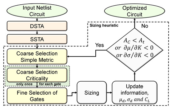
Figure 1.
Flow diagram of the proposed circuit performance optimization methodology.
3. Coarse Strategies for Pruning Candidate Gates
Two low-cost strategies are used for pruning candidate gates.
3.1. Coarse Selection Using a Simple Metric
The first coarse metric for pruning candidate gates is based on the nominal gate delay. The use of this coarse metric avoids making statistical evaluations saving computing time. Using the alpha-power law model [36], the nominal delay of a logic inverter can be expressed as
where is the load capacitance, is the power supply, L is the transistor channel length, is the gate oxide thickness, is the charge mobility in the transistor channel, is the dielectric constant, is the transistor voltage threshold, and is a constant that depends on the technology. where is the transistor channel width of a minimum-sized inverter and K is a scaling factor of the transistor size. Making the derivative of delay (d) in Equation (1) with respect to K gives the delay sensitivity of the inverter delay to small changes in the inverter size . For a given technology, the following expression for the delay sensitivity can be obtained:
In the previous expression, it can be observed that the impact of a small change of K on the nominal inverter delay depends only on and the inverter size K. Thus, Equation (2) can be used as an initial coarse metric for pruning the set of candidate gates. We want to highlight that only those logic gates having small values of delay sensitivities are discarded.
3.2. Coarse Selection Using the Gate Criticality
The gate criticality () is the number of times that a critical path crosses through a gate [17,31,37]. If the gate has a high criticality, it means that a significant number of critical paths share this gate. The gate criticality is usually used in metrics to select the best candidate gates [17,31,37], and we use it in the same way as shown later on. In addition, this work proposes to use the gate criticality for coarsely pruning candidates gates. Those gates having a low value of gate criticality are removed from the set of candidate gates.
4. Fine Selection Metric of Candidate Gates
4.1. Metric Fundamentals
The proposed fine metric is based on the evaluation of a path segment and modelling the input transition time as a normal distribution.
4.1.1. Path Segment Evaluation
For simplicity, a 5-inverter chain with different values of load capacitances (see Figure 2) is used to analyze the path segment behavior. The analyzed circuit allows for analyzing the relative impact on the standard delay of each gate when one gate is sized-up. A path segment of a logic path is defined as that composed by: (a) the gate to size-up, (b) the preceding gate, and c) the driven gate by the sized-up gate. For instance, the path segment when the gate is sized-up (See Figure 2) is composed by the gates , , and .
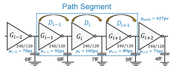
Figure 2.
Logic path composed of 5-inverters.
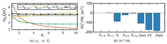
Figure 3a shows the behavior of the delay standard deviation of each gate in the 5-inverter chain as gate is sized-up. In addition, Figure 3b shows the relative impact on the delay variance of each gate as gate is sized-up by an amount . Figure 3a,b was obtained with SPICE. The following occurs when gate is sized-up:
- -
- The gate delay standard deviation of gate reduces because as indicated [38].
- -
- At the same time, the output driving current () of gate increases leading to faster output transitions and small output variations [39,40]. Consequently, the delay standard deviation of the gate decreases.
- -
- The load capacitance of the preceding gate increases, and as a consequence, the delay variance of the gate increases.
In addition, sizing-up inverter does not cause significant changes in the delay standard deviation of gates and . Similar behavior has been found for other gate sizes and loading conditions [29,31].
The previous behavior is consistent with Figure 3b showing the relative impact on the delay variance of each gate as gate is sized-up by an amount . In Figure 3b, it can also be observed that the sum of the changes of delay variances of each gate in the path segment (Sum) is lower than the change in delay variance of the path segment (PS). The difference between Sum and PS is due to the impact of the input transition time as will be explained next.
4.1.2. Modelling the Input Transition Time as a Normal Distribution
The second important issue considered in the proposed fine metric is that the variations in the input transition time [39,40,41,42,43,44,45] are modelled with a normal distribution. As a first consequence, the delay distribution (D) of a gate depends on both the normal distribution due to the independent variations in the transistor threshold voltage at the gate and variations at its input transition time (). As a second consequence, a covariance appears between the delays of two consecutive gates (e.g., Cov(;)). The correlation for this delay covariance is almost one as the output transition time of a gate is the input transition time of the next gate [41,42,43].
4.2. Fine Metric Formulation
4.2.1. Derivation of the Basic Fine Metric
The SPICE simulations (See Figure 3b) clearly show that the change in the delay variance of the path segment (PS) tracks the change well in the delay variance of the entire logic path Path when a gate is sized-up. Next, the fine metric is obtained. Let us first express the gate delay variance and the variance of the output transition time in terms of delay sensitivities due to small changes in the of the transistors and the gate input transition time (),
where is the delay sensitivity of gate i due to variations of its , is the variation of the transistor threshold voltage at gate i due to the manufacturing process, is the delay sensitivity of gate i due to variations at its input transition time, and is the variation of the input transition time at gate i. is the sensitivity of the output transition time due to changes in the of gate i.
The term depends on the previous gates (). Then, using (3) and (4), the standard deviation of delay of the gate i can be expressed as
The covariance between two consecutive gates in terms of the delay sensitivities requires first obtaining the delay distributions of two consecutive gates. Let us first to obtain the delay distribution of the gate ,
and the delay distribution of the gate i is expressed in a similar way,
Since the variations in are independent intra-die process variations, the covariance the delay distributions in (6) and (7) is given by
The change in the delay variance of a logic path when a gate i is sized-up by a small increment can be obtained by making the derivative of the delay variance of a logic path with respect to :
The first term in the previous equation is zero as it does not depend on a change in . The second, third, and fourth terms are different from zero because they are impacted by the re-sizing of the central gate as explained before. The fifth and sixth terms deserve a particular analysis.
Analysis of the fifth term in Equation (9)
Let us first analyze the fifth term of Equation (9). The delay variance of the gate can be obtained using (5). The change in delay variance of gate when the gate i is sized-up by a small increment can be expressed by
The first term on the right side in Equation (10) is zero as does not depend on changes.
In the second term, does not depend on variations in , therefore the second term in Equation (10) is zero. In the third and fourth term in Equation (10), ,, and do change due to variations in , but the variation of the product of the squared sensitivities is small enough not to be consider. As a result of that, the fifth term of Equation (9) can be neglected.
Analysis of the sixth term in Equation (9)
Let us now analyze the sixth term in Equation (9). The sixth term is composed of four terms of covariance between any pair of consecutive gates. These terms are , , . and .
Using Equation (8), the term can be expressed by
The previous term can be neglected because , y does not depend on the variations in .
Using Equation (8), the term can be expressed by
The previous term can be neglected because , , and do not change due to variations in .
The terms and have a strong dependence on the sized-up gate, and, hence, they should not be neglected.
Based on the previous analysis, the change in the delay variance of a logic path when a gate i is sized-up can be approximated by the change in the delay variance of the path segment as follows:
4.2.2. Basic Fine Metric
The covariance between adjacent gate can be expressed in terms of the product of their standard deviation and correlation ( between adjacent gates [41,45]):
The proposed metric is based on Equation (13), substituting Equation (14) in Equation (13), making the operations in Equation (13), and after ordering the terms gives,
Equation (15) represents the variations in the path segment due to size changes at gate [45].
4.2.3. Including Area, Gate Criticality, and Slack Time
The relative area cost of the gates is also considered. For instance, increasing the inverter size by a small increment has a different area cost than increasing a 3-Nand gate by the same amount . The gate area is computed by , where is the gate area for a minimum-sized symmetrical inverter allowed by the technology. In addition, gates with higher criticality are preferred. When resizing gates with high criticality, all the gates in the fan out cone of these gates improve their delay standard deviation at the same time, and the increase in area is only in the critical gates as in [17,31,37]. A gate belonging to a path with higher slack time is a better candidate gate [22,46]. The final fine selection metric including area cost, gate criticality, and slack time is as follows:
5. Sizing Heuristic
The sizing algorithm is composed of two parts. The first part evaluates the metrics, and the second part size-up those candidate gates selected by the metrics. A set of critical paths () is the input to the metrics. At the beginning of the process, two coarse selection metrics are applied. Then, the fine selection metric () is applied to the remaining gates. The gates are ranked according to their metric score, and one-quarter of the gates (n) selected by the fine metric is the final set of candidate gates for resizing (set(,)). In the second part of the algorithm, the gates are sized-up in proportion to its metric value (), where is the maximum size change that a gate can take at an iteration, and is the highest metric score. The obtained gate sizes with the optimization process are adjusted to comply the design rules of the technology. The maximum size of a gate is restricted to ten times its original size. The timing information and load capacitances are updated. Then, the process repeats until the restrictions are fulfilled.
The main target of our optimization process is to minimize the standard deviation of delay () with restriction in area. However, during the optimization process, both the standard deviation and the mean delay () reduce as the gates are sized-up. Figure 4a shows the change in the mean and standard deviation of the delay resizing gate in the logic path shown in Figure 2. A reduction in () as the gate is sized-up means that () is smaller than zero (See Figure 4b). Hence, in algorithm one, the optimization process ends according to the area restriction or if the derivative of () is greater than zero. It ensures that some of area, delay, or sigma variables do not deteriorate at the expense of the others.
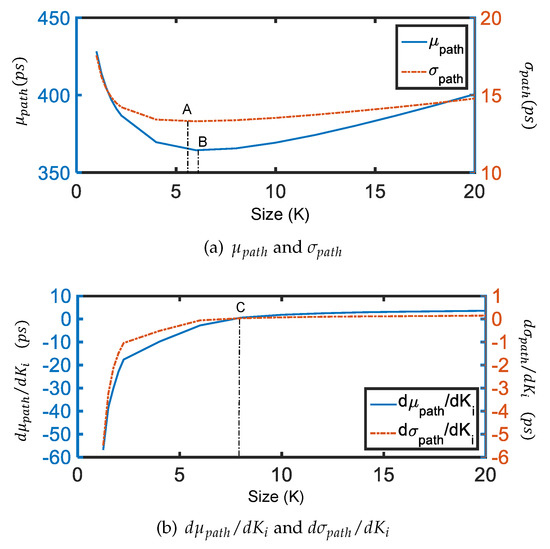
Figure 4.
(a) Mean and standard deviation of the delay of the logic path in Figure 2 when gate is sized-up; (b) derivative of the mean and standard deviation of the delay of the logic.
6. Simulation Results on the ISCAS Benchmark Circuits
An in-house tool that implemented the proposed flow in Figure 1 was developed. The algorithms have been written in C++ code. The effectiveness of our proposal has been validated on ISCAS 85 benchmark circuits implemented with a 65-nm technology. The layouts of the minimum-sized benchmark circuits have been obtained using the Mentor Graphics suite of synthesis and layout tools. Equation (15) is computed obtaining the delay sensitivities of each gate as a function of gate size, load capacitance, and input transition time. The gates delay sensitivities are obtained with SPICE, and MATLAB is used to adjust a polynomial at each sensitivity data. Polynomial expressions of the gate delay, output transition time, and delay sensitivities to changes in and are obtained. It must be noted that this process is just made once for the entire digital library of a given technology.
6.1. Fine Metric Validation
Figure 5 compares the optimization results of the analyzed logic path (See Figure 2) using the proposed fine metric against SPICE Monte Carlo simulations. Variations in of of its nominal value are used in the Monte Carlo analysis with 1000 Monte Carlo simulations to evaluate each run. Different areas are proposed for each gate of the analyzed logic path (See Figure 2). For each area combination of the gates in the path, the standard deviation of the path delay is measured. The obtained standard deviation of the path delay for the simulated area is plotted as a circle in Figure 5. On the other hand, the metric is applied repeatedly to the circuit in Figure 2, resizing the gate with the highest metric value in each iteration. For each iteration, the area and the standard deviation of path delay are measured. The path area and its respective standard deviation of the path delay are plotted on the blue line in Figure 5. The solid line corresponds to the optimized path with the lowest area cost. A close agreement between the results obtained with the fine metric and SPICE is observed.
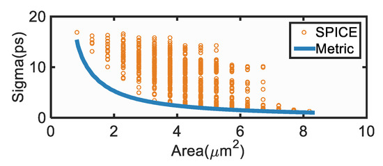
Figure 5.
Fine metric validation with SPICE using the logic path in Figure 2.
6.2. Benefit of the Low-Cost Pruning Strategies
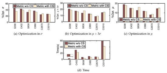
Figure 6.
Benefit in computing time using the coarse selection simple metrics (CS).
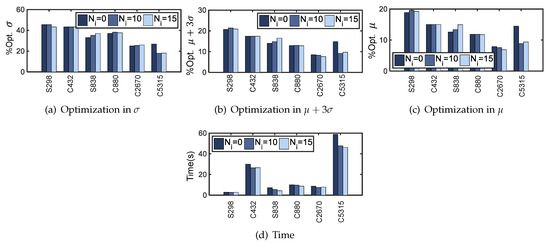
Figure 7.
Benefit in computing time using the coarse selection criticality (Crit).
Figure 6 shows the optimization results using the simple coarse metric and also only the fine metric selection (without the simple coarse metric). It can be observed that the percentage of optimization in , , and mean delay using the simple coarse metric follow the optimization results without the simple coarse metric. A small decrease in the optimization results appears in some cases, but this is not significant. Even more, a reduction in computing time can be observed when the simple coarse selection metric is used (see Figure 6d).
Figure 7 shows the optimization results using the criticality coarse metric and also only the fine metric selection (without the criticality coarse metric). It can be observed that the percentage of optimization in , , and , using the criticality coarse metric, follow the optimization results closely without the criticality coarse metric, but computing time is saved when the criticality coarse metric is used (see Figure 7d).
6.3. Optimization Results and Comparison
Table 1 shows an example step-by-step of Algorithm 1 for some ISCAS Benchmark circuits. First, the timing information of the circuits before the optimization is given. Table 1 shows the benefit in path pruning using DSTA and SSTA. It can also be observed that using the coarse metrics reduces the number of gates that will be analyzed by the fine metric. The reduction in the number of gates depends on the circuit topology. The results of the optimization process are illustrated at the right end of the Table 1. The circuit data information is updated after the optimization. Using DSTA and SSTA, the and of the longest critical path of the circuit is obtained.
| Algorithm 1: Algorithm sizing heuristic |
 |

Table 1.
Step by Step of process optimization for ISCAS 85 Benchmark Circuits (CMs = Coarse Metrics and FM = Fine Metric).
Table 2 shows the optimization results for 5% of area constraint. In addition, optimization results for the complete derivative of the delay variance of the logic path (DVP) and Lagrange method (L) are presented. The Lagrange methodology optimizes the delay standard deviation subject to the area restriction. The Lagrangian is solved using a gradient method. After optimization, the results of percentage optimization in delay standard deviation, delay, and area of our proposal follow those using the full derivative (DVP) of the logic path closely (see Table 2). In addition, our results approach those obtained with the Lagrange method. However, our proposal saves a significant amount of computing time.
Table 2.
Optimization results of our proposal, DVP and Lagrange.
6.4. Comparison with Previous Works
Our proposal was compared with the results from other authors. Papers from other authors present algorithms and implementations with specific strategies. Thus, this comparison is presented to indicate the benefits of our proposal in perspective with other works.
The results of our proposal also have been compared against the results in [27]. This work uses the delay variance as the objective function, and a cost metric function that maximizes the reduction in , to select gates. In [27] (See Table 3), the change in is positive. In our proposal, the change in is negative in all cases, which means that the delay always reduces after optimization. The reduction of the standard deviation of the delay in our proposal is slightly lower than in [27]. The increase in area is considerably smaller in our proposal. Finally, our proposal presents a lower cost in computing time.
Table 3.
Comparison between the results given in [27] and our proposal.
The results of our proposal also have been compared against the results in [25]. In work presented in [25], the objective of the methodology is to minimize . The methodology uses a heuristic and a metric. The average of the percentage of optimization in the mean delay in [25] is and with our proposal is . The average of the percentage of optimization in the variability () in [25] is and with our proposal is . The area increase in [25] is and with our proposal is only . It can be observed that our proposal presents good results trading-off the benefit in optimization and area penalization.
7. Conclusions
A statistical design methodology for circuit timing optimization has been proposed. A method to select critical paths is presented. The proposed methodology uses a heuristic, two low-cost coarse selection metrics, and a fine metric for selecting the best candidate gates to size-up. The use of coarse selection metrics allows a reduction in computing time. The basic fine metric allows for selecting the gates providing the higher benefit in the reduction of the delay standard deviation at the lowest area cost. Even more, the criticality and the slack-time are considered in the final fine metric. The use of path segment evaluation in the fine metric saves computing time. The proposed statistical design methodology has been validated on ISCAS benchmark circuits, the average of the percentage optimization in the delay standard deviation () is , the average of the percentage optimization in the delay () is , and the computing time is up to ten times less than Lagrange optimization methods. It should also be noted that the optimization results of the proposal are close to those obtained with Lagrange optimization method. The proposed statistical design sizing methodology is suitable for modern complex circuits.
Author Contributions
Investigation, Z.P.-R. and V.C.; Writing, review, and editing, Z.P.-R., E.T.-C. and V.C. All authors have read and agreed to the published version of the manuscript.
Funding
This work has been supported by The CONACYT (Mexico) through the PhD scholarship number 291025/68145.
Conflicts of Interest
The authors declare no conflict of interest.
References
- Nassif, S.R. Modelling and Analysis of Manufacturing Variations. In Proceedings of the IEEE 2001 Custom Integrated Circuits Conference, San Diego, CA, USA, 9 May 2001. [Google Scholar]
- Blaauw, D.; Chopra, K.; Srivastava, A.; Scheffer, L. Statistical Timing Analysis: From Basic Principles to State of the Art. IEEE Trans. Comput. Aided Des. Integr. Circuits Syst. 2008, 27, 589–607. [Google Scholar] [CrossRef]
- Dadgour, H.F.; Endo, K.; De, V.K.; Banerjee, K. Grain-Orientation Induced Work Function Variation in Nano Scale Metal-Gate Transistors—Part II: Implications for Process, Devices and Circuit Design. IEEE Trans. Electron Devices 2010, 57, 2515–2525. [Google Scholar] [CrossRef]
- Matsukawa, T.; Fukada, K.; Liu, Y.; Endo, K.; Tsukada, J.; Ishikawa, Y.; Yamauchi, H.; O’uchi, S.; Migita, S.; Mizubayashi, W.; et al. Fluctuation in Drain Induced Barrier Lowering (DIBL) for FinFets Caused by Granular Work Function Variation of Metal Gates. In Proceedings of the Technical Program-2014 International Symposium (VLSI-TSA), Hsinchu, Taiwan, 28–30 April 2014. [Google Scholar]
- Rasouli, S.H.; Endo, K.; Banerjee, K. Variability Analysis of FinFET-Based Devices and Circuits Considering Electrical Confinement and Width Quantization. In Proceedings of the 2009 IEEE/ACM International Conference on Computer-Aided Design-Digest of Technical, San Jose, CA, USA, 2–5 November 2009. [Google Scholar]
- Ojha, A.; Chauhan, Y.S.; Mohapatra, N.R. A Channel Stress-Profile-Based Compact Model for threshold Voltage Prediction of Uniaxial Strained HKMG nMOS Transistors. IEEE J. Electron Devices Soc. 2016, 4, 42–49. [Google Scholar] [CrossRef]
- Datta, A.; Bhunia, S.; Choi, J.H.; Mukhopadhyay, S.; Roy, K. Profit Aware Circuit Design Under Process Variations Considering Speed Binning. IEEE Trans. Very Large Scale Integr. (Vlsi) Syst. 2008, 16, 806–815. [Google Scholar] [CrossRef]
- Mahmoodi, H.; Mukhopadhyay, S.; Roy, K. Estimation of Delay Variations due to Random Dopant Fluctuactions in Nanoscale CMOS Circuit. IEEE J. Solid State Circuits 2005, 40, 1787–1796. [Google Scholar] [CrossRef]
- Kou, L.; Robinson, W.H. Impact of Process Variations on Reliability and Performance of 32nm 6T at Near Threshold Voltage. In Proceedings of the 2014 IEEE Computer Society Annual Symposium on VLSI, Tampa, FL, USA, 9–11 July 2014. [Google Scholar]
- Kansal, S.; Lanuzza, M.; Corsonello, P. Impact of Random Process Variations on different 65nm SRAM cell topologies. In Proceedings of the Third International Conference on Emerging Trends in Engineering and Technology, Goa, India, 19–21 November 2010. [Google Scholar]
- Arulvani, M.; Karthikeyan, S.S.; Neelima, N. Investigation of Process Variation on Register Files in 65nm Technology. In Proceedings of the International Conference on Emerging Trends in VLSI, Embedded System, Nano Electronics and Telecomunication System (ICEVENT), Tiruvannamalai, India, 7–9 January 2013. [Google Scholar]
- Abhishek, D.; Srekan, O.; Gokhan, M.; Joseph, Z.; Alok, C. Microarchitectures for Managing Chip Revenues Under Process Variations. IEEE Comput. Archit. Lett. 2008, 6, 29–32. [Google Scholar]
- Wang, X.; Cheng, B.; Brown, A.R.; Millar, C.; Asenov, A. Statistical Variability in 14nm node SOI FinFets and its Impact on Corresponding 6T-SRAM Cell Design. In Proceedings of the European Solid-State Device Research Conference (ESSDERC), Bordeaux, France, 17–21 September 2012. [Google Scholar]
- Alioto, M.; Consoli, E.; Palumbo, G. Variations in Nanometer CMOS Flip-Flops: Part I Impact of Process Variations on Timing. IEEE Trans. Circuits Syst. Regul. Pap. 2015, 62, 2035–2043. [Google Scholar] [CrossRef]
- Chen, C.; Chris, C.N.; Wong, D.F. Fast and Exact Simultaneous Gate and Wire Sizing by Lagarngian Relaxation. IEEE Trans. Comput. Adided Des. Integr. Circuits Syst. 1999, 18, 1014–1025. [Google Scholar] [CrossRef]
- Champac, V.; Reyes, A.N.; Gomez, A.F. Circuit Performance Optimization for Local Intra-Die Process Variations Using Gate Selection Metric. In Proceedings of the IFIP/IEEE International Conference on Very Large Scale Integration (VLSI-SoC), Daejeon, Korea, 5–7 October 2015. [Google Scholar]
- Raj, S.; Vrudhula, S.B.K.; Wang, J.A. Methodology to Improve Timing Yield in the Presence of Process Variations. In Proceedings of the 41st Design Automation Conference, San Diego, CA, USA, 7–11 July 2004. [Google Scholar]
- Davoodi, A.; Siravastava, A. Variability Driven Gate Sizing for Binning Yield Optimization. IEEE Trans. Very Large Scale Integr. (Vlsi) Syst. 2008, 16, 683–692. [Google Scholar] [CrossRef]
- Lu, Y.; Shang, L.; Zhou, H.; Zhu, H.; Yang, F.; Zeng, X. Statistical Reliability Analysis Under Process Variation and Aging Effects. In Proceedings of the 2009 46th ACM/IEEE Design Automation Conference, San Francisco, CA, USA, 26–31 July 2009. [Google Scholar]
- Choi, S.H.; Paul, B.C.; Roy, K. Novel Sizing Algorithm for Improvement under Process Variation in Nanometer Technology. In Proceedings of the 41st Design Automation Conference (DAC’04), San Diego, CA, USA, 7–11 July 2004. [Google Scholar]
- Sun, J.; Wang, J. Robust Gate Sizing by Uncertainty Second Order Cone. In Proceedings of the 11th International Symposium on Quality Electronic Design (ISQED), San Jose, CA, USA, 22–24 March 2010. [Google Scholar]
- Hwang, E.J.; Kim, W.; Kim, Y.H. Timing Yield Slack for Timing Yield-Constrained Optimization and its Appliation to Statistical Leakage Minimization. IEEE Trans. Very Large Scale Integr. (Vlsi) Syst. 2013, 12, 1783–1796. [Google Scholar] [CrossRef]
- Raji, M.; Ghavami, B. Soft Error Rate Reduction of Combinational Circuits Using Gate Sizing in the Presence of Process Variations. IEEE Trans. Very Large Scale Integr. (Vlsi) Syst. 2017, 25, 247–260. [Google Scholar] [CrossRef]
- Agarwal, A.; Chopra, K.; Blaauw, D.; Zolotov, V. Circuit Optimization using statistical timing analysis. In Proceedings of the 42nd Design Automation Conference 2005, Anaheim, CA, USA, 13–17 June 2005. [Google Scholar]
- Yelamarthi, K.; Chen, C.H. A timing optimization technique for Nanoscale CMOS circuits susceptible to process variations. In Proceedings of the IEEE International Instrumentation and Measurement Technology Conference, Binjiang, China, 10–12 May 2011. [Google Scholar]
- Sreemath, K.; Ramesh, S.R. Statistical Viability Analysis and Optimization Through Gate Sizing; Bhattacharya, S., Gandhi, T., Sharma, K., Dutta, P., Eds.; Advanced Computational and Communications Paradigms Lecture Notes in Electrical Engineering; Springer: Singapore, 2018. [Google Scholar]
- Neiroukh, O.; Song, X. Improving the Process Variation Tolerance of Digital Circuits Using Gate Sizing and Statistical Techniques. In Proceedings of the Design, Automation and Test in Europe Conference exhibition (DATE’05), Munich, Germany, 7–11 March 2005. [Google Scholar]
- Tsai, C.; Cheng, C.; Huang, N.; Wu, K. Analysis and Optimization of Variable-Latency Design in the Presence of Timing Variability. In Proceedings of the Design, Automation Test in Europe Conference Exhibition (DATE), Lausanne, Switzerland, 27–31 March 2017. [Google Scholar]
- Ramprasath, S.; Vasudevan, V. An Efficient Algorithm for Statistical Timing Yield Optimization. In Proceedings of the 2015 52nd ACM/EDAC/IEEE Design Automation Conference (DAC), San Francisco, CA, USA, 8–12 June 2015. [Google Scholar]
- Sinha, D.; Shenoy, N.V.; Zhou, H. Statistical gate sizing for timing yield optimization. In Proceedings of the ICCAD-2005 IEEE/ACM International Conference on Computer-Aided Design, San Jose, CA, USA, 6–10 November 2005. [Google Scholar]
- Ebrahimipour, S.M.; Ghavami, B.; Raji, M. Adjacent Criticality: A Simple However, Effective Metric for Statistical Timing Yield Optimization of Digital Integrated Circuits. IET Circuits Devices Syst. 2019, 13, 979–987. [Google Scholar] [CrossRef]
- Hassan, F.; Vanderbauwhede, W.; Rodriguez, F.S. Impact of Random Dopant Fluctuactions on Timing Characteristics of Flip-Flop. IEEE Trans. Very Large Scale Integr. (Vlsi) Syst. 2012, 20, 157–161. [Google Scholar] [CrossRef]
- Chung, S.S. The Variability Issues in Small Scale Trigate CMOS Devices: Random Dopant and Trap Induced Fluctuations. In Proceedings of the 20th IEEE International Symposium on the Physical and Failure Analysis of Integrated Circuits (IPFA), Suzhou, China, 15–19 July 2013. [Google Scholar]
- Zhang, K.; Chen, Y.; Dong, Y.; Xie, Z.; Zhao, Z.; Si, P.; Yu, T.; Dai, L.; Lv, W. Effect of Random Channel Dopant on Timing Variation for Nanometre CMOS Inverters. In Proceedings of the IEEE 2nd International Conference on Electronics Technology (ICET), Chengdu, China, 10–13 May 2019. [Google Scholar]
- Ye, Y.; Liu, F.; Chan, M.; Nassif, S.; Cao, Y. Statistical Modeling and Simulation of Threshold variations Under Random Dopant Fluctuactions and Line Edge Rougness. IEEE Trans. Very Large Scale Integr. (Vlsi) Syst. 2011, 19, 987–996. [Google Scholar] [CrossRef]
- Sakurai, T.; Newton, A.R. Alpha - Power Law Model and its Application to CMOS Inverter Delay and other Formulas. IEEE J. Solid State Circuits 1990, 25, 584–594. [Google Scholar] [CrossRef]
- Guthaus, M.R.; Venkateswarant, N.; Visweswariaht, C.; Zolotov, V. Gate Sizing Using Incremental Parameterized Statistical Timing Analysis. In Proceedings of the ICCAD-2015 IEEE/ACM International Conference on Computer-Aided Design, San Jose, CA, USA, 6–10 November 2005. [Google Scholar]
- Pelgrom, J.M.; Duinmaijer, C.J.; Welbers, P.G. Matching Properties of MOS Transistors. IEEE J. Solid State Circuits 1989, 24, 1433–1439. [Google Scholar] [CrossRef]
- Roy, S.; Pan, D.Z. Reliability Aware Gate Sizing Combating NBTI and oxide Breakdown. In Proceedings of the 2014 27th International Conference on VLSI Design and 2014 13th International Conference on Embedded Systems, Mumbai, India, 5–9 January 2014. [Google Scholar]
- Ozdal, M.M.; Burns, S.; Hu, J. Algorithms for Gate Sizing and Device Parameter Selection for High-Performance Design. IEEE Trans. Comput. Aided Des. Integr. Circuits Syst. 2012, 31, 1558–1571. [Google Scholar] [CrossRef]
- Shin, S.; Yu, W.; Jun, Y.; Kim, J.; Kong, B.; Lee, C. Slew Rate Controlled Output Driver Having Constant Transition Time Over Process, Voltage Temperature, and Output Load Variations. IEEE Trans. Circuits Syst. 2007, 54, 601–605. [Google Scholar] [CrossRef]
- Kouno, T.; Onodera, H. Consideration of Transition-Time Variability in Statistical Timing Analysis. In Proceedings of the IEEE International SoC Conference, Taipei, Taiwan, 24–27 September 2006. [Google Scholar]
- Chang, H.; Sapatnekar, S. Statistical Timing Analysis Under Spatial Correlations. IEEE Trans. Comput. Aided Des. Integr. Circuits Syst. 2005, 24, 1467–1482. [Google Scholar] [CrossRef]
- Livramento, V.; Guth, C.; Johann, M.O. Evaluating the Impact of Slew on Delay and Power of Neighbouring Gates in Discrete Gate Sizing. In Proceedings of the IEEE 3rd Latin American Symposium on Circuits and Systems (LASCAS), Playa del Carmen, Mexico, 29 February–2 March 2012. [Google Scholar]
- Perez, Z.; Villacorta, H.; Champac, V. An Accurate Novel Gate-Sizing Metric to Optimize Circuit Performance Under Local Intra-Die Process Variations. In Proceedings of the 2018 IFIP/IEEE International Conference on Very Large Scale Integration (VLSI-SoC), Verona, Italy, 8–10 October 2018. [Google Scholar]
- Hwang, E.J.; Kim, W.; Kim, Y.H. Timing Yield Slack for Timing Statistical Optimization. In Proceedings of the 2011 3rd Asia Symposium on Quality Electronic Design (ASQED), Kuala Lumpur, Malaysia, 19–20 July 2011. [Google Scholar]


© 2020 by the authors. Licensee MDPI, Basel, Switzerland. This article is an open access article distributed under the terms and conditions of the Creative Commons Attribution (CC BY) license (http://creativecommons.org/licenses/by/4.0/).