Article

Dependence of Irradiated High-Power Electromagnetic Waves on the Failure Threshold Time of Semiconductors Using a Closed Waveguide

1
Korea Institute of Radiological and Medical Sciences (KIRAMS), Seoul 01812, Korea
2
Electro-Medical Device Research Center, Korea Electrotechnology Research Institute, Ansan 15588, Korea
3
Center for THz-Driven Biomedical Systems, Department of Physics and Astronomy, College of Natural Sciences, Seoul National University, Seoul 08826, Korea
4
Center for Applied Electromagnetic Research, Advanced Institute of Convergence Technology, Suwon 16229, Korea
5
R&D Department, Seoul-Teracom, Inc., Suwon 16229, Korea
6
Young IN ACE, 1F, 60, Anyangcheondong-ro, Dongan-gu, Anyang-si 14042, Korea
7
Home Economics Education/Biosystems and Biomedical Sciences, Korea University, Seoul 02841, Korea
*
Author to whom correspondence should be addressed.
Electronics 2021, 10(16), 1884; https://doi.org/10.3390/electronics10161884
Submission received: 18 June 2021 / Revised: 3 August 2021 / Accepted: 3 August 2021 / Published: 6 August 2021

Abstract

:
The failure threshold time of semiconductors caused by the impact of irradiated high-power electromagnetic waves (HPEM) is experimentally studied. A SN7442 integrated circuit (IC) is placed in an emulator with a WR430 closed waveguide and is irradiated by HPEM generated from a magnetron oscillator. The state of the SN7442 component is observed by a light-emitting diode (LED) detector and the voltage measured in the SN7442 component. As the magnitude of the electric field in the HPEM is varied from 24 kV/m to 36 kV/m, the failure threshold time falls from 195 s to 17 s with dependence of the irradiated electric field (E) on the failure threshold time (T) from T~E−12 to a T~E−6.

1. Introduction

High-power electromagnetic waves (HPEM) reach a target, and a sequential process of penetration and propagation occurs from the target’s outer surface into its interior as the waves arrive at the electronics of the target. Modern electronic systems are principally composed of semiconductor devices, which are made primarily of silicon and gallium arsenide. These are of vital importance for the function of security systems, traffic systems and modern communication systems, and a malfunction induced by the irradiation effects of HPEM in one of these areas can cause casualties and economic disasters [1,2,3,4]. Therefore, the susceptibility of electronics to electromagnetic waves is of great interest. Theoretical predictions and experimental comparisons using a semiconductor diode have been done to inspect the dependence of the voltage pulse width on the destruction power density [5]. A failure mechanism due to a reduction on the resistance resulting from the formation of a thin conductive layer by a DC pulse is observed in a metal semiconductor field-effect transistor (MESFET) [6]. Using an open waveguide, the destructive effects of a semiconductor, in this case, transistor-transistor-logic (TTL) and a complementary metal-oxide semiconductor (CMOS) technology-based device, caused by the impact of an electromagnetic pulse (EMP) and ultra-wideband (UWB) frequency were investigated to measure the susceptibility of electronic devices to a transient electromagnetic field threat [7,8,9].
With the advent of the fourth industrial era, the frequency of use of digital wireless information devices is increasing, and the demand for a new system that can quickly process large amounts of information anywhere is increasing. For this reason, the demand for the use of high frequencies higher than the frequency bandwidth currently in use is gradually increasing. The increase in the use of information devices and the dependence on information devices for the information age are also increasing. It has been reported that information equipment may malfunction or be damaged due to the effects of transient electromagnetic waves from a high-power electromagnetic wave generator operating in the frequency range of the same band. High-power microwaves (HPM) are currently being researched and developed to generate gigawatt (GW) level electromagnetic waves in a short pulse (~100 ns), with the dominant operating frequency being 1–10 GHz, but other derived frequencies exceed 30 GHz. HPM devices developed in various countries such as the United States, Russia, China, and Japan as well as several countries in Europe can be viewed as being mainly studied for military purposes. However, as described above, intentionally generated electromagnetic waves can cause serious damage to information equipment [10,11,12,13,14,15,16,17,18]. HPEM emulators used to measure the level at which private information devices and systems are upset by high-power transient electromagnetic waves through simulations are more effective than a gigawatt-level electromagnetic wave generator. For these basic studies, it is crucial to provide basic data for the development of an HPEM emulator.
In this paper, the dependence of irradiated HPEM on the failure threshold time is experimentally studied using a SN7442 IC in a WR430 closed waveguide emulator when the magnitude of the irradiated electric field generated from a magnetron oscillator is varied from 24 kV/m to 36 kV/m (equivalent to the range from 1.9 kW/cm2 to 4.27 kW/cm2).

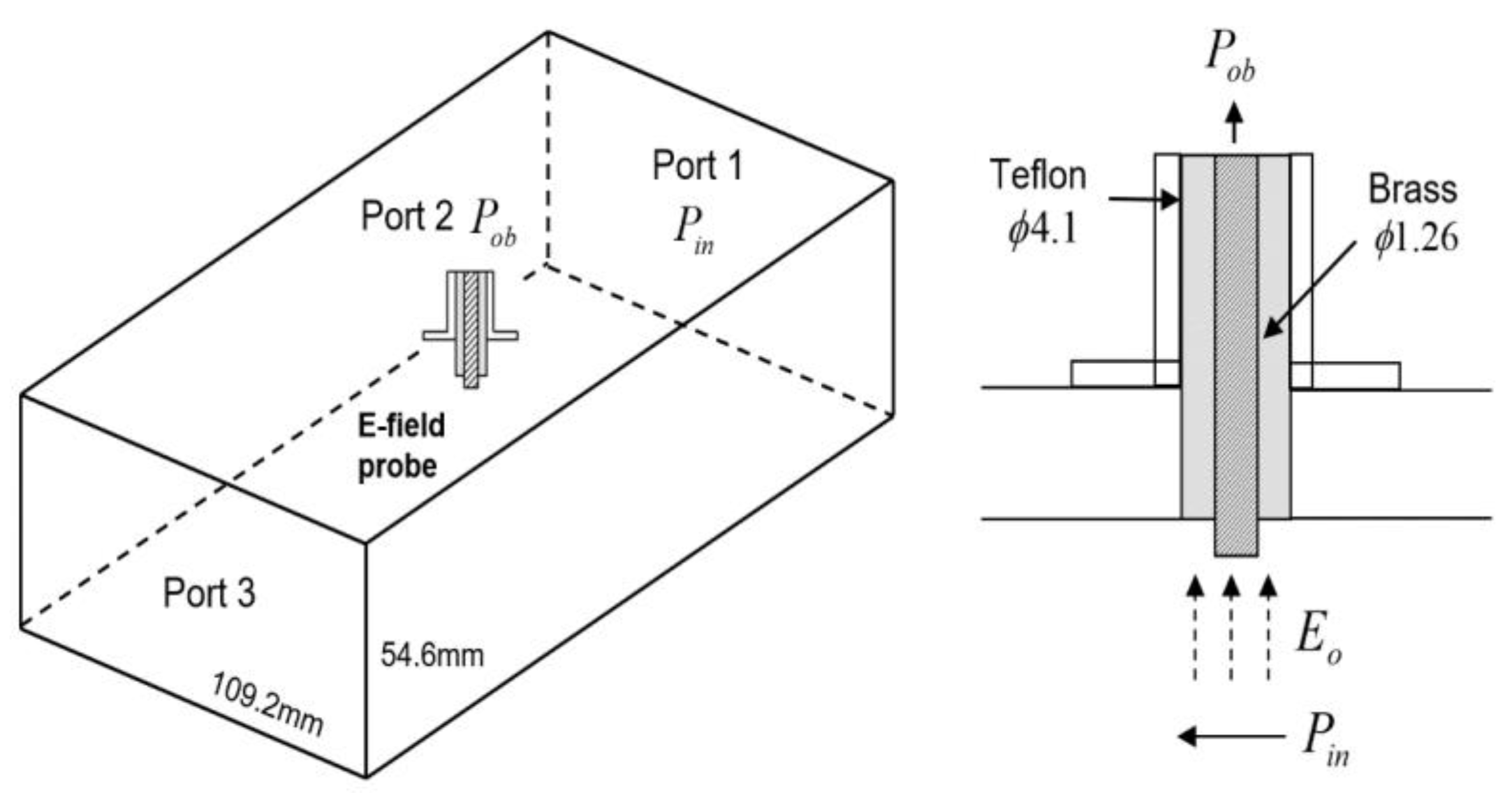
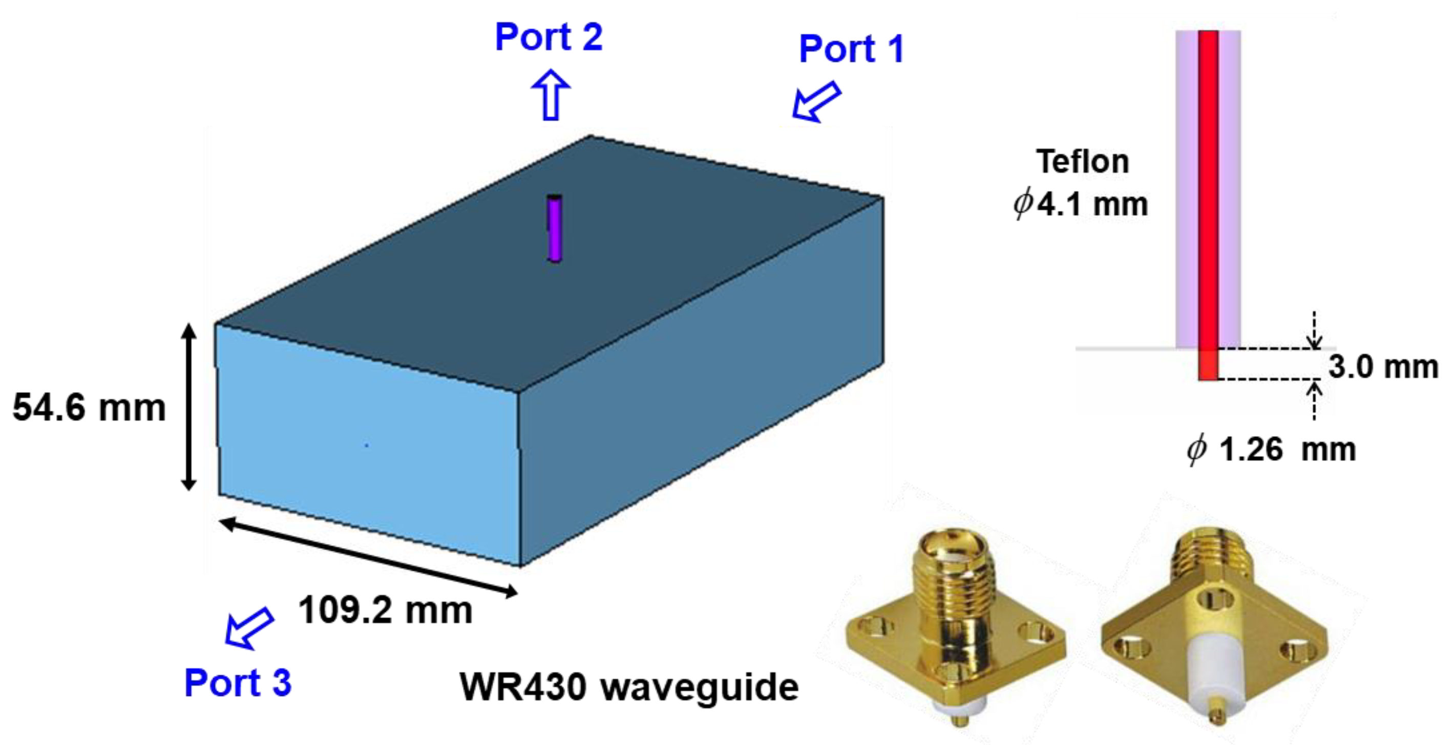
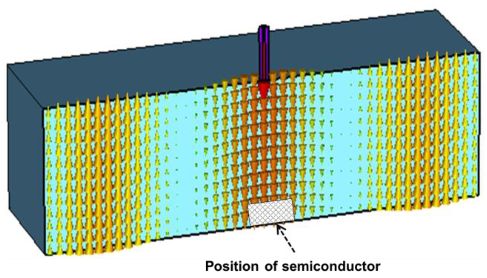
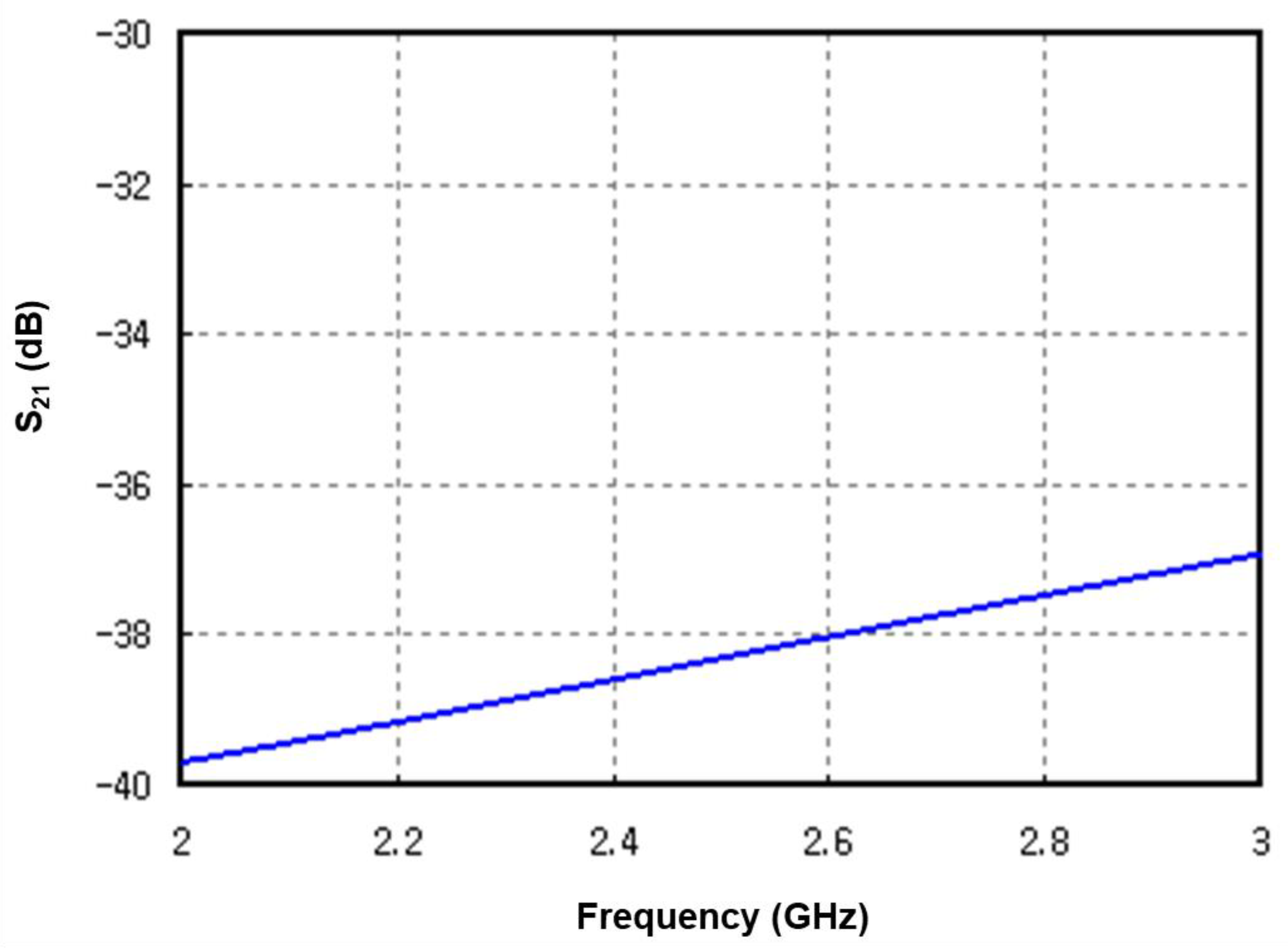
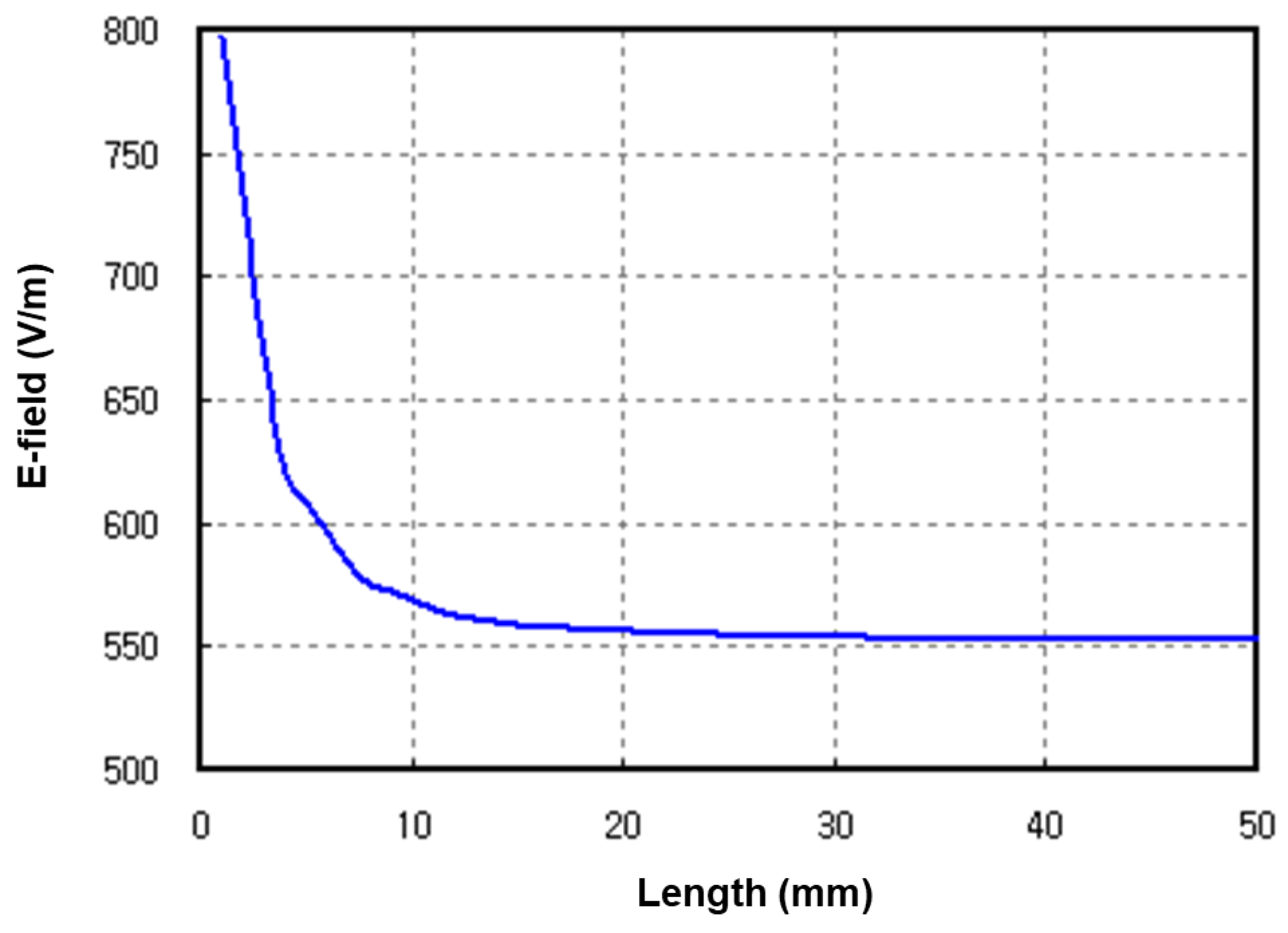
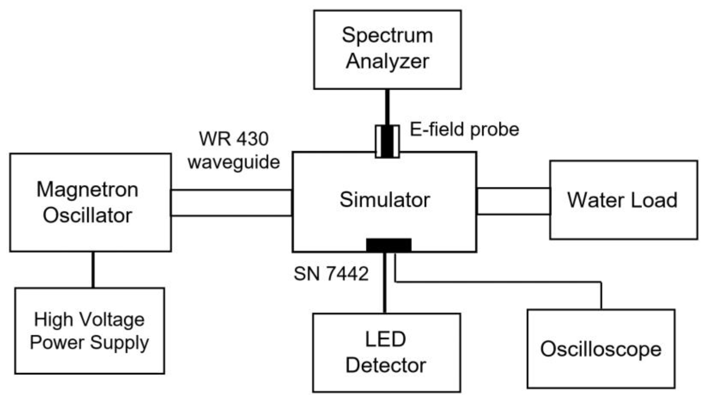
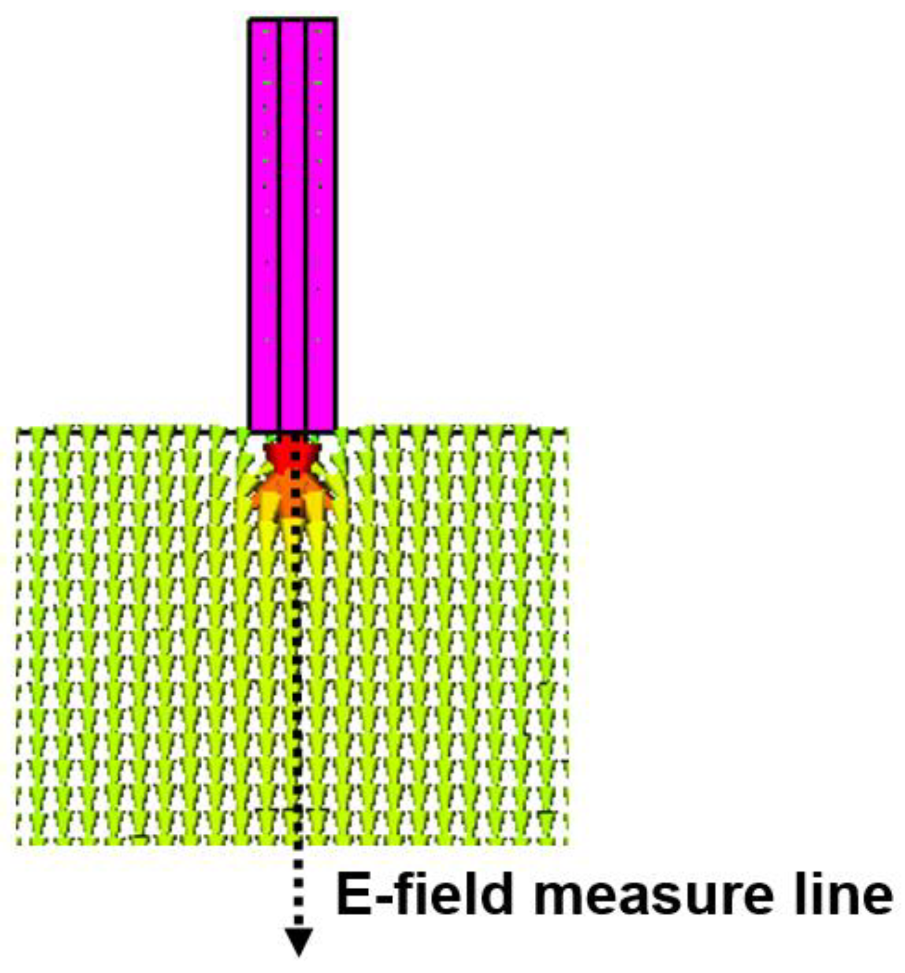
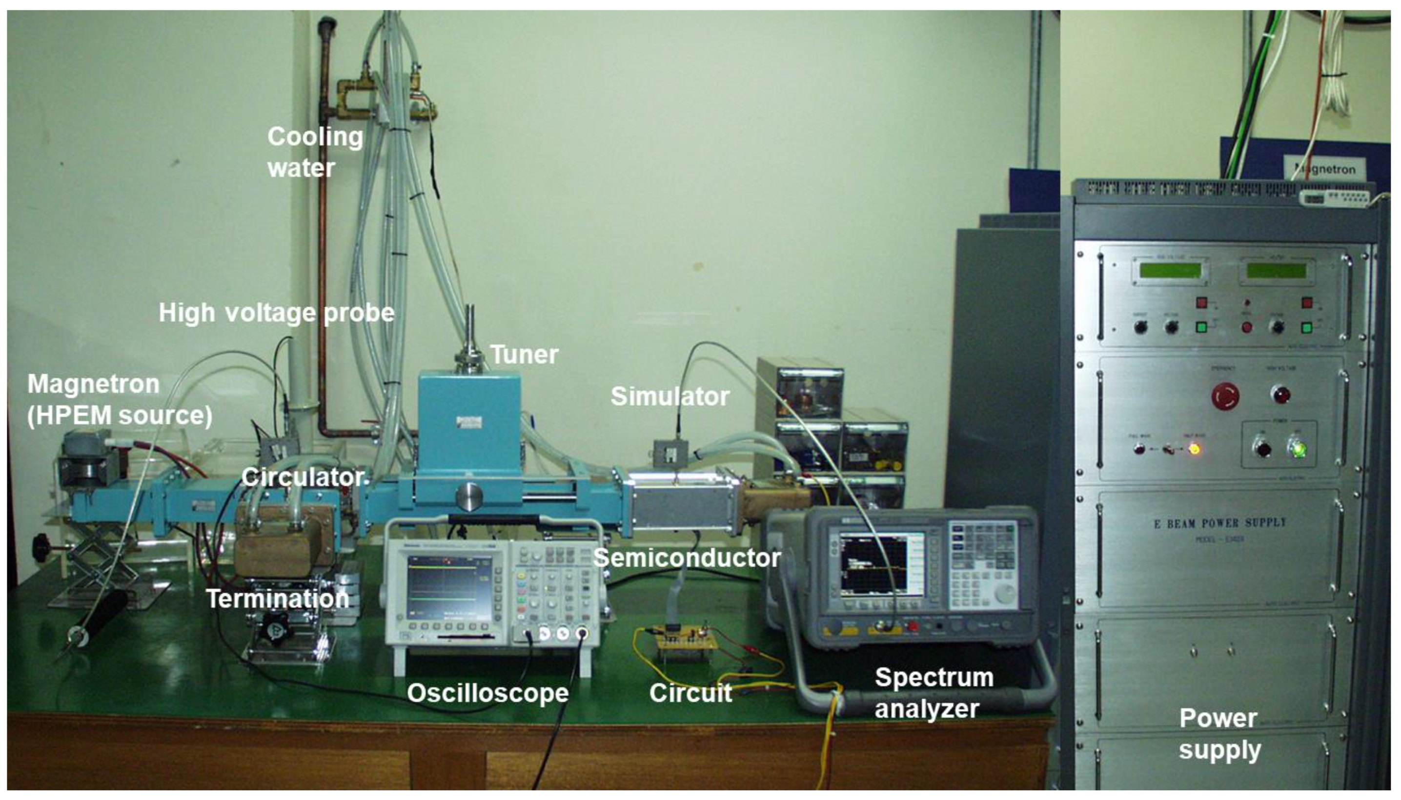
2. The WR430 Closed Waveguide Typed Emulator

The experimental setup used to measure the dependence of the irradiated HPEM on failure threshold time using a WR430 closed waveguide type of an emulator is shown in Figure 1. The WR430 closed waveguide emulator is located between a magnetron oscillator operated at 2.46 GHz as a HPEM source and the water load. The HPEM generated from the magnetron oscillator propagates along the WR430 waveguide and is irradiated into the semiconductor located at the bottom of the emulator [19,20,21,22,23].
The SN7442 IC is used in the experiment and functions to form a decimal code using a binary code. This is connected to a light-emitting diode (LED) detector which is turned on by the SN7442 IC, with the state of the SN7442, such as upset and destruction states, directly detected. To observe the time dependence caused by irradiated electric field, the voltage in the SN7442 IC is measured using an oscilloscope during the irradiation process. Using an E-field probe located on the upper side of the SN7442 IC, the magnitude of the irradiated electric field is measured.
The irradiated electric field is measured from the power coupling level between port 1 and port 2, as shown in Figure 2, using an E-field probe located on the upper side of the emulator. The E-field probe consisted of Teflon with a ϕ value of 4.1 mm and brass with a ϕ value of 1.26 mm. The relationship between the power coupling level and the magnitude of the irradiated electric field is expressed as follows. The charge induced in the central conductor of the E-field probe by the propagated electric field of E0 along the waveguide is expressed as Q i n = D · n ^ d a = ε o E o A e f f . The area of the induced charge is modified to the effective area, Aeff, due to the modification of the electric field near the central conductor of the E-field probe. The area of the induced charge is expressed as Aeff = KpA0. Here, A0 is the normal surface area of the central conductor in the E-field probe and Kp is the area multiplication factor, which indicates the entire modified area of the induced charge in the central conductor of the E-field probe. The induced current is I ( t ) = ε o ω E o K p A o e j ω t and the observed power in port 2 is expressed as P o b = 1 2 | I | 2 Z o = Z o 2 ( ε o ω E o K p A o ) 2 , where Z0 is the impedance of the E-field probe and ω is the HPEM frequency. This is re-expressed as
P o b = 2 ω μ o Z o P i n k z a b ( ε o ω K p A o ) 2
where Pin is the input power at port 1. Using the relationship between the observed power and the input power, the area multiplication factor is calculated as follows:
K p = 1 ε o ω A o k z a b P o b 2 ω μ o Z o P i n
From the measurement, Pob/Pin is measured and found to be −38.2 dB, and Kp is calculated as 26. Using Kp and Pob, the irradiated electric field is calculated where Z0 = 50 Ω.
E o = 1 ε o ω K p 2 P o b Z o
The electric field probe used to measure the electric field to be applied to the experimental semiconductor was designed using Microwave Studio, an electromagnetic (EM) simulation code, and the area multiplication factor equation discussed in relation to the relationship between the electromagnetic wave strength measured by the probe and the electric field. As shown in Figure 3, the emulator to be used in the experiment is composed of a closed waveguide. High-power electromagnetic waves generated by the magnetron, a high-power electromagnetic wave generator, are applied to Port 1 and pass through Port 3, with some of these waves detected by a probe located in Port 2. The detected output strength can be measured using a spectrum analyzer. At this time, the cross-section of the used electric field probe has a structure consisting of brass with a diameter of 1.26 mm in the center and Teflon with a diameter of 4.1 mm around it, as shown in Figure 3. Because the frequency component of the high-power electromagnetic wave generated by the magnetron is 2.45 GHz, a standard WR 430 waveguide served as the closed waveguide. The cross-sectional size of this waveguide is 54.6 mm × 109.2 mm. When an electromagnetic wave with a certain level of output strength is made to pass by using the electromagnetic simulation code, the output strength detected by the probe to be used in the experiment is measured, and the characteristics of the experimental devices can be compared.
The electric field distribution obtained using the EM simulation code is shown in Figure 4. When the electromagnetic wave generated by the magnetron passes through the WR 430 waveguide, it shows the electric field distribution of the TE10 mode, the most basic mode of the waveguide. The experimental semiconductor is located at the bottom of the waveguide, and the electric field probe is located directly above the semiconductor. This configuration allows the electric field applied to the semiconductor to be measured.
In order to measure the electric field strength applied to the semiconductor accurately, the ratio of the output strength detected by the probe from the waveguide must be measured accurately. Figure 5 shows the ratio of the measured output strength using a simulation for this purpose. This is to secure the reliability and reproducibility of the measurement and to stabilize the field-to-probe binding for a fixed length.
Figure 6 depicts the measurement line used to measure the strength of the electric field applied to the semiconductor via a simulation. Regarding the electric field in the area where the probe is located, it was determined to be slightly higher than the electric field strength at the bottom surface due to the influence of the center conductor of the probe; the influence of the probe disappears in the area outside the influence of the probe, meaning that only the electric field affected by the electromagnetic wave passing through the waveguide is measured.
Figure 7 shows the result of the measurement of the electric field strength in the area where the probe and semiconductor are located via the aforementioned simulation. The position of length = 0 is the position of the upper surface of the waveguide where the probe is located, and the position of length = 50 indicates the bottom of the waveguide where the semiconductor is located. It can be seen that the strength of the electric field in the region where the probe is located is greater than that in the region where the semiconductor is located due to the central conductor of the probe. However, because the influence of the probe does not affect the lower part where the semiconductor is located, it can be confirmed that an electric field of a certain size is applied to the semiconductor. The input strength of the electromagnetic wave used to obtain this result was 1 W, and the measured electric field strength was 552 V/m. The strength of the electric field at the input strength of 1 W obtained through the simulation can be compared with the theoretical value by examining the relationship between the input strength and the electric field. Given that the result is consistent with the theoretical value, the simulation result is reliable, and through this, the electric field probe was designed.

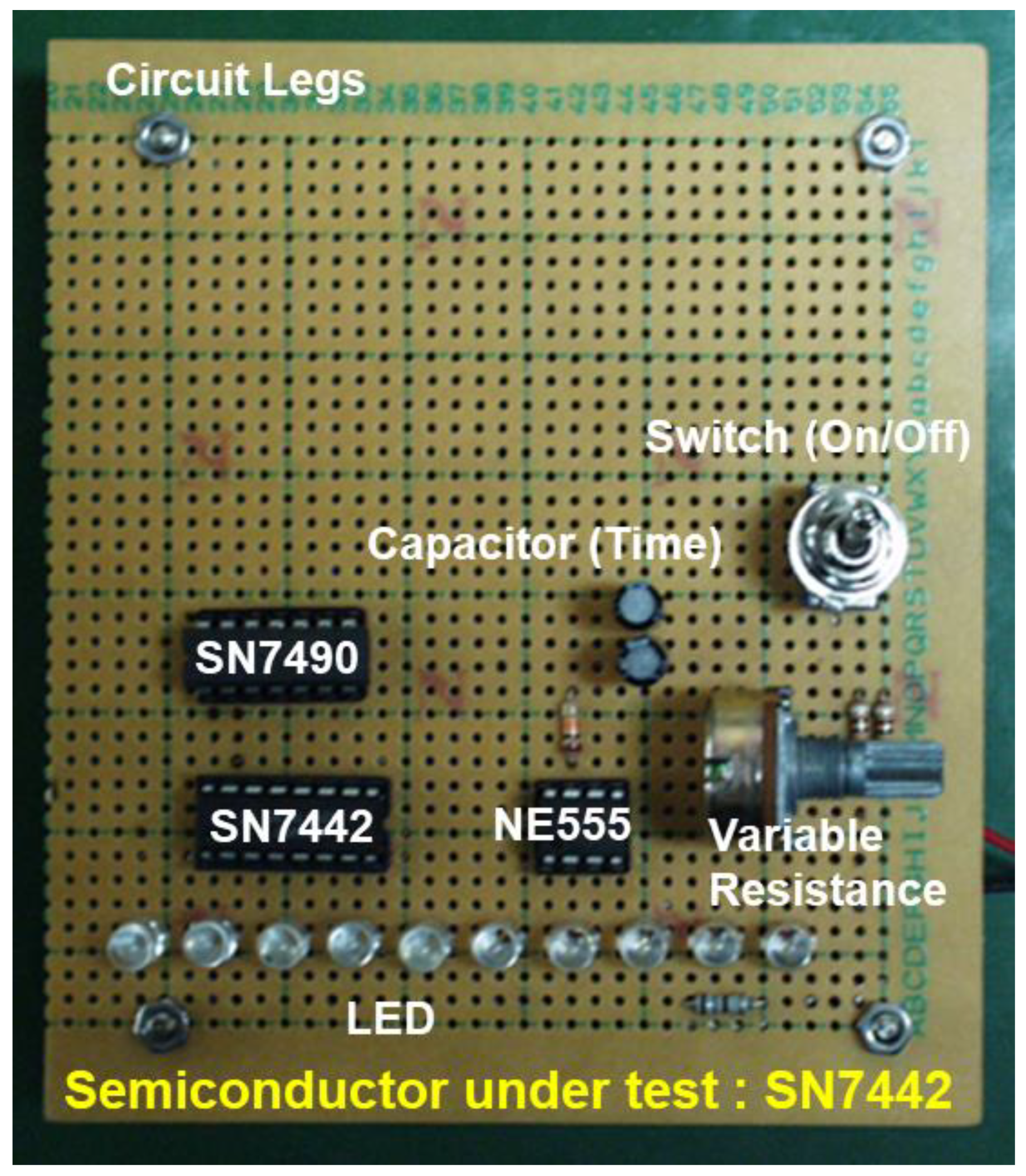
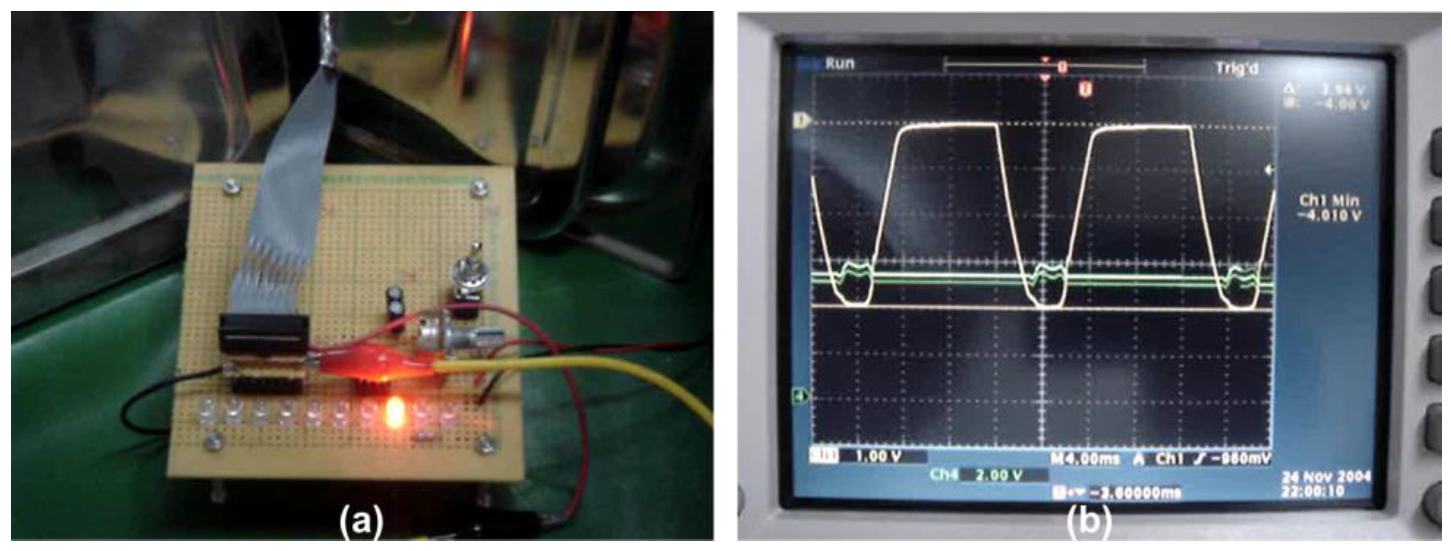
3. Experimental Setup

Figure 8 shows the configuration of the experimental apparatus used to obtain and analyze the destruction data of semiconductors exposed to intentionally generated high-power electromagnetic waves (HPEM). In order to create high-power transient electromagnetic waves intentionally, the magnetron, which is the HPEM source, is located on the left side of the experimental device, and the high-power electromagnetic waves generated from the magnetron are connected to the launcher and transmitted to the WR430 waveguide. They pass through the emulator and propagate to the termination point located at the right end. In order to eliminate heat generation due to the high-power electromagnetic waves, the termination point is structured to perform refrigeration using circulating cooling water.
The magnetron, a high-power electromagnetic wave generator, generates electromagnetic waves by applying voltage to the cathode that generates an electron beam and the anode that accelerates the generated electron beam. 4.5 V and 10A are applied to the cathode and voltage of 4 kV or more is applied to the anode. In this way, the magnetron can generate high-power electromagnetic waves at the desired output strength. A high voltage probe was used to measure the voltage applied to the magnetron from a high voltage power supply. It is equipped with an oscilloscope available to measure the voltage applied to the anode. Moreover, it can find the strength value of the electric field applied to the semiconductor through the electric field probe located on the upper part of the semiconductor. By coupling electromagnetic waves of a certain intensity level, it was possible to measure the electric field applied to the semiconductor with the measured output intensity using a spectrum analyzer.
Two methods were used to check for certain phenomena directly, such as upset/destruction phenomena that occur when high-power electromagnetic waves are applied to a semiconductor. First, in order to verify the characteristics of the high-power electromagnetic waves, we put the semiconductor in the experiment in the emulator and used a connection line to construct an LED circuit operated by the semiconductor while in the emulator. If an abnormality occurs in the semiconductor, the LED circuit operated by the semiconductor is abnormal. The upset/destruction characteristics can then be measured. Another measurement method used is to measure the voltage applied to the semiconductor in the emulator and to measure the applied voltage of the semiconductor, which changes when a high-power transient electromagnetic wave is applied. This allows its characteristics to be measured.
The emulator used in this experiment consists of a closed waveguide that supplies a uniform electric field to the experimental semiconductor. The lower surface of the waveguide has a groove for inserting the experimental semiconductor, and the electric field probe for measuring the electric field applied to the semiconductor is located on the upper surface at the same position so that the electric field used in the experiment can be measured.
Figure 9 shows the emulator arrangement, consisting of a closed waveguide. The emulator is located between two waveguides, which are in this case WR 430 waveguides that allow high-power electromagnetic waves generated by the magnetron to propagate through a certain area. The electric field probe is located at the top of the emulator, and an attenuator is connected to the probe to prevent strong electromagnetic waves from entering the spectrum analyzer.
In the emulator, a semiconductor for measuring the effects of electromagnetic waves is positioned, and the LED detector circuit driven due to the characteristics of the semiconductor is connected with a connection line so that the effect of the high-power electromagnetic waves on the semiconductor can be checked in real time. Moreover, as shown in the figure on the right side of Figure 9, the voltage applied to the semiconductor for the experiment was measured to determine how the applied electromagnetic wave affects the applied voltage characteristics of the semiconductor.
Figure 10 shows the circuit diagram of an LED detector configured to measure the change in the characteristics of semiconductors exposed to electromagnetic waves in the experiment. Three semiconductors (SN 7442, SN7490, NE555) were used to construct this circuit. The semiconductor exposed to the double electromagnetic waves is the SN7442 type; it receives a binary input signal and converts it to a decimal number and then turns on ten LEDs one after the other. When electromagnetic waves are not applied, the ten LEDs light up at regular intervals, and when electromagnetic waves are applied, the situation in which the LEDs are turned on without any tendency due to changes in certain characteristics (such as an upset event) can be directly observed through the LEDs. To measure the voltage applied to the semiconductor, the voltage V18 (the voltage signal required to operate LED 1) was measured using an oscilloscope, as shown in the Figure 10.
Figure 11 shows the LED detector circuit, which was devised based on the circuit diagram described in Figure 10. The characteristics of the semiconductor used in the circuit diagram are as follows. NE555 is applied to a non-stable multivibrator; this component is widely used as a pulse signal source for timer circuits and counter circuits. It can be used in TTL or CMOS circuits because it can operate in the DC voltage range of 4~15 V, and its rated current capacity is as large as 200 mA. The circuit used in the experiment supplies pulses to the counter (IC) SN7490.
The SN7490 component in Figure 12 is an IC with built-in binary and counter components. The clock pulse input of the binary counter is input A (#14) and the output is Qa (#12), and the clock pulse input of the pentagram counter is input B (#1) The outputs are Qb (#9), Qc (#8), and Qd (#11). Therefore, to use this as a BCD decimal counter, input A (#14) must be used as the clock pulse input, and Qa (#12) and input B (#1) must be connected before use. The outputs are Qa (#12), Qb (#9), Qc (#8), Qd (#11), but Qa is the lowest digit and Qd is the highest digit.
The SN7442 component in Figure 13 converts (decodes) the BCD output of the decimal counter (SN7490) to decimal and operates the corresponding LED. Therefore, the output LED turns on sequentially from No. 0 to No. 9. Table 1 below explains Qa~Qd.

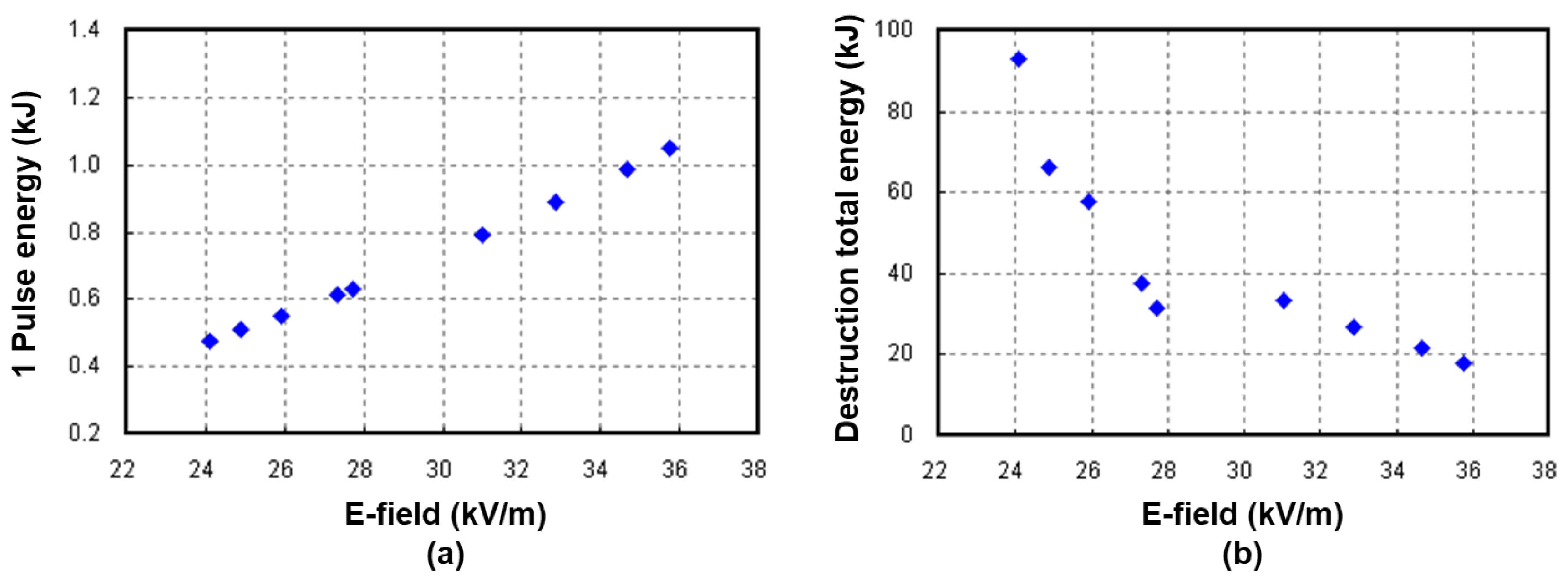
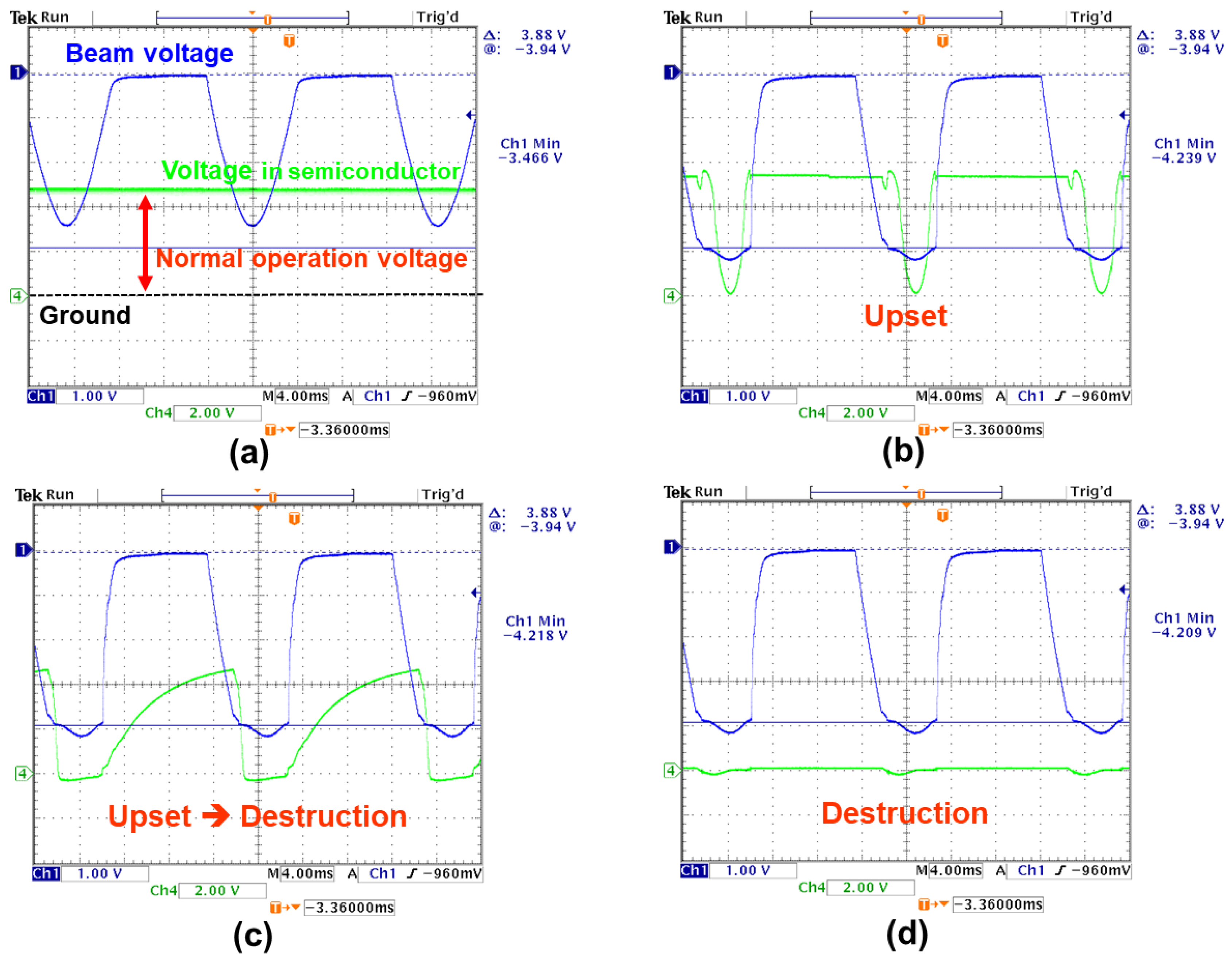
4. Experimental Results
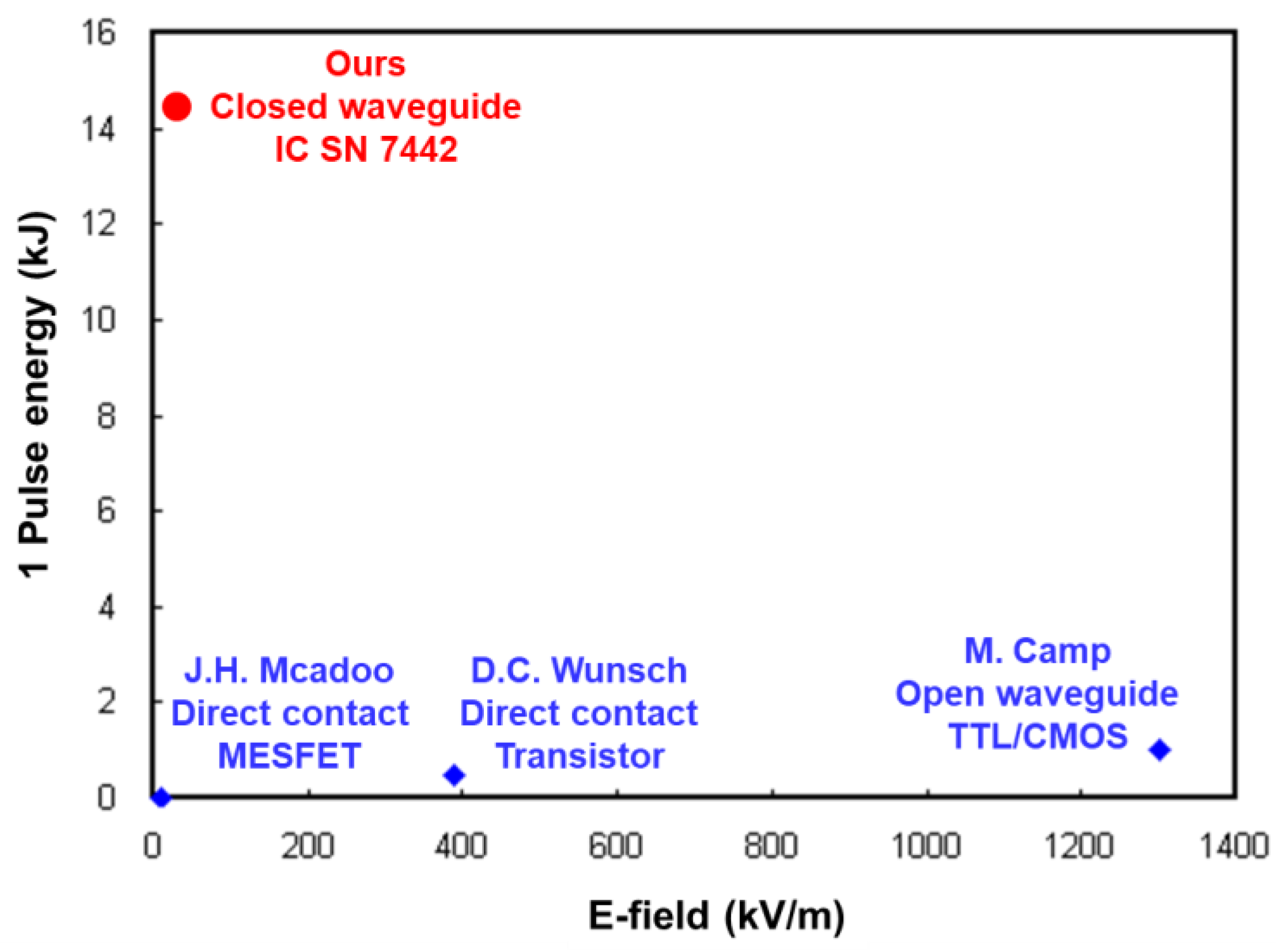
Figure 14a shows the LED detector in operation when a high-power electromagnetic wave is applied to a semiconductor. It can be observed that the operation of the LED changes as the intensity of the electromagnetic wave increases. Figure 14b presents the measurement of the voltage signal applied to the semiconductor with an oscilloscope when high-power electromagnetic waves are applied to the semiconductor.
When the high-power electromagnetic waves were applied to the semiconductor, the voltage signal applied to the semiconductor was measured, as shown in Figure 15a–d. Figure 15a shows the beam voltage and the voltage signal applied to the semiconductor before the high-power electromagnetic wave is applied, and Figure 15b is the beam voltage and the voltage signal applied to the semiconductor when the high-power electromagnetic wave is applied. Figure 15c indicates the beam voltage and the voltage signal applied to the semiconductor after a certain period of time has elapsed after the high-power electromagnetic wave is applied, as shown by the voltage signal.
As shown in Figure 15a, the measured part shown in blue represents the high voltage signal applied to the anode to drive the magnetron, and the measured part shown in green indicates the voltage applied to the semiconductor. This is a measure of the signal. As shown in Figure 15a, a certain voltage signal is applied to the semiconductor before the high-power electromagnetic wave is applied, and it operates normally. When the electromagnetic wave is applied, a situation in which the voltage signal of the semiconductor goes to 0 at the part where the electromagnetic wave is applied is noted, as shown in Figure 15b. This shows the conversion process. In Figure 15c, when high-power electromagnetic waves are applied for a certain period of time, the semiconductor is affected at the region where the electromagnetic waves are not applied such that the short-circuiting time becomes longer and the influence on the semiconductor lasts for a longer time. Figure 15d shows the time when the voltage signal is measured as zero at all times when the semiconductor is destroyed, and this indicates that the operation of the semiconductor does not recover again after the destruction.
Figure 16 shows the relationship between the destruction time of the semiconductor and the change in the output intensity generated by the magnetron, that is, the change in the electric field applied to the semiconductor. When the applied electric field changes from 24 kV/m to 36 kV/m, it can be observed that the destruction time decreases from 200 s to 15 s. Moreover, the greater the strength of the electric field applied to the semiconductor, that is, the greater the energy received by the semiconductor, the faster it is destroyed, and the relationship between the destruction time and the strength of the electric field can be divided into three regions based on a certain region. When region 1 is the region, when an electric field with low intensity is applied, the destruction time is proportional to −12 power of the electric field, and when region 2 is the region, when an electric field of about medium intensity is applied, the destruction time is proportional to the power of −10. Finally, region 3 is a region where a rather strong electric field is applied, and the destruction time is in proportion to −6 power of the electric field. This shows that the greater the electric field strength, the weaker the effect of the destruction time. Eventually, destruction of electronic devices exposed to high-power transient electromagnetic waves (HPEM) means physical damage and defines a case that can only be recovered through hardware replacement. The destruction time can be thought of in relation to the electric field, and it can be inferred that it is visually defined as a functional relationship with a tendency between the destruction time and threshold electric field, as shown in Figure 16.
Figure 17a,b are, correspondingly, graphs of one pulse energy according to the strength of the electric field and an electric graph according to the strength of the field. At a greater intensity of the electric field, that is, when the energy of one pulse is greater, less total energy that destroys the semiconductor can enter.
Figure 18 presents a comparison of the pulse energy according to the electric field strength with other experimental values, specifically those from J.H. Mcadoo and D.C Wunsch. In the Wunsch case, the energy of one pulse is shown when a DC pulse is applied using a line directly connected to the semiconductor. The experiment using the waveguide was devised by M. Camp with TTL/CMOS using an open waveguide. As shown in the M. Camp case, the electromagnetic wave used has a strong electric field of 1300 kV/m, but with a very short pulse. In this experiment with a closed waveguide, the strength of the electric field is weak, but a rather long pulse is used. In this experiment, the energy level is high.
Table 2 shows a comparison of each of the experiments related to transient electromagnetic waves. From the measured electric field strength, the condition of the electromagnetic wave required for the destruction of the semiconductor shows that the pulse width is short, whereas the strong electric field can cause destruction with little energy.

5. Discussion

In order to secure and analyze the threshold data of information devices exposed to high-power electromagnetic waves (HPEM), we reconfigured the HPEM environment to fit a suitable experimental environment for this. Through such a simulation, we intended to develop the emulator capable of measuring the level at which private information devices and systems are upset and/or destroyed by high-power transient electromagnetic waves, with the same effect considered accurately, as opposed to a study of an electromagnetic wave generator with the highest output at the gigawatt level. An electromagnetic wave generator with output power in the range of 1 W to 1 kW can be used. This basic research provides basic data for the development of emulators.
It is important to design an emulator consisting of a closed conduit that creates a uniform electric field for the investigations of the semiconductor component threshold characteristics. Here, it was designed/manufactured and used, and a magnetron with an operating frequency of 2.45 GHz and maximum output of 1 kW was used as the HPEM electromagnetic wave source. A breakdown/reset, destruction experiment, well known to influence the E-field, was designed with the corresponding control unit, a LED, and a power supply to measure the threshold while monitoring the operational status of the waveguide and an electronic device connecting the emulator and the electromagnetic wave in real time. In particular, this study analyzed and collected data by investigating the influence of semiconductor devices on the operating frequency, pulse duty, and electric field strength and direction.
As described above, as preliminary research on EMP protection methods and attacks, experimental research based on the emulator can be very important. The present study investigated the interaction between transient electromagnetic waves and semiconductor devices and examined conditions such as failures, damage, and malfunctions to determine the maximum degree of exposure to transient electromagnetic waves of sensitive communication devices. A database was compiled by experimenting with various types of semiconductor devices. Through a similar experiment on the communication equipment as a system, it can be possible to define the maximum transient electromagnetic wave allowed for all communication equipment. On the other hand, through the basic forms of this research, various hardening methods, such as shielding to minimize the effects of transient electromagnetic waves on semiconductors, can be developed.

6. Conclusions

In order to develop a technology to protect information equipment in response to the generation of high-power transient electromagnetic waves, a study of the effects on information equipment due to the generation of high-power transient electromagnetic waves must first be done first, which is what is presented here. In this study, a simulation was performed using a magnetron that generates an electromagnetic wave with an output of 1 kW at a frequency of 2.45 GHz. This was done in the laboratory of the authors in order to analyze the destructive effects by the E-field of a semiconductor component. Unlike previous, related studies, a closed waveguide was used for accurate experimental reproducibility and precise electric field measurements and control, and the data were collected and analyzed by measuring the threshold electric field affecting the semiconductor device. This research will provide basic data for the development of an HPEM emulator and the development of protection technology for information devices to secure them against high-power transient electromagnetic waves.

Author Contributions

Conceptualization, S.-H.M. and J.-I.K.; methodology, S.-H.M., J.-I.K. and C.P.; software, M.K. and S.M.; validation, K.-C.L. and Y.-J.L.; formal analysis, M.S., S.K. (Seontae Kim) and D.H.; investigation, S.K. (Seonmyeong Kim); resources, Y.-J.Y. and S.-Y.P.; data curation, S.-H.M., J.-I.K., M.S., H.-B.K. and C.P.; writing—original draft preparation, S.-H.M. and J.-I.K.; writing—review and editing, S.-H.M., J.-I.K., C.P., M.K., S.M., B.-H.H. and G.-S.P.; visualization, S.-H.M. and J.-I.K.; supervision, S.-H.M., J.-I.K., B.-H.H. and G.-S.P.; project administration, S.-H.M., J.-I.K., B.-H.H. and G.-S.P.; funding acquisition, S.-H.M., B.-H.H. and G.-S.P. All authors have read and agreed to the published version of the manuscript.

Funding

This work was supported by the National Research Foundation of Korea (NRF) grant funded by the Korea government (MSIP) (No. NRF—2021M2E8A1038938, No. NRF—2021R1F1A1048374, and No. NRF—2016R1A3B1908336). This study was also supported by a grant of the Korea Institute of Radiological and Medical Sciences (KIRAMS), funded by the Ministry of Science and ICT (MSIT), Republic of Korea. (No. 50051-2021, 50623-2021, and 50532-2021).

Data Availability Statement

The data that support the findings of this study are available from the corresponding author upon reasonable request.

Conflicts of Interest

The authors declare no conflict of interest.

References

  1. Olesen, H.L. Radiation Effects on Electronic Systems, 1st ed.; Springer: New York, NY, USA, 1966. [Google Scholar]
  2. Taylor, C.D.; Giri, D.V. High-Power Microwave Systems and Effects, 1st ed.; CRC Press: Boca Raton, FL, USA, 1994. [Google Scholar]
  3. Lee, K.S.H. EMP Interaction Principles, Techniques, and Reference Data, 1st ed.; Springer: Berlin/Heidelberg, Germany, 1986. [Google Scholar]
  4. James, B.; John, A.S.; Edl, S. High Power Microwaves, 3rd ed.; CRC Press: Boca Raton, FL, USA, 2016. [Google Scholar]
  5. Wunsch, D.C.; Bell, R.R. Determination of threshold failure levels of semiconductor diodes and transistors due to pulse voltages. IEEE Trans. Nucl. Sci. 1968, 15, 244–259. [Google Scholar] [CrossRef]
  6. McAdoo, J.H.; Bollen, W.M.; Catoe, W.; Kaul, R. Broad-band electromagnetic radiation damage in GaAs MESFETs. In Proceedings of the Microwave and Millimeter-Wave Monolithic Circuits Symposium 1992, San Diego, CA, USA, 10–13 May 1992; pp. 205–208. [Google Scholar]
  7. Camp, M.; Garbe, H.; Nitsch, D. Influence of the technology on the destruction effects of semiconductors by impact of EMP and UWB pulses. In Proceedings of the 2002 IEEE International Symposium on Electromagnetic Compatibility, Minneapolis, MN, USA, 19–23 August 2002; pp. 87–92. [Google Scholar]
  8. Camp, M.; Gerth, H.; Garbe, H.; Haase, H. Predicting the breakdown behavior of microcontrollers under EMP/UWB impact using a statistical analysis. IEEE Trans. Electromagn. Compat. 2004, 46, 368–379. [Google Scholar] [CrossRef]
  9. Sabath, F.; Giri, D.V.; Rachidi, F.; Kaelin, A. Ultra-Wideband, Short Pulse Electromagnetics 9, 1st ed.; Springer: Berlin/Heidelberg, Germany, 2010. [Google Scholar]
  10. Min, S.H.; Kwon, O.; Sattorov, M. Effects on electronics exposed to high-power microwaves on the basis of a relativistic backward wave oscillator operating on the X-band. J. Electromagn. Waves Appl. 2017, 31, 1875–1901. [Google Scholar] [CrossRef]
  11. Kesari, V.; Basu, B.N. High Power Microwave Tubes: Basics and Trends, 1st ed.; Morgan & Claypool Publishers: San Rafael, CA, USA, 2018. [Google Scholar]
  12. Zhen, K.; Shanwei, L.; Yan, Z.Y. Research on damage of intense electromagnetic pulse to radar receiving system. In Proceedings of the 2012 5th Global Symposium on Millimeter-Waves, Harbin, China, 27–30 May 2012; pp. 458–461. [Google Scholar]
  13. Military Standard. High-Altitude Electromagnetic Pulse (HEMP) Protection for Ground-Based C4I Facilities Performing Critical, Tine-Urgent Missions, Part 1 Fixed Facilities; MIL-STD-188-125-1; Department of Defense: Washington, DC, USA, 2005. [Google Scholar]
  14. Wilson, C. High Altitude Electromagnetic Pulse (HEMP) and High Power Microwave (HPM) Devices: Threat Assessments; CRS Report for Congress, 26 March 2008. 26 March 2008. Available online: https://www.everycrsreport.com/reports/RL32544.html (accessed on 2 August 2021).
  15. Giri, D.V.; Tesche, F.M. Classification of Intentional Electromagnetic Environments (IEME). IEEE Trans. Electromagn. Compat. 2004, 46, 322–328. [Google Scholar] [CrossRef]
  16. Kim, I.; Kovitz, J.M.; Rahmat-Samii, Y. Enhancing the Power Capabilities of the Stepped Septum Using an Optimized Smooth Sigmoid Profile. IEEE Trans. Antennas Propag. 2014, 56, 16–42. [Google Scholar] [CrossRef]
  17. Giri, D.V.; Hoad, R.; Sabath, F. High-Power Electromagnetic Effects on Electronic Systems, 1st ed.; Artech House: Boston, MA, USA, 2020. [Google Scholar]
  18. Zhang, J.; Zhang, D.; Fan, Y. Progress in narrowband high-power microwave sources. Phys. Plasmas. 2020, 27, 010501. [Google Scholar] [CrossRef]
  19. Kim, J.I.; Won, J.H.; Park, G.S. Numerical Study of a 10-Vane Strapped Magnetron Oscillator. J. Korean Phys. Soc. 2004, 44, 1229–1233. [Google Scholar]
  20. Jung, S.S.; Jin, Y.S.; Kim, J.I. Three-Dimensional Particle-in-Cell Simulations of a Strapped Magnetron Oscillator. J. Korean Phys. Soc. 2004, 44, 1250–1255. [Google Scholar]
  21. Kim, J.I.; Won, J.H.; Ha, H.J. Three-Dimensional Particle-in-Cell Simulation of 10-Vane Strapped Magnetron Oscillator. IEEE Trans. Plasma Sci. 2004, 32, 2099–2104. [Google Scholar] [CrossRef]
  22. Kim, J.I.; Won, J.H.; Park, G.S. Electron prebunching in microwave magnetron by electric priming using anode shape modification. Appl. Phys. Lett. 2005, 86, 171501. [Google Scholar] [CrossRef]
  23. Kim, J.I.; Won, J.H.; Park, G.S. Reduction of noise in strapped magnetron by electric priming using anode shape modification. Appl. Phys. Lett. 2006, 88, 221501. [Google Scholar] [CrossRef]
  24. LoVetri, J.; Wilbers, A.T.M.; Zwamborn, A.P.M. Microwave interaction with a personal computer: Experiment and modelling. In Proceedings of the 13th International Zurich Symposium Technical Exhibition on Electromagnetic Compatibility, Zurich, Switzerland, 16–18 February 1999; pp. 203–206. [Google Scholar]
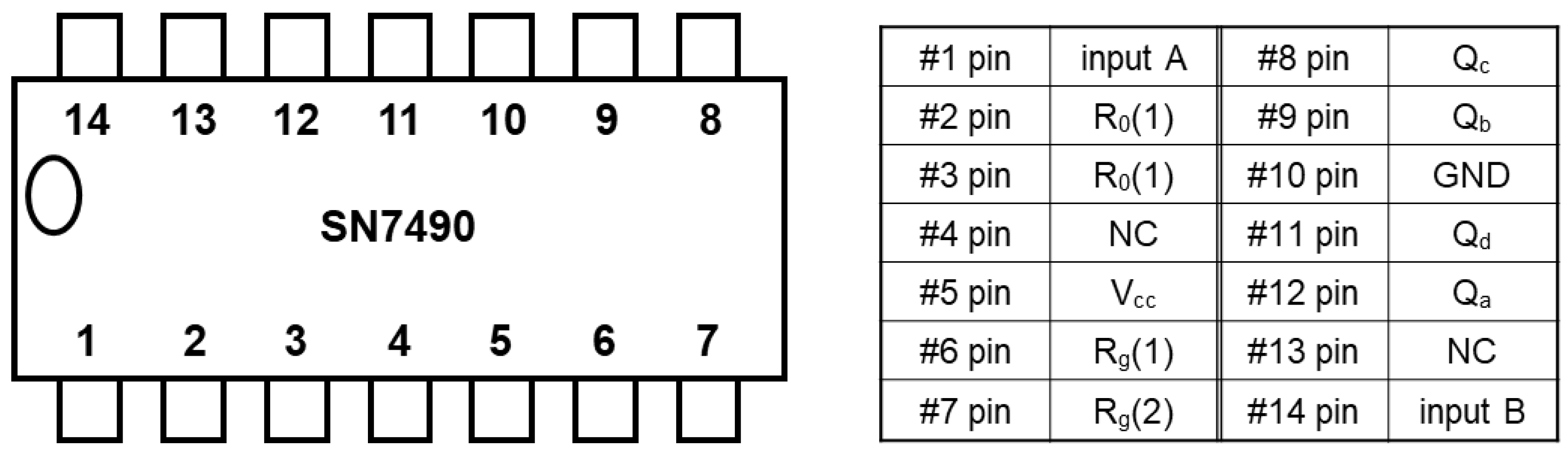
Figure 1. Experimental setup of the emulator equipped with a magnetron, and various fixtures.
Electronics 10 01884 g001
Figure 2. Design of the electric field probe.
Electronics 10 01884 g002
Figure 3. Simulation model for the electric-field probe design.
Electronics 10 01884 g003
Figure 4. Result of the electric-field distribution using the EM simulation code.
Electronics 10 01884 g004
Figure 5. Ratio of the power intensity coupled from the waveguide to the electric field probe.
Electronics 10 01884 g005
Figure 6. Ratio of the power intensity coupled from the waveguide to the electric field probe.
Electronics 10 01884 g006
Figure 7. Electric field in the area where the probe and semiconductor are located.
Electronics 10 01884 g007
Figure 8. An emulator and a magnetron-based high-power transient electromagnetic experiment device.
Electronics 10 01884 g008
Figure 9. An emulator setup consisting of a closed waveguide.
Electronics 10 01884 g009
Figure 10. Circuit diagram of the LED detector.
Electronics 10 01884 g010
Figure 11. Circuit of the LED detector.
Electronics 10 01884 g011
Figure 12. Characteristics of the SN7490 component.
Electronics 10 01884 g012
Figure 13. Characteristics of the SN7442 component.
Electronics 10 01884 g013
Figure 14. HPEM emulator experiment: (a) LED detector in operation, and (b) semiconductor voltage being measured.
Electronics 10 01884 g014
Figure 15. Voltage behavior in the semiconductor: (a) beam voltage before the high-power electromagnetic wave is applied and voltage signal applied to the semiconductor, (b) beam voltage when high-power electromagnetic waves start to be applied and voltage signals are applied to the semiconductor, (c) beam voltage and voltage signal applied to the semiconductor after a certain period of time after the high-power electromagnetic wave is applied, and (d) beam voltage and voltage signal applied to the semiconductor after the destruction of the semiconductor occurs after the application of the high-power electromagnetic waves.
Electronics 10 01884 g015
Figure 16. Destruction time as a function of the E–field.
Electronics 10 01884 g016
Figure 17. Destruction energy as a function of E-field; (a) one Pulse energy as a function of the E-field, (b) destruction total energy as a function of the E-field.
Electronics 10 01884 g017
Figure 18. Pulse energy comparison according to the electric field strength.
Electronics 10 01884 g018
Table 1. Input Pulses vs. Output for Qa~Qd.
Input PulseOutput
QdQcQbQa
00000
10001
20010
30011
40100
50101
60110
70111
81000
91001
Table 2. Comparison of Experiments Related to the HPEM Effect.
AuthorSemiconductor under TestExperimental MethodMeasured E-FieldResult
Wunsch, D.C. Ref. [5]TransistorDirect contactDestruction 500 kW/cm2 (390 kV/m) DC pulse~0.1 µsRelationship between the pulse width and the threshold power
Mcadoo, J.H. Ref. [6]MESFETDirect contactDestruction 400 W/cm2 (11 kV/m) DC pulse~0.086 µsRelationship between the DC pulse rise time and the damage voltage
Lovetri, J. Ref. [24]PCHorn antennaReset 32.9 mW/cm2 (100 V/m)The electric field region measurement for reset and power down scenarios
Camp, M. Ref. [7]TTL CMOSOpen waveguideDestruction 5.57 MW/cm2 (1300 kV/m), 0.18 µsRelationship between the E-field strength and the destruction rate
OursIC SN 7442Closed waveguideDestruction 31 kV/m (3.17 kW/cm2), 4 msRelationship between the E-field strength and the destruction time
Publisher’s Note: MDPI stays neutral with regard to jurisdictional claims in published maps and institutional affiliations.

