
Low-Power Multiplexer Structures Targeting Efficient QCA Nanotechnology Circuit Designs


Abstract
:1. Introduction
2. Methodology
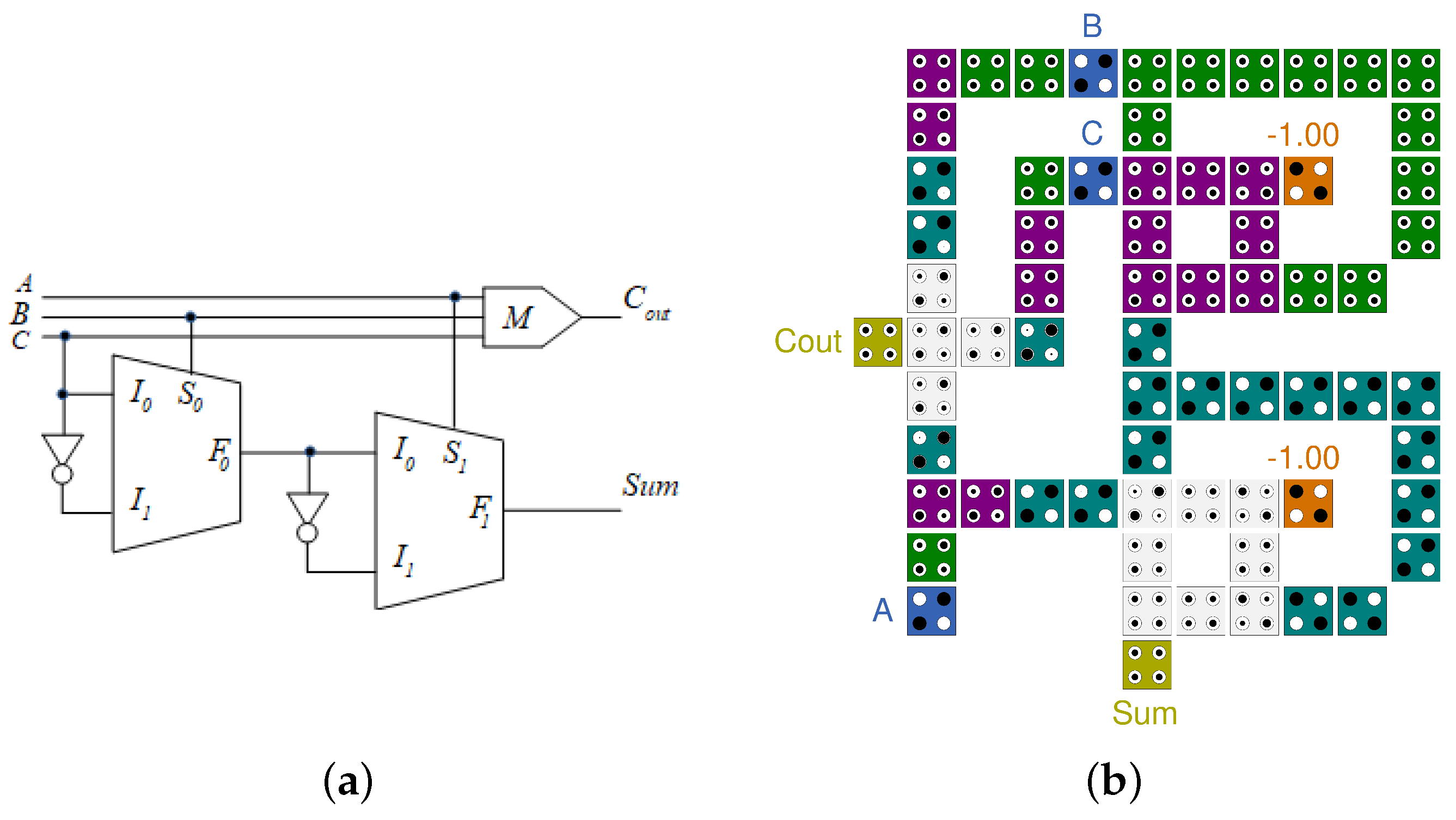
2.1. Proposed QCA Structures of a MUX
2.2. Basic Two-Input Functions Using the Proposed MUXes
2.3. Modularity Property
2.4. Further Designs Using MUX
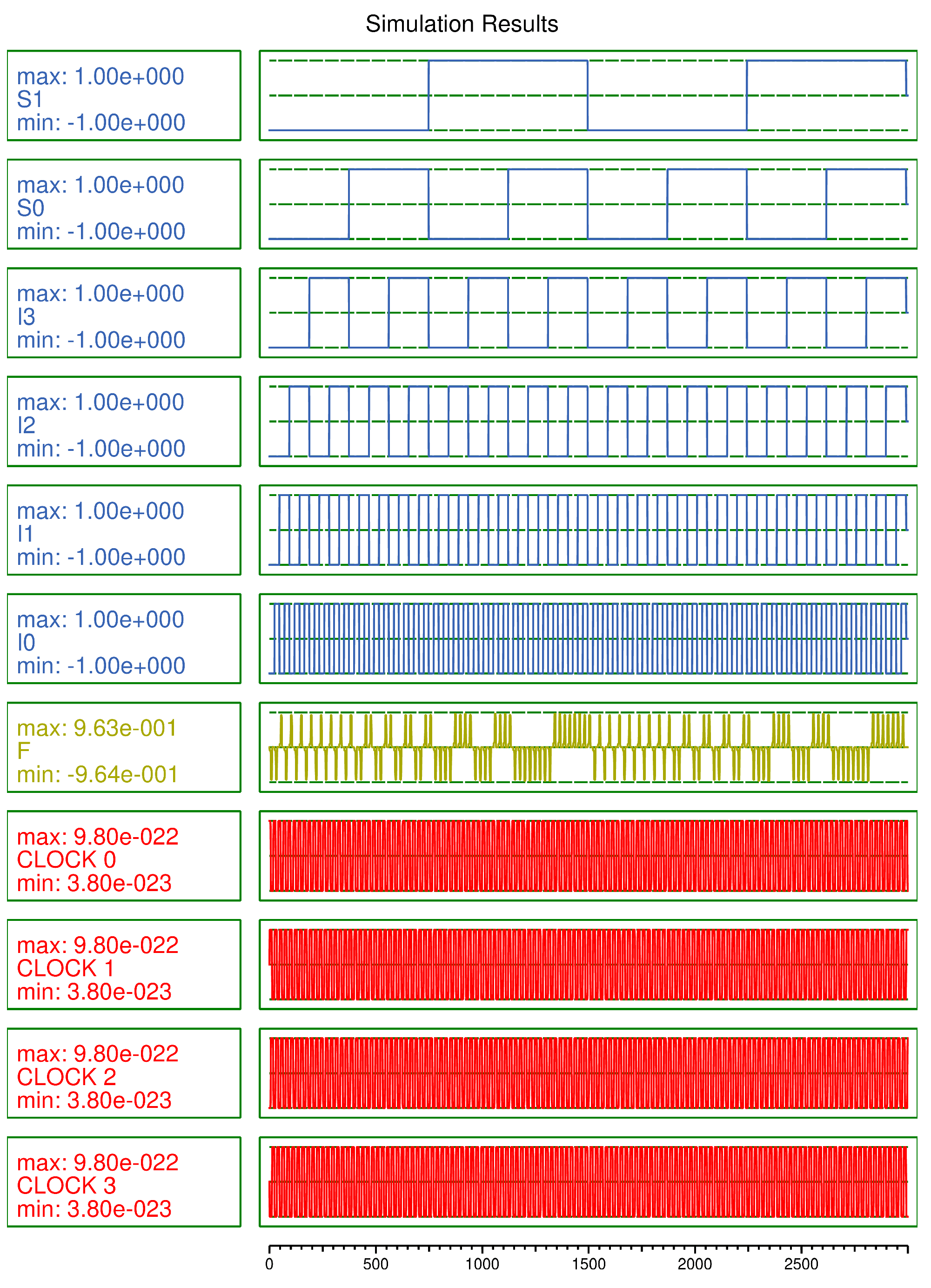
3. Simulation Results and Comparison
3.1. MUX Designs
3.2. MUX as a Fundamental Building Block for the Basic Two-Input Functions
3.3. MUX Design
4. Conclusions
Author Contributions
Funding
Conflicts of Interest
References
- 2013 International Technology Roadmap for Semiconductors (ITRS). 2013. Available online: https://www.semiconductors.org/resources/2013-international-technology-roadmap-for-semiconductors-itrs/ (accessed on 3 August 2021).
- Oya, T.; Asai, T.; Fukui, T.; Amemiya, Y. A majority-logic nanodevice using a balanced pair of single-electron boxes. J. Nanosci. Nanotechnol. 2002, 2, 333–342. [Google Scholar] [CrossRef] [PubMed]
- Oya, T.; Asai, T.; Fukui, T.; Amemiya, Y. A majority-logic device using an irreversible single-electron box. IEEE Trans. Nanotechnol. 2003, 2, 15–22. [Google Scholar] [CrossRef] [Green Version]
- Fahmy, H.A.H.; Kiehl, R.A. Complete logic family using tunneling-phase-logic devices. In Proceedings of the Eleventh International Conference on Microelectronics, ICM ’99, Safat, Kuwait, 22–24 November 1999; pp. 153–156. [Google Scholar] [CrossRef]
- Zahoor, F.; Hussin, F.A.; Khanday, F.A.; Ahmad, M.R.; Mohd Nawi, I.; Ooi, C.Y.; Rokhani, F.Z. Carbon nanotube field effect transistor (cntfet) and resistive random access memory (rram) based ternary combinational logic circuits. Electronics 2021, 10, 79. [Google Scholar] [CrossRef]
- Tabrizchi, S.; Panahi, A.; Sharifi, F.; Mahmoodi, H.; Badawy, A.H.A. Energy-Efficient Ternary Multipliers Using CNT Transistors. Electronics 2020, 9, 643. [Google Scholar] [CrossRef] [Green Version]
- Lent, C.S.; Tougaw, P.D.; Porod, W.; Bernstein, G.H. Quantum cellular automata. Nanotechnology 1993, 4, 49. [Google Scholar] [CrossRef]
- Tougaw, P.D.; Lent, C.S. Logical devices implemented using quantum cellular automata. J. Appl. Phys. 1994, 75, 1818–1825. [Google Scholar] [CrossRef]
- Lent, C.S.; Tougaw, P.D. A device architecture for computing with quantum dots. Proc. IEEE 1997, 85, 541–557. [Google Scholar] [CrossRef] [Green Version]
- Porod, W. Quantum-dot devices and quantum-dot cellular automata. Intern. J. Bifurc. Chaos 1997, 7, 2199–2218. [Google Scholar] [CrossRef] [Green Version]
- Snider, G.; Orlov, A.; Amlani, I.; Zuo, X.; Bernstein, G.; Lent, C.; Merz, J.; Porod, W. Quantum-dot cellular automata: Review and recent experiments. J. Appl. Phys. 1999, 85, 4283–4285. [Google Scholar] [CrossRef]
- Walus, K.; Jullien, G.A.; Dimitrov, V.S. Computer arithmetic structures for quantum cellular automata. In Proceedings of the Conference Record of the Thirty-Seventh Asilomar Conference on Signals, Systems & Computers, Pacific Grove, CA, USA, 9–12 November 2003; Volume 2, pp. 1435–1439. [Google Scholar] [CrossRef]
- AlKaldy, E.; Majeed, A.H.; Zainal, M.S.; Nor, D.M. Optimum multiplexer design in quantum-dot cellular automata. arXiv 2020, arXiv:2002.00360. [Google Scholar] [CrossRef]
- Sabbaghi-Nadooshan, R.; Kianpour, M. A novel QCA implementation of MUX-based universal shift register. J. Comput. Electron. 2014, 13, 198–210. [Google Scholar] [CrossRef]
- Sen, B.; Dutta, M.; Goswami, M.; Sikdar, B.K. Modular design of testable reversible ALU by QCA multiplexer with increase in programmability. Microelectron. J. 2014, 45, 1522–1532. [Google Scholar] [CrossRef]
- Rashidi, H.; Rezai, A.; Soltany, S. High-performance multiplexer architecture for quantum-dot cellular automata. J. Comput. Electron. 2016, 15, 968–981. [Google Scholar] [CrossRef]
- Asfestani, M.N.; Heikalabad, S.R. A unique structure for the multiplexer in quantum-dot cellular automata to create a revolution in design of nanostructures. Phys. B Condens. Matter 2017, 512, 91–99. [Google Scholar] [CrossRef]
- Song, Z.; Xie, G.; Cheng, X.; Wang, L.; Zhang, Y. An Ultra-Low Cost Multilayer RAM in Quantum-Dot Cellular Automata. IEEE Trans. Circuits Syst. II 2020, 67, 3397–3401. [Google Scholar] [CrossRef]
- Bahar, A.N.; Wahid, K.A. Design and Implementation of Approximate DCT Architecture in Quantum-Dot Cellular Automata. IEEE Trans. VLSI Syst. 2020, 28, 2530–2539. [Google Scholar] [CrossRef]
- Sen, B.; Goswami, M.; Mazumdar, S.; Sikdar, B.K. Towards modular design of reliable quantum-dot cellular automata logic circuit using multiplexers. Comput. Electr. Eng. 2015, 45, 42–54. [Google Scholar] [CrossRef]
- Sen, B.; Dutta, M.; Saran, D.; Sikdar, B.K. An efficient multiplexer in quantum-dot cellular automata. In Progress in VLSI Design and Test; Springer: Berlin/Heidelberg, Germany, 2012; pp. 350–351. [Google Scholar]
- Raj, M.; Gopalakrishnan, L.; Ko, S.B.; Naganathan, N.; Ramasubramanian, N. Configurable Logic Blocks and Memory Blocks for Beyond-CMOS FPGA-Based Embedded Systems. IEEE Embed. Syst. Lett. 2020, 12, 113–116. [Google Scholar] [CrossRef]
- Wang, L.; Xie, G. A Novel XOR/XNOR Structure for Modular Design of QCA Circuits. IEEE Trans. Circuits Syst. II 2020, 67, 3327–3331. [Google Scholar] [CrossRef]
- Safoev, N.; Jeon, J.C. Design and Evaluation of Cell Interaction Based Vedic Multiplier Using Quantum-Dot Cellular Automata. Electronics 2020, 5, 1036. [Google Scholar] [CrossRef]
- Babaie, S.; Sadoghifar, A.; Bahar, A.N. Design of an Efficient Multilayer Arithmetic Logic Unit in Quantum-Dot Cellular Automata (QCA). IEEE Trans. Circuits Syst. II 2019, 66, 963–967. [Google Scholar] [CrossRef]
- Bahar, A.N.; Wahid, K.A. Design of QCA-Serial Parallel Multiplier (QSPM) With Energy Dissipation Analysis. IEEE Trans. Circuits Syst. II 2020, 67, 1939–1943. [Google Scholar] [CrossRef]
- Abedi, D.; Jaberipur, G. Decimal Full Adders Specially Designed for Quantum-Dot Cellular Automata. IEEE Trans. Circuits Syst. II 2018, 65, 106–110. [Google Scholar] [CrossRef]
- Chu, Z.; Li, Z.; Xia, Y.; Wang, L.; Liu, W. BCD Adder Designs based on Three-Input XOR and Majority Gates. IEEE Trans. Circuits Syst. II 2020, 68, 1942–1946. [Google Scholar] [CrossRef]
- Seyedi, S.; Otsuki, A.; Navimipour, N.J. A New Cost-Efficient Design of a Reversible Gate Based on a Nano-Scale Quantum-Dot Cellular Automata Technology. Electronics 2021, 10, 1806. [Google Scholar] [CrossRef]
- Shannon, C.E. The synthesis of two-terminal switching circuits. Bell Syst. Tech. J. 1949, 28, 59–98. [Google Scholar] [CrossRef]
- Torres, F.S.; Wille, R.; Niemann, P.; Drechsler, R. An energy-aware model for the logic synthesis of quantum-dot cellular automata. IEEE Trans. Comput. Aided Des. Integr. Circuits Syst. 2018, 37, 3031–3041. [Google Scholar] [CrossRef]
- Bahar, A.N.; Wahid, K.A. Design of an efficient n × n butterfly switching network in quantum-dot cellular automata (QCA). IEEE Trans. Nanotechnol. 2020, 19, 147–155. [Google Scholar] [CrossRef]
- Vudadha, C.; Surya, A.; Agrawal, S.; Srinivas, M.B. Synthesis of Ternary Logic Circuits Using 2:1 Multiplexers. IEEE Trans. Circuits Syst. I 2018, 65, 4313–4325. [Google Scholar] [CrossRef]


| Function | Simplifications | QCA Implementation |
|---|---|---|
| AND |  | |
| OR |  | |
| NAND | 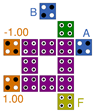 | |
| NOR | 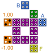 | |
| X-OR |  | |
| X-NOR |  |
| Parameter | Standard Value |
|---|---|
| Size of a quantum dot | 5 mm |
| Dimensions of each cell | 18 nm × 18 nm |
| Distance between two cells | 20 nm |
| Layer Separation | 11.5 nm |
| Operating temperature | 1 K |
| Relaxation time | s |
| Clock Period | s |
| Input Period | s |
| Time Step | s |
| Total simulation time | , * s |
| Max. saturation energy of clock signal | J |
| Min. saturation energy of clock signal | J |
| Clock Shift | 0 |
| Clock Slope | s |
| Shape of clock signal slopes | GAUSSIAN |
| Radius of Effect | 80 nm |
| Relative permittivity of material for QCA system | 12.9 |
| Circuit Design | Energy Dissipation (meV) with Respect to the Following Input Assignments () | Average Energy Dissipation (meV) | Area (µm2) | Clock Zones | |||||||
|---|---|---|---|---|---|---|---|---|---|---|---|
| 000 | 001 | 010 | 011 | 100 | 101 | 110 | 111 | ||||
| Proposed MUX1 (2 zones) | 0.328 | 0.175 | 0.307 | 0.649 | 0.409 | 1.278 | 0.328 | 0.889 | 0.545 | 0.01 | 2 |
| Proposed MUX1 (1 zone) | 0.347 | 0.193 | 0.327 | 0.783 | 0.542 | 1.326 | 0.443 | 1.003 | 0.621 | 0.01 | 1 |
| Proposed MUX2 (2 zones) | 0.492 | 0.407 | 0.356 | 0.180 | 1.278 | 0.479 | 0.176 | 0.465 | 0.479 | 0.01 | 2 |
| Proposed MUX2 (1 zone) | 0.607 | 0.522 | 0.490 | 0.201 | 1.327 | 0.612 | 0.194 | 0.483 | 0.554 | 0.01 | 1 |
| [13] (b) * | 0.361 | 0.208 | 0.340 | 1.581 | 0.904 | 1.102 | 0.785 | 1.265 | 0.818 | 0.01 | 2 |
| [13] (c) * | 1.076 | 1.515 | 1.029 | 1.488 | 0.418 | 2.170 | 0.907 | 1.764 | 1.296 | 0.01 | 2 |
| [14] | 1.182 | 1.291 | 1.273 | 0.709 | 0.811 | 1.305 | 0.855 | 0.725 | 1.019 | 0.02 | 2 |
| [20] | 0.802 | 1.487 | 1.371 | 0.876 | 0.697 | 2.095 | 1.263 | 1.484 | 1.259 | 0.02 | 2 |
| [15] | 1.045 | 1.937 | 0.972 | 0.900 | 0.965 | 1.945 | 0.890 | 0.908 | 1.195 | 0.02 | 2 |
| [21] | 1.284 | 1.793 | 1.815 | 0.918 | 0.724 | 2.331 | 1.275 | 1.449 | 1.449 | 0.02 | 3 |
| [16] | 0.363 | 1.334 | 0.361 | 0.734 | 0.796 | 1.343 | 0.792 | 0.752 | 0.809 | 0.01 | 2 |
| [17] | 0.743 | 0.845 | 0.508 | 0.638 | 0.719 | 0.876 | 0.688 | 0.878 | 0.737 | 0.01 | 1 |
| [18] | 1.049 | 0.778 | 1.043 | 1.054 | 0.784 | 0.783 | 0.780 | 1.064 | 0.917 | 0.01 | 2 |
| [19] | 0.762 | 1.550 | 0.274 | 0.405 | 1.417 | 1.544 | 1.427 | 0.896 | 1.034 | 0.01 | 2 |
| [31] | 2.477 | 1.285 | 2.282 | 2.476 | 1.911 | 2.233 | 1.713 | 2.208 | 2.073 | 0.09 | 5 |
| [22] | 1.782 | 1.687 | 1.718 | 0.910 | 0.848 | 1.701 | 0.743 | 0.926 | 1.290 | 0.01 | 2 |
| Function | Circuit-Based Design | Energy Dissipation (meV) with Respect to the Following Input Assignments () | Average Energy Dissipation (meV) | Area (µm2) | Clock Zones | |||
|---|---|---|---|---|---|---|---|---|
| 00 | 01 | 10 | 11 | |||||
| AND | Proposed MUX1 | 0.2784 | 0.1243 | 0.2566 | 0.5860 | 0.3113 | 0.01 | 2 |
| Proposed MUX2 | 0.2702 | 0.9271 | 0.1922 | 0.3688 | 0.4396 | 0.01 | 2 | |
| Majority [31] | 0.2962 | 0.9880 | 0.8646 | 0.3708 | 0.6299 | 0.01 | 2 | |
| OR | Proposed MUX1 | 0.3663 | 0.1995 | 0.8484 | 0.3836 | 0.4495 | 0.01 | 2 |
| Proposed MUX2 | 0.2989 | 0.1266 | 0.1252 | 0.4129 | 0.2409 | 0.01 | 2 | |
| Majority [31] | 0.3056 | 0.9979 | 0.8762 | 0.6801 | 0.7150 | 0.01 | 2 | |
| NAND | Proposed MUX1 | 0.2905 | 0.1723 | 0.2005 | 0.1640 | 0.2068 | 0.01 | 3 |
| Proposed MUX2 | 0.1735 | 0.1688 | 1.1841 | 0.3552 | 0.4704 | 0.01 | 3 | |
| Majority [31] | 0.3891 | 1.0825 | 0.9573 | 0.4559 | 0.7212 | 0.02 | 3 | |
| NOR | Proposed MUX1 | 0.3546 | 1.1847 | 0.1678 | 0.1745 | 0.4704 | 0.01 | 3 |
| Proposed MUX2 | 0.1599 | 0.2023 | 0.1685 | 0.2942 | 0.2062 | 0.01 | 3 | |
| Majority [31] | 0.3892 | 1.0783 | 1.0095 | 0.5079 | 0.7462 | 0.02 | 3 | |
| X-OR | Proposed MUX1 | 0.5495 | 0.4482 | 0.4381 | 1.4901 | 0.7315 | 0.02 | 3 |
| Proposed MUX2 | 0.3851 | 0.7173 | 1.4229 | 0.4929 | 0.7545 | 0.02 | 3 | |
| Majority [31] | 1.8431 | 2.9851 | 2.6477 | 1.4990 | 2.2437 | 0.09 | 6 | |
Publisher’s Note: MDPI stays neutral with regard to jurisdictional claims in published maps and institutional affiliations. |
© 2021 by the authors. Licensee MDPI, Basel, Switzerland. This article is an open access article distributed under the terms and conditions of the Creative Commons Attribution (CC BY) license (https://creativecommons.org/licenses/by/4.0/).
Share and Cite
Almatrood, A.; George, A.K.; Singh, H. Low-Power Multiplexer Structures Targeting Efficient QCA Nanotechnology Circuit Designs. Electronics 2021, 10, 1885. https://doi.org/10.3390/electronics10161885
Almatrood A, George AK, Singh H. Low-Power Multiplexer Structures Targeting Efficient QCA Nanotechnology Circuit Designs. Electronics. 2021; 10(16):1885. https://doi.org/10.3390/electronics10161885
Chicago/Turabian StyleAlmatrood, Amjad, Aby K. George, and Harpreet Singh. 2021. "Low-Power Multiplexer Structures Targeting Efficient QCA Nanotechnology Circuit Designs" Electronics 10, no. 16: 1885. https://doi.org/10.3390/electronics10161885
APA StyleAlmatrood, A., George, A. K., & Singh, H. (2021). Low-Power Multiplexer Structures Targeting Efficient QCA Nanotechnology Circuit Designs. Electronics, 10(16), 1885. https://doi.org/10.3390/electronics10161885