Article

Effects of Active Layer Thickness on the Electrical Characteristics and Stability of High-Mobility Amorphous Indium–Gallium–Tin Oxide Thin-Film Transistors

School of Electrical and Electronics Engineering, Chung-Ang University, Seoul 06974, Korea
*
Author to whom correspondence should be addressed.
Co-first author, these authors contributed equally to this work.
Electronics 2021, 10(11), 1295; https://doi.org/10.3390/electronics10111295
Submission received: 22 April 2021 / Revised: 21 May 2021 / Accepted: 27 May 2021 / Published: 28 May 2021
(This article belongs to the Special Issue Applications of Thin Films in Microelectronics)

Abstract

:
Herein, we investigated the effects of active layer thickness (tS) on the electrical characteristics and stability of high-mobility indium–gallium–tin oxide (IGTO) thin-film transistors (TFTs). IGTO TFTs, with tS values of 7 nm, 15 nm, 25 nm, 35 nm, and 50 nm, were prepared for this analysis. The drain current was only slightly modulated by the gate-to-source voltage, in the case of the IGTO TFT with tS = 50 nm. Under positive bias stress (PBS), the electrical stability of the IGTO TFTs with a tS less than 35 nm improved as the tS increased. However, the negative bias illumination stress (NBIS) stability of these IGTO TFTs deteriorated as the tS increased. To explain these phenomena, we compared the O1s spectra of IGTO thin films with different tS values, acquired using X-ray photoelectron spectroscopy. The characterization results revealed that the better PBS stability, and the low NBIS stability, of the IGTO TFTs with thicker active layers were mainly due to a decrease in the number of hydroxyl groups and an increase in the number of oxygen vacancies in the IGTO thin films with an increase in tS, respectively. Among the IGTO TFTs with different tS, the IGTO TFT with a 15-nm thick active layer exhibited the best electrical characteristics with a field-effect mobility (µFE) of 26.5 cm2/V·s, a subthreshold swing (SS) of 0.16 V/dec, and a threshold voltage (VTH) of 0.3 V. Moreover, the device exhibited robust stability under PBS (ΔVTH = 0.9 V) and NBIS (ΔVTH = −1.87 V).

1. Introduction

Amorphous indium–gallium–zinc oxide (IGZO) thin-film transistors (TFTs) were reported for the first time by Nomura et al. in 2004; since, they have attracted significant attention because of their excellent electrical properties, low process temperature, large-area uniformity, and low fabrication cost [1,2,3,4,5]. Currently, IGZO TFTs are being widely used as a backplane for large-area active-matrix flat-panel displays, such as organic light-emitting diode (OLED) displays and liquid-crystal displays (LCD) [6,7,8]. The recent development of low-temperature polysilicon oxide technology is expected to further expand the application range of IGZO TFTs in the field of displays [7,8]. However, the relatively low field-effect mobility of IGZO TFTs (µFE = ~10 cm2/V·s) still hinders their application in the backplane of ultra-high-resolution and high-frame-rate displays [9,10]. This is because the OLED pixels require a high current to emit light. Therefore, the study presents a new low-voltage driving OLED pixel circuit with high-mobility amorphous oxide TFTs as the driving device with high resolution [11]. To date, various oxide semiconductors have been studied as active materials for high-mobility oxide TFTs [12,13,14]. Among them, IGTO has recently attracted considerable attention as a promising active material for next-generation high-mobility oxide TFTs. The In3+ and Sn4+ ions have almost similar electronic structures. They have a small effective electron mass due to the 5 s orbital overlapping structure, leading to a highly conductive path for electron carriers, and remarkably high mobility [15,16]. Furthermore, the IGTO TFTs exhibit excellent electrical characteristics, even at low annealing temperatures (below 200 °C) [17,18,19].
For oxide TFTs, active layer thickness (tS) is an important parameter that strongly affects the electrical performance and stability of these TFTs. To date, extensive research has been performed to determine the effects of tS on the electrical characteristics and stability of oxide TFTs comprising different active materials. However, previous studies have reported different results for the effects of tS on the electrical characteristics and stability of oxide TFTs according to the type of active material and fabrication process conditions. For example, Cho et al. [20] and Yang et al. [21] reported that the positive bias stress (PBS) stability of indium–zinc-oxide and IGZO TFTs deteriorated with an increase in tS, respectively. Nevertheless, Lee et al. [22] and Li et al. [23] observed an improvement in the PBS stability of IGZO TFTs with an increase in tS. These results imply that investigating the effects of tS on the electrical performance and stability of IGTO TFTs is extremely necessary to determine the optimal tS for IGTO TFTs. In this study, we examined the effects of tS on the electrical characteristics and stability of IGTO TFTs. IGTO TFTs, with the tS values of 7 nm, 15 nm, 25 nm, 35 nm, and 50 nm, were prepared for this analysis. A systematic study was conducted to investigate the physical mechanisms responsible for the observed effects of tS on the electrical performance and PBS/NBIS stability of IGTO TFTs.

2. Materials and Methods

Figure 1a,b shows the schematic and top-view optical image of the fabricated IGTO TFTs, respectively. The IGTO TFTs were constructed on a heavily doped p-type Si wafer (resistivity < 0.005 Ω · cm) covered by 100-nm thick thermally grown SiO2. The heavily doped p-type Si wafer was used as a substrate and a gate electrode. Thermally grown SiO2 was used as a gate dielectric. IGTO active layers with the thicknesses of 7 nm, 15 nm, 25 nm, 35 nm, and 52 nm were deposited on the substrate by direct current magnetron sputtering under the following conditions: working pressure, 3.0 mTorr, Ar/O2; gas mixing ratio, 21/9 sccm; sputtering power, 150 W; and chuck temperature, room temperature (RT). Then, a 100-nm thick indium–tin-oxide layer was deposited on the IGTO active layer-coated substrate to prepare source and drain electrodes of the TFTs. Subsequently, a 30-nm thick Al2O3 thin film was deposited as a passivation layer on top of the resulting substrate using radio frequency magnetron sputtering at RT. Finally, the IGTO TFTs were thermally annealed on a hot plate at 200 °C for 2 h in ambient air.
The active, source/drain electrodes, and passivation layers were patterned using photolithography and a lift-off process. Electrical characteristics and stability of the IGTO TFTs were measured using a semiconductor parameter analyzer (4156C, Agilent Technologies, Santa Clara, CA, USA) at RT in ambient air. Crystalline structure of the IGTO thin films was analyzed using X-ray diffraction (XRD, New D8-Advance, Bruker-AXS, Wisconsin, USA) with CuKα radiation (λ = 0.15406 nm). Chemical properties of the IGTO thin films with different tS were examined using X-ray photoelectron spectroscopy (XPS, K-alpha+, Thermo Fisher Scientific-KR, Seoul, Korea). An Ar ion beam was employed to sputter the Al2O3 and IGTO thin films before XPS characterization.

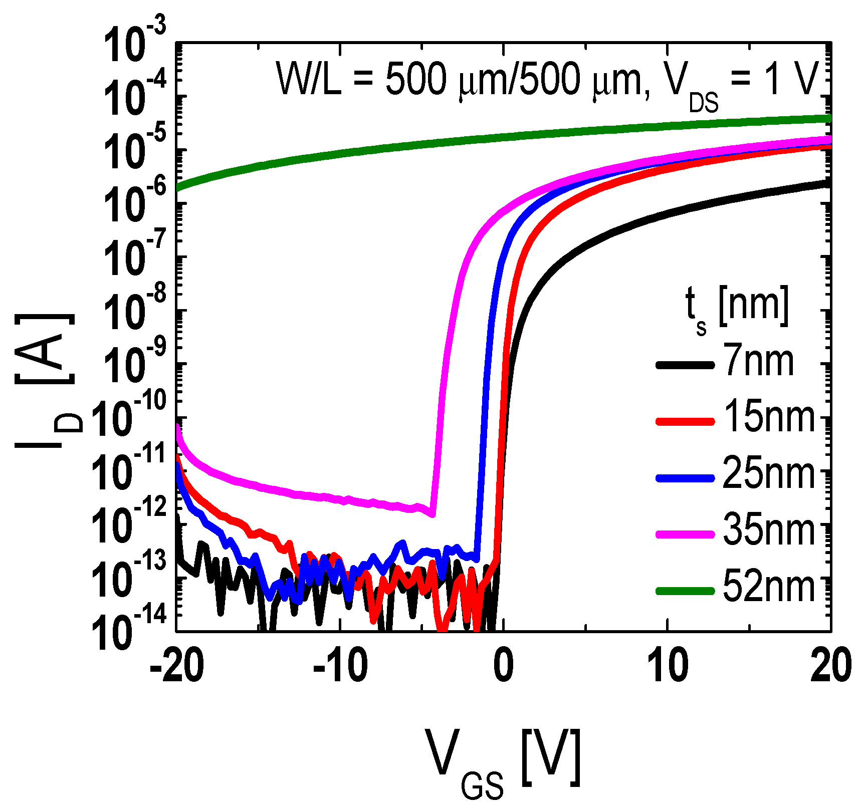
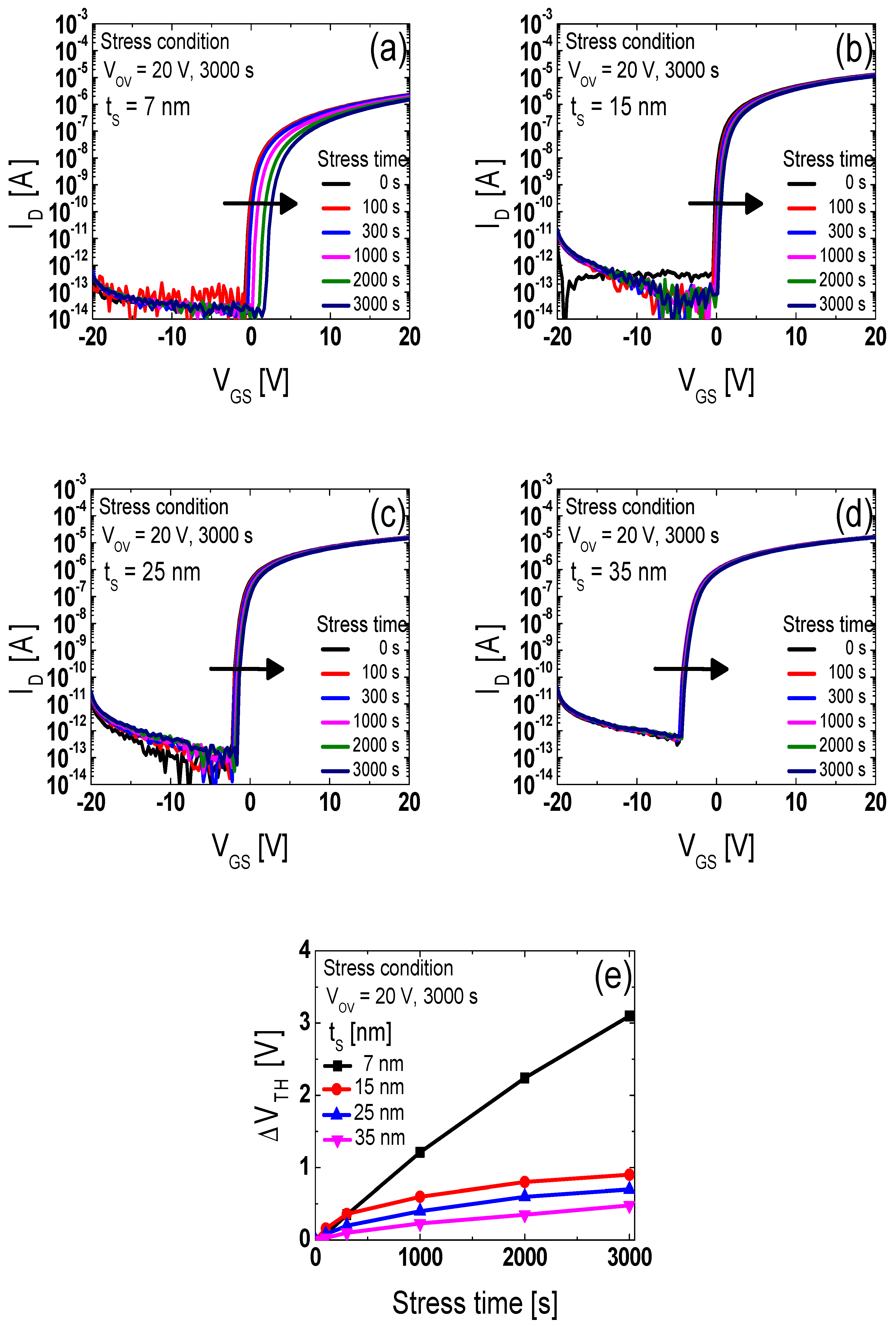
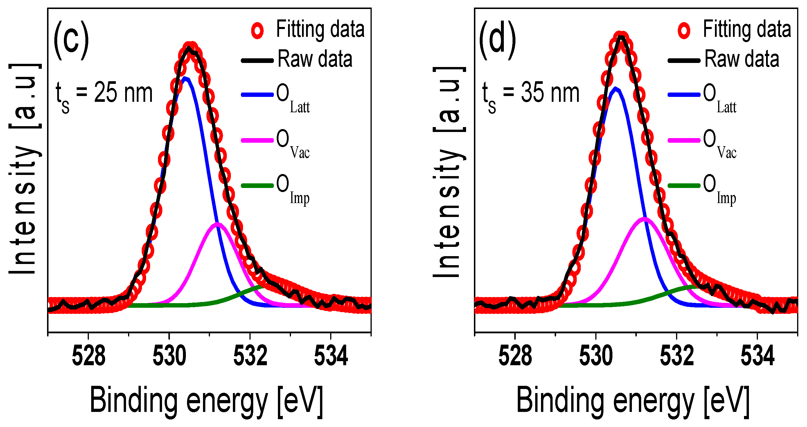
3. Results and Discussion

Figure 2 shows the XRD patterns of a 35-nm thick IGTO thin film fabricated on an aluminosilicate glass substrate. The XRD pattern demonstrates only halo peaks at approximately 23° and 45°, originating from the glass substrate [24]. The results shown in Figure 2 indicate that the IGTO thin film has an amorphous phase, which is consistent with the results of previous studies [17].
Figure 3 shows a semi-logarithmic scale plot of transfer curves for the IGTO TFTs (width/length (W/L) = 500 μm/500 μm), with the tS of 7, 15, 25, 35, and 50 nm. Herein, the drain current (ID) of all of the IGTO TFTs was evaluated by varying the gate-to-source voltage (VGS) from −20 to 20 V at a fixed drain-to-source voltage (VDS) of 1 V. Figure 3 shows that the ID of the IGTO TFT with a tS of 50 nm is slightly modulated by VGS; therefore, the electrical characteristics and stability of only the IGTO TFTs with the tS of 7, 15, 25, and 35 nm were examined in this study. Table 1 presents the electrical parameters of the IGTO TFTs with the tS of 7, 15, 25, and 35 nm. The µFE was calculated using the maximum value of transconductance, and the VTH was determined as the VGS value causing ID = W/L × 10−8 (A) at a VDS of 1 V. The subthreshold swing (SS) was extracted as the d(VGS)/d(logID) value in the range of 10−10 A < ID < 10−9 A. The VTH decreased and the SS and the off-current (IOFF) increased with an increase in tS (Figure 3 and Table 1). The IGTO TFT with the tS of 7 nm exhibited a significantly smaller µFE than those of the IGTO TFTs with thicker active layers. However, the µFE of the IGTO TFTs with a tS larger than 15 nm only slightly increased with an increase in tS. The results shown in Figure 3 and Table 1 are consistent with those reported in previous studies for oxide TFTs, and they demonstrate that tS significantly affects the transfer characteristics of IGTO TFTs [25]. The negatively shifted VTH and the large SS for the thick active oxide TFTs have been mainly attributed to the large number of free electrons within the oxide semiconductor and the higher sheet trap density in the active layer, respectively [26,27,28]. The increase in IOFF with an increase in tS was considered to be due to enhanced bulk conduction through the back-active layer [27]. The increase in μFE with an increase in tS has been primarily ascribed to the reduced surface roughness scattering in the oxide semiconductor. As the carrier transport layer is farther from the surface of the thick film, the effect of the surface roughness on the carrier mobility is weaker in the thick film, compared with the thin film [29,30].
Figure 4a–d shows the time dependence of the transfer curves for the IGTO TFTs with the tS of 7, 15, 25, and 35 nm, respectively, at a VOV (VOV = VGSVTH) of 20 V and a VDS of 0 V. For every IGTO TFT, the transfer curves shifted in the positive direction with an increase in the stress time. The largest shift in VTHVTH) was observed for the IGTO TFT with the tS of 7 nm (ΔVTH = 3.1 V after stress for 3000 s), whereas the smallest ΔVTH was noticed for the IGTO TFT with the tS of 35 nm (ΔVTH = 0.5 V after stress for 3000 s). Figure 4e depicts the ΔVTH for the IGTO TFTs with different tS under PBS at different stress times. Clearly, the magnitude of ΔVTH for the fabricated IGTO TFTs decreased with an increase in tS under PBS (Figure 4).
Figure 5a–d shows the time dependence of the transfer curves for the IGTO TFTs with the tS of 7, 15, 25, and 35 nm, respectively, at a VOV of −20 V and a VDS of 0 V, under illumination using a white light-emitting diode (LED, wavelength 420–780 nm) backplane unit with a luminance of 2000 lux. For every IGTO TFT, the transfer curves shifted in the negative direction with an increase in the stress time. The largest magnitude of ΔVTH was obtained for the IGTO TFT with the tS of 35 nm (ΔVTH = −11.2 V after stress for 3000 s), whereas the smallest magnitude of ΔVTH was achieved for the IGTO TFT with the tS of 7 nm (ΔVTH = −0.6 V after stress for 3000 s). Figure 5e depicts the ΔVTH for the IGTO TFTs with different tS under negative bias illumination stress (NBIS) at different stress times. The magnitude of ΔVTH for the fabricated IGTO TFTs increased with an increase in tS under NBIS (Figure 5).
To investigate the physical mechanisms responsible for the effects of tS on the PBS and NBIS stability of IGTO TFTs (Figure 4 and Figure 5), we characterized the O1s spectra of the IGTO thin films with different tS obtained using XPS. Figure 6a–d shows the XPS O1s spectra of 7, 15, 25, and 35-nm thick IGTO thin films located near the IGTO/SiO2 interface. The XPS O1s spectra were resolved into three sub-peaks originating from fully coordinated metal ions (metal–oxygen lattice (OLatt)), oxygen vacancies (OVac), and impurity-related oxygen (OImp). The XPS peak positions assigned to these sub-peaks were 530.0 eV (OLatt), 531.0 eV (OVac), and 532.5 eV (OImp), respectively [14,17]. Figure 7 shows the relative peak area ratios of OLatt, OVac, and OImp for the IGTO thin films with different tS, located near the IGTO/SiO2 interface. The relative peak area ratio of OImp was highest for the 7-nm thick IGTO thin film, and decreased with an increase in tS (Figure 7). In previously reported studies on IGZO or IGTO TFTs, OImp was mainly ascribed to the O bond in the hydroxyl group (OH) [17]. The OH creates acceptor-like trap states close to the conduction band (CB) edge and accelerates the electron trapping process under PBS because of its polar nature [17,31,32,33,34]. Considering this, the lower PBS stability of the IGTO TFTs with thinner active layers can be ascribed to the high concentration of OH in the channel layer. It has been reported that a thicker active layer can isolate the channel from ambient factors, including H2O molecules, even after the passivation layer is deposited on the active layer [35]. Effective self-passivation from H2O molecules in the air is the most probable reason for the better PBS stability of the IGTO TFTs with thicker active layers (Figure 7).
Figure 7 also shows that the relative peak area ratio of OVac is the smallest for the 7-nm thick IGTO thin film, and it increases with an increase in tS. OVac are easily created by sputtering-induced damage in oxide semiconductors [27,36]. Therefore, the concentration of OVac in IGTO increases with an increase in tS because of the longer sputtering time. OVac generates shallow and deep donor states in oxide semiconductors such as IGZO and IGTO [37,38]. Under NBIS, OVac is ionized to OVac2+, and OVac2+ drifts toward the oxide semiconductor/gate dielectric interface in oxide TFTs [39]. The increased concentration of electrons, and the formation of an OVac2+ accumulation layer near the gate, dielectric shifts the transfer curves of the TFTs in the negative direction [40]. The obtained results show that the lower NBIS stability of the IGTO TFTs with thicker active layers can possibly be attributed to the higher concentration of OVac in the IGTO thin film, caused by the more severe sputtering-induced damage. The experimental results shown in Figure 4 and Figure 5 indicate that it is necessary to consider the trade-off between the PBS and NBIS stability of the devices, while determining the optimum tS for IGTO TFTs. From the transfer characteristics and PBS/NBIS stability of the IGTO TFTs with different tS, it can be concluded that 15 nm is the optimal tS for IGTO TFTs, leading to the best electrical characteristics (µFE: 26.5 cm2/V·s; SS: 0.16 V/dec; and VTH: 0.3 V), and decent PBS and NBIS stability of IGTO TFTs.

4. Conclusions

In this study, we examined the effects of tS on the transfer characteristics and stability of high-mobility amorphous IGTO TFTs with tS values of 7, 15, 25, 35, and 50 nm. The obtained results showed that with an increase in tS, VTH shifted in the negative direction, and the SS and µFE of the fabricated IGTO TFTs increased. Clearly, the PBS stability of the IGTO TFTs improved as the tS increased. However, the NBIS stability of the IGTO TFTs deteriorated with an increase in tS. The XPS characterization results revealed that the better PBS stability and the low NBIS stability of the IGTO TFTs with thicker active layers were mainly owing to the decrease in the concentration of OH and the increase in the number of OVac in the IGTO, with an increase in tS. We found that the optimum thickness of the active layer for the IGTO TFTs is approximately 15 nm, which results in a positive VTH, an acceptably high µFE, and decent PBS and NBIS stability of the IGTO TFTs.

Author Contributions

Conceptualization, D.-H.K., H.-S.C. and H.-I.K.; experiment, H.-S.J., H.-S.C. and S.-H.H.; data analysis, D.-H.K. and H.-I.K., writing—original draft preparation, D.-H.K.; supervision, H.-I.K.; and writing—review and editing, H.-I.K. All authors have read and agreed to the published version of the manuscript.

Funding

This research was supported by the National Research Foundation of Korea (NRF) grant funded by the Korean government (MSIT) (No. 2019M3F3A1A03079821) and the Chung-Ang University Research Scholarship Grants in 2017. The authors would like to thank Dr. Shinhyuk Kang (Samsung Corning Advanced Glass) for providing the IGTO sputter target for this study.

Conflicts of Interest

The authors declare no conflict of interest.

References

  1. Nomura, K.; Ohta, H.; Takagi, A.; Kamiya, T.; Hirano, M.; Hosono, H. Room-temperature fabrication of transparent flexible thin-film transistors using amorphous oxide semiconductors. Nature 2004, 432, 488–492. [Google Scholar] [CrossRef]
  2. Fortunato, E.; Barquinha, P.; Martins, R. Oxide semiconductor thin-film transistors: A review of recent advances. Adv. Mater. 2012, 24, 2945–2986. [Google Scholar] [CrossRef] [PubMed]
  3. Kamiya, T.; Hosono, H. Material characteristics and applications of transparent amorphous Oxide semiconductors. NPG Asia Mater. 2010, 2, 15–22. [Google Scholar] [CrossRef] [Green Version]
  4. Jang, J.T.; Ahn, G.H.; Choi, S.-J.; Kim, D.M.; Kim, D.H. Control of the boundary between the gradual and abrupt modulation of resistance in the schottky barrier tunneling-modulated amorphous Indium-Gallium-Zinc-Oxide memristors for neuromorphic computing. Electronics 2019, 8, 1087. [Google Scholar] [CrossRef] [Green Version]
  5. Park, J.-S.; Maeng, W.-J.; Kim, H.-S.; Park, J.-S. Review of recent developments in amorphous Oxide semiconductor thin-film transistor devices. Thin Solid Films 2012, 520, 1679–1693. [Google Scholar] [CrossRef]
  6. Kikuchi, Y.; Nomura, K.; Yanagi, H.; Kamiya, T.; Hirano, M.; Hosono, H. Device characteristics improvement of a-In–Ga–Zn–O TFTs by low-temperature annealing. Thin Solid Films 2010, 518, 3017–3021. [Google Scholar] [CrossRef]
  7. Rahaman, A.; Jeong, H.; Jang, J. A High-Gain CMOS Operational Amplifier Using Low-Temperature Poly-Si Oxide TFTs. IEEE Trans. Electron Devices 2020, 67, 524–527. [Google Scholar] [CrossRef]
  8. Jeong, D.Y.; Chang, Y.; Yoon, W.G.; Do, Y.; Jang, J. Low-Temperature Polysilicon Oxide Thin-Film Transistors with Coplanar Structure Using Six Photomask Steps Demonstrating High Inverter Gain of 264 V V−1. Adv. Eng. Mater. 2020, 22, 1901497. [Google Scholar] [CrossRef]
  9. Kim, S.-C.; Jeon, Y.-W.; Kim, Y.-S.; Kong, D.-S.; Jung, H.-K.; Bae, M.-K.; Lee, J.-H.; Ahn, B.-D.; Park, S.-Y.; Park, J.-H.; et al. Impact of oxygen flow rate on the instability under positive bias stresses in DC-sputtered amorphous InGaZnO thin-film transistors. IEEE Electron Device Lett. 2012, 33, 62–64. [Google Scholar] [CrossRef]
  10. Yabuta, H.; Sano, M.; Abe, K.; Aiba, T.; Den, T.; Kumomi, H.; Nomura, K.; Kamiya, T.; Hosono, H. High mobility thin-film transistor with amorphous InGaZnO4 channel fabricated by room temperature rf magnetron sputtering. Appl. Phys. Lett. 2006, 89, 112123. [Google Scholar] [CrossRef]
  11. Fan, C.L.; Tsao, H.Y.; Chen, C.Y.; Chou, P.C.; Lin, W.Y. New Low-Voltage Driving Compensating Pixel Circuit Based on HighMobility Amorphous Indium-Zinc-Tin-Oxide Thin-Film Transistors for High-Resolution Portable Active-Matrix OLED Displays. Coatings 2020, 10, 1004. [Google Scholar] [CrossRef]
  12. Fuh, C.-S.; Liu, P.-T.; Huang, W.-H.; Sze, S.M. Effect of annealing on defect elimination for high mobility amorphous Indium-Zinc-Tin-Oxide thin-film transistor. IEEE Electron Device Lett. 2014, 35, 1103. [Google Scholar] [CrossRef]
  13. Paine, D.-C.; Yaglioglu, B.; Beiley, Z.; Lee, S.-H. Amorphous IZO-based transparent thin film transistor. Thin Solid Films 2008, 516, 5894–5898. [Google Scholar] [CrossRef]
  14. Ruan, D.-B.; Liu, P.-T.; Chiu, Y.-C.; Kan, K.-Z.; Yu, M.-C.; Chien, T.-C.; Chen, Y.-H.; Kuo, P.-Y.; Sze, S.-M. Investigation of low operation voltage InZnSnO thin-film transistors with dierent high-k gate dielectric by physical vapor deposition. Thin Solid Films 2018, 660, 885–890. [Google Scholar] [CrossRef]
  15. Noh, J.-Y.; Kim, H.; Nahm, H.-H.; Kim, Y.-S.; Kim, D.H.; Ahn, B.-D.; Lim, J.-H.; Kim, G.H.; Lee, J.-H.; Song, J. Cation composition effects on electronic structures of In-Sn-Zn-O amorphous semiconductors. J. Appl. Phys. 2013, 113, 3706-1–3706-7. [Google Scholar] [CrossRef] [Green Version]
  16. Kim, B.K.; On, N.; Choi, C.H.; Kim, M.J.; Kang, S.; Lim, J.H.; Jeong, J.K. Polycrystalline Indium Gallium Tin Oxide Thin-Film Transistors With High Mobility Exceeding 100 cm2/V·s. IEEE Electron Device Lett. 2021, 42, 347–357. [Google Scholar] [CrossRef]
  17. Jeong, H.-S.; Cha, H.S.; Hwang, S.H.; Kwon, H.-I. Effects of annealing atmosphere on electrical performance and stability of high-mobility Indium-Gallium-Tin Oxide thin-film transistors. Electronics 2020, 9, 1875. [Google Scholar] [CrossRef]
  18. Hur, J.-S.; Kim, J.-O.; Kim, H.-A.; Jeong, J.-K. Stretchable polymer gate dielectric by ultraviolet-assisted Hafnium Oxide doping at low temperature for high-performance Indium Gallium Tin Oxide transistors. ACS Appl. Mater. Interfaces 2019, 11, 21675–21685. [Google Scholar] [CrossRef] [PubMed]
  19. Kim, J.-O.; Hur, J.-S.; Kim, D.-S.; Lee, B.-M.; Jung, J.-M.; Kim, H.-A.; Chung, U.-J.; Nam, S.-H.; Hong, Y.T.; Park, K.-S.; et al. Network structure modification-enabled hybrid polymer dielectric film with Zirconia for the stretchable transistor applications. Adv. Funct. Mater. 2020, 30, 1906647. [Google Scholar] [CrossRef]
  20. Cho, E.N.; Kang, J.H.; Yun, I. Effects of channel thickness variation on bias stress instability of InGaZnO thin-film transistors. Microelectron. Reliab. 2011, 51, 1792–1795. [Google Scholar] [CrossRef]
  21. Yang, Z.; Yang, J.; Meng, T.; Qu, M.; Zhang, Q. Influence of channel layer thickness on the stability of amorphous indium zinc oxide thin film transistors. Mater. Lett. 2016, 166, 46–50. [Google Scholar] [CrossRef]
  22. Lee, S.Y.; Kim, D.H.; Chong, E.; Jeon, Y.W.; Kim, D.H. Effect of channel thickness on density of states in amorphous InGaZnO thin film transistors. Appl. Phys. Lett. 2011, 98, 122105-1–122105-3. [Google Scholar] [CrossRef] [Green Version]
  23. Li, G.T.; Yang, B.R.; Liu, C.; Lee, C.Y.; Tseng, C.Y.; Lo, C.C.; Lien, A.; Deng, S.Z.; Shieh, H.P.D.; Xu, N.S. Positive gate bias instability alleviated by self-passivation effect in amorphous InGaZnO thin-film transistors. J. Phys. D Appl. Phys. 2015, 48, 475107. [Google Scholar] [CrossRef]
  24. Jung, S.H.; Moon, H.J.; Ryu, M.K.; Cho, K.I.; Bae, B.S.; Yun, E.-J. The effects of high-energy electron beam irradiation on the properties of IGZO thin films prepared by rf magnetron sputtering. J. Ceram. Process. Res. 2012, 13, s246–s250. [Google Scholar]
  25. Shin, M.-G.; Hwang, S.-H.; Cha, H.-S.; Jeong, H.-S.; Kim, D.-H.; Kwon, H.-I. Effects of proton beam irradiation on the physical and chemical properties of IGTO thin films with different thicknesses for thin-film transistor applications. Surf. Interfaces 2021, 23, 100990. [Google Scholar] [CrossRef]
  26. Barquinha, P.; Pimentel, A.; Marques, A.; Pereira, L.; Martins, R.; Fortunato, E. Influence of the semiconductor thickness on the electrical properties of transparent TFTs based on indium zinc oxide. J. Non-Cryst. Solids 2006, 352, 1749–1752. [Google Scholar] [CrossRef]
  27. Li, J.; Ding, X.W.; Zhang, J.H.; Zhang, H.; Jiang, X.Y.; Zhang, Z.L. Improving electrical performance and bias stability of HfInZnO-TFT with optimizing the channel thickness. AIP Adv. 2013, 3, 102132. [Google Scholar] [CrossRef]
  28. Park, H.-W.; Park, K.; Kwon, J.-Y.; Choi, D.; Chung, K.-B. Effect of active layer thickness on device performance of tungsten-doped InZnO thin-film transistor. IEEE Trans. Electron Dev. 2016, 64, 159–163. [Google Scholar] [CrossRef]
  29. Wang, Y.; Sun, X.W.; Goh, G.K.L.; Demir, H.V.; Yu, H.Y. Influence of Channel Layer Thickness on the Electrical Performances of Inkjet-Printed In-Ga-Zn Oxide Thin-Film Transistors. IEEE Trans. Electron. Dev. 2011, 58, 480–485. [Google Scholar] [CrossRef]
  30. Nguyen, C.P.T.; Raja, J.; Kim, S.; Jang, K.; Le, A.H.T.; Lee, Y.-J.; Yi, J. Enhanced electrical properties of oxide semiconductor thin-film transistors with high conductivity thin layer insertion for the channel region. Appl. Surf. Sci. 2014, 396, 1472–1477. [Google Scholar] [CrossRef]
  31. Lee, E.; Kim, T.H.; Lee, S.W.; Kim, J.H.; Kim, J.; Jeong, T.G.; Ahn, J.-H.; Cho, B. Improved Electrical Performance of a Sol-Gel IGZO Transistor with High-k Al2O3 Gate Dielectric Achieved by Post Annealing. Nano Converg. 2019, 6, 1–8. [Google Scholar] [CrossRef] [PubMed] [Green Version]
  32. Ji, H.; Hwang, A.Y.; Lee, C.K.; Yun, P.S.; Bae, J.U.; Park, K.-S.; Jeong, J.K. Improvement in Field-Effect Mobility of Indium Zinc Oxide Transistor by Titanium Metal Reaction Method. IEEE Trans. Electron Devices 2015, 62, 1009–1013. [Google Scholar]
  33. Kumaran, S.; Liu, M.-T.; Lee, K.-Y.; Tai, Y. The Impact of Solvents on the Performances of Solution-Processed Indium Gallium Zinc Oxide Thin-Film Transistors Using Nitrate Ligands. Adv. Eng. Mater. 2020, 22, 1901053. [Google Scholar] [CrossRef]
  34. Kim, S.T.; Shin, Y.; Yun, P.S.; Bae, J.U.; Chung, I.J.; Jeong, J.K. Achieving High Carrier Mobility Exceeding 70 cm2/V·s in Amorphous Zinc Tin Oxide Thin-Film Transistors. Electron. Mater. Lett. 2017, 13, 406–411. [Google Scholar] [CrossRef]
  35. Mativenga, M.; Um, J.G.; Jang, J. Reduction of Bias and Light Instability of Mixed Oxide Thin-Film Transistors. Appl. Sci. 2017, 7, 885. [Google Scholar] [CrossRef] [Green Version]
  36. Khan, S.A. Amorphous Metal-Oxide Based Thin Film Transistors on Metal Foils: Materials, Devices and Circuits Integration. Ph.D. Thesis, Deptartment Electrical Engineering, University Lehigh, Bethlehem, PA, USA, 2018. [Google Scholar]
  37. Jeong, H.-J.; Lee, H.-M.; Oh, K.-T.; Park, J.; Park, J.-S. Enhancement of In–Sn–Ga–O TFT performance by the synergistic combination of UV + O3 radiation and low temperature annealing. J. Electroceram. 2016, 37, 158–162. [Google Scholar] [CrossRef]
  38. Kamiya, T.; Nomura, K.; Hirano, M.; Hosono, H. Electronic structure of oxygen deficient amorphous oxide semiconductor a-InGaZnO4–x: Optical analyses and first-principle calculations. Phys. Stat. Sol. 2008, 5, 3098–3100. [Google Scholar]
  39. Kim, J.H.; Park, E.-K.; Kim, M.S.; Cho, H.J.; Lee, D.-H.; Kim, J.-H.; Khang, Y.; Park, K.; Kim, Y.-S. Bias and illumination instability analysis of solution-processed a-InGaZnO thin-film transistors with different component ratios. Thin Solid Films 2018, 645, 154–159. [Google Scholar] [CrossRef]
  40. Oh, H.; Yoon, S.M.; Ryu, M.K.; Hwang, C.S.; Yang, S.; Park, S.H. Photon-accelerated negative bias instability involving subgap states creation in amorphous In–Ga–Zn–O thin film transistor. Appl. Phys. Lett. 2010, 97, 183502. [Google Scholar] [CrossRef]
Figure 1. (a) Schematic and (b) top-view optical image of the fabricated IGTO TFTs.
Electronics 10 01295 g001
Figure 2. XRD pattern of the 35-nm thick IGTO thin film formed on the aluminosilicate glass substrate.
Electronics 10 01295 g002
Figure 3. Semi-logarithmic scale plot of the transfer curves for the IGTO TFTs (W/L = 500 μm/500 μm) with the tS of 7, 15, 25, 35, and 50 nm. ID of all IGTO TFTs was measured by varying VGS from −20 to 20 V at a fixed VDS of 1 V.
Electronics 10 01295 g003
Figure 4. Time dependence of the transfer curves for IGTO TFTs with the tS of (a) 7 nm, (b) 15 nm, (c) 25 nm, and (d) 35 nm at a constant VOV of 20 V; (e) ΔVTH for the IGTO TFTs with different tS under PBS at different stress times.
Electronics 10 01295 g004
Figure 5. Time dependence of the transfer curves for the IGTO TFTs with the tS of (a) 7 nm, (b) 15 nm, (c) 25 nm, and (d) 35 nm at a constant VOV of −20 V under illumination using a light-emitting diode backplane unit with a luminance of 2000 lux; (e) ΔVTH for the IGTO TFTs with different tS under NBIS at different stress times.
Electronics 10 01295 g005
Figure 6. XPS O1s spectra of the (a) 7-nm, (b) 15-nm, (c) 25-nm, and (d) 35-nm thick IGTO thin films located near the IGTO/SiO2 interface.
Electronics 10 01295 g006aElectronics 10 01295 g006b
Figure 7. Relative peak area ratios of OLatt, OVac, and OImp for the IGTO thin films with different tS located near the IGTO/SiO2 interface.
Electronics 10 01295 g007
Table 1. Electrical parameters of IGTO TFTs with the tS of 7, 15, 25, and 35 nm.
tS [nm]VTH [V]μFE [cm2·V−1·S−1]SS [V/decade]IOFF [A]
71.36.50.16 5.75 × 10 14
150.326.50.16 2.16 × 10 13
25−0.726.90.20 1.94 × 10 13
35−3.127.80.31 2.91 × 10 12
Publisher’s Note: MDPI stays neutral with regard to jurisdictional claims in published maps and institutional affiliations.

