1. Introduction
Space abounds with radiation sources that challenge the normal and stable operations of electronic circuits on board spacecraft and satellites. Radiation may cause circuit malfunction or, in the worst case, complete failure. This necessitates the radiation-tolerant design of electronic circuits intended to be used in the space environment.
To ensure radiation tolerance, different methods have been proposed and are actually being used in space [
1,
2,
3,
4,
5,
6,
7,
8,
9,
10,
11,
12]. Using radiation-hardened devices or fault-tolerant designs are the most common methods. Redundancy is one of the solutions applied to ensure a circuit is able to tolerate faults induced by radiation.
Redundancy techniques are used to construct electronic circuits that can endure radiation effects in a space environment, and can operate reliably in the presence of radiation-induced faults occurring in hardware and software. The use of SRAM FPGAs for the design of digital circuits for space applications has increased recently due to the advantages these technologies provide, which include flexibility in terms of quick turn-around time and on-orbit reconfiguration capability. Considerable work has been undertaken for the use of redundancy techniques for space applications implemented on SRAM-based FPGAs [
1,
2,
3,
4,
13,
14,
15,
16,
17,
18,
19,
20].
N Modular Redundancy (NMR) uses N copies of a module, where N is usually odd, with a voting system to tolerate faults in up to (N − 1)/2 modules. Triple Modular Redundancy (TMR) is currently widely used to mitigate radiation-induced faults and is considered to have “saved” several space missions [
1,
2,
3,
4,
5,
6,
7,
8,
9,
10,
11,
12].
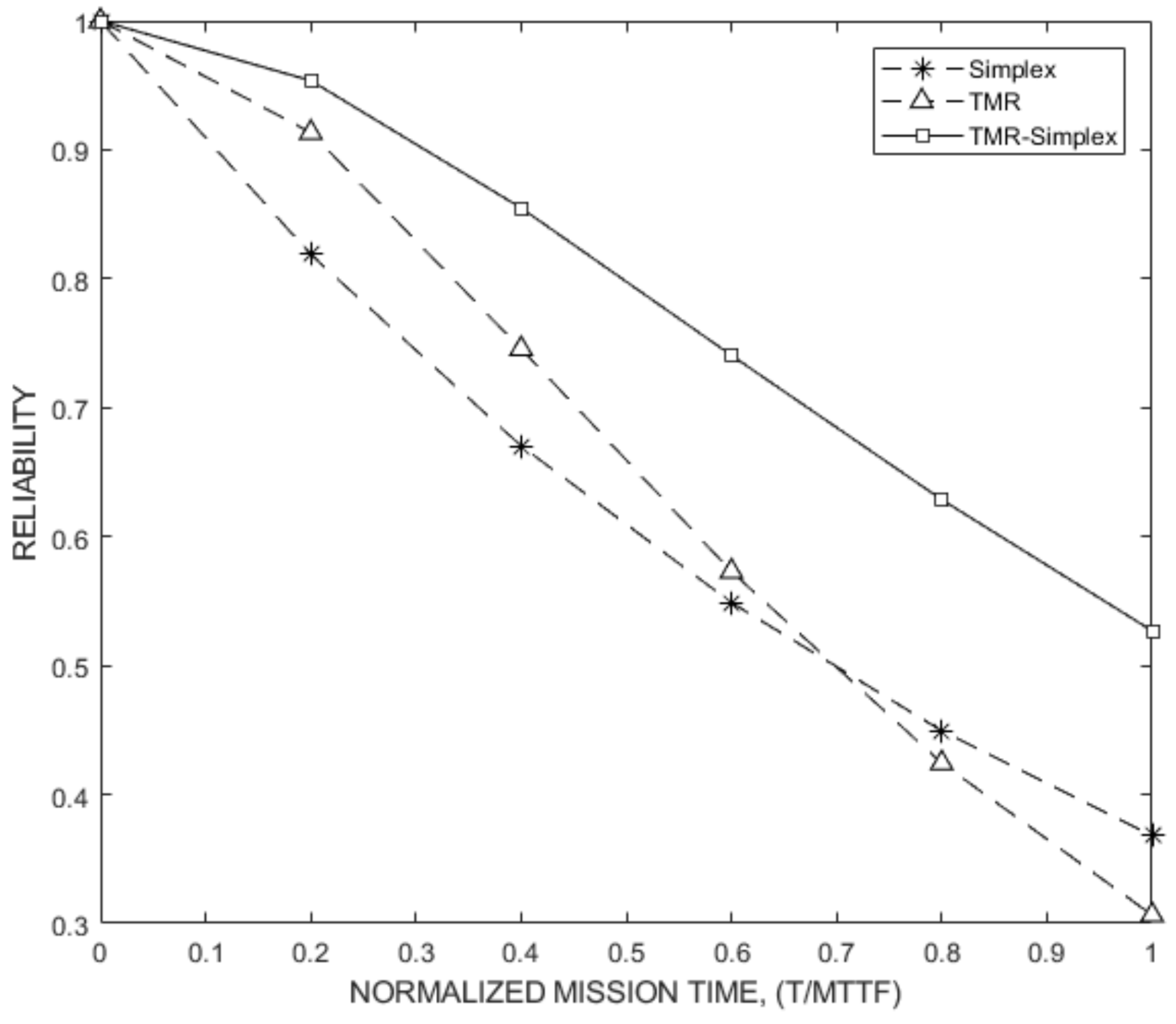
TMR offers significantly better reliability than Simplex (unmitigated system) for short mission times. It is mostly used in applications in which mission times are typically short compared to component life. This is because, after the first failure, TMR is equivalent to a system of two modules in series, with the failure rate double that of a Simplex system. If Rm is the reliability of one of the modules (Simplex system), the reliability equation of the TMR system if an ideal voter is assumed is given by [
21]:
A special form of TMR that combines advantages of TMR and Simplex in one system is TMR/Simplex, which is a reconfigurable, masking redundancy method in which differences in the outputs of the modules are detected and cause a reconfiguration of the TMR system. In particular, it detects a single module failure; the failed module and one of the good modules are discarded leaving one remaining good module. The reliability of the TMR/Simplex system if an ideal voter is assumed is given by [
22]:
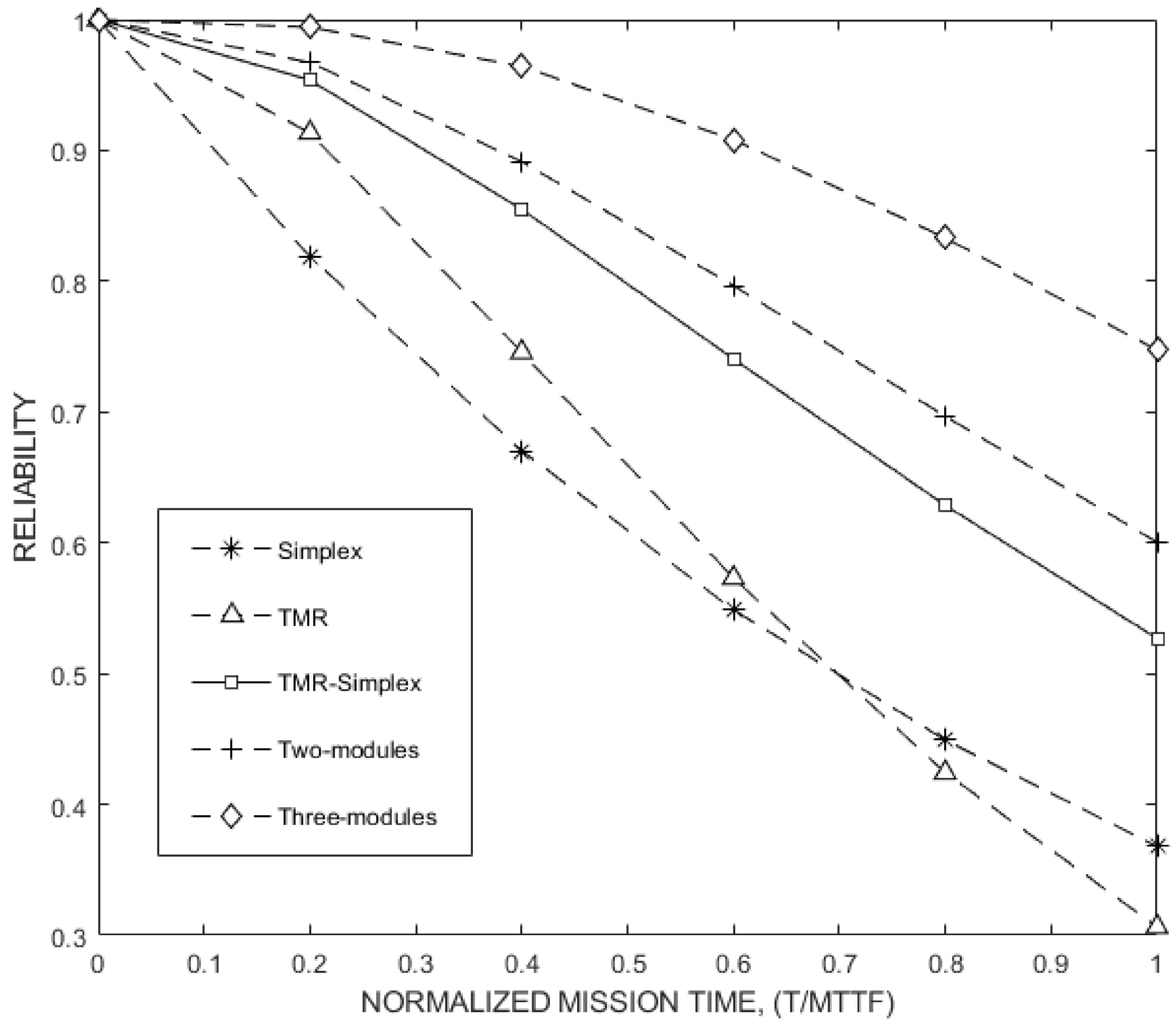
Figure 1 contrasts the reliability of Simplex, TMR, and TMR/Simplex systems versus the normalized mission time (time/MTTFsimplex). As can be seen from
Figure 1, TMR is better than Simplex until 0.7 MTTFsimplex; however, TMR/Simplex is always better than either TMR or Simplex alone.
As a measure of radiation hardness indicator, a parameter that has been found valuable for evaluating reliable systems is the Reliability Improvement Factor (RIF) [
22,
23]. This is defined as the ratio of the probability of failure of the non-redundant system to that of the redundant system. If R
N and R
R are the reliabilities of the non-redundant and the redundant systems, respectively, for a given mission time, and at a given radiation level, then:
Therefore, assuming Simplex module failure rate, λ = 5%, the RIF over the Simplex system of the TMR method is 7.25, whereas the RIF of the TMR/Simplex scheme over the Simplex system is 14.3.
The literature reports the output of research showing alternative methods to TMR or TMR/Simplex, which have better reliability and reduced overhead costs [
24,
25]. However, excluding Lima’s [
26] hybrid method, which has been shown to provide reliability benefits equivalent to those of TMR at a lower cost, no other method has been reported in the literature.
2. The Proposed Technique
The TMR/Simplex scheme provides higher reliability than either the TMR or Simplex system alone, consequently increasing the mission time for which the scheme can be used. However, it abandons a working resource and completely fails as soon as the selected good module fails; thus, another technique is desired that will not discard a working resource or cause a complete system failure as soon as the second module fails. In addition, the scheme would be suitable for a radiation-tolerant digital controller design.
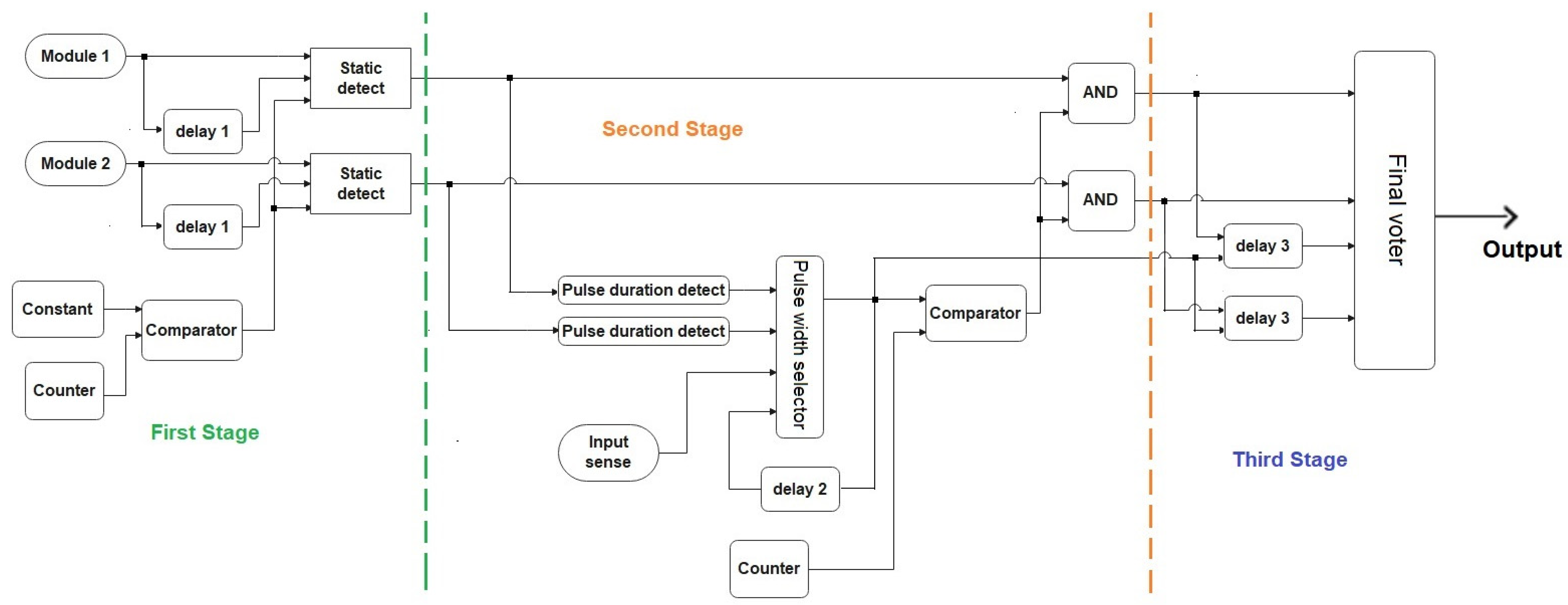
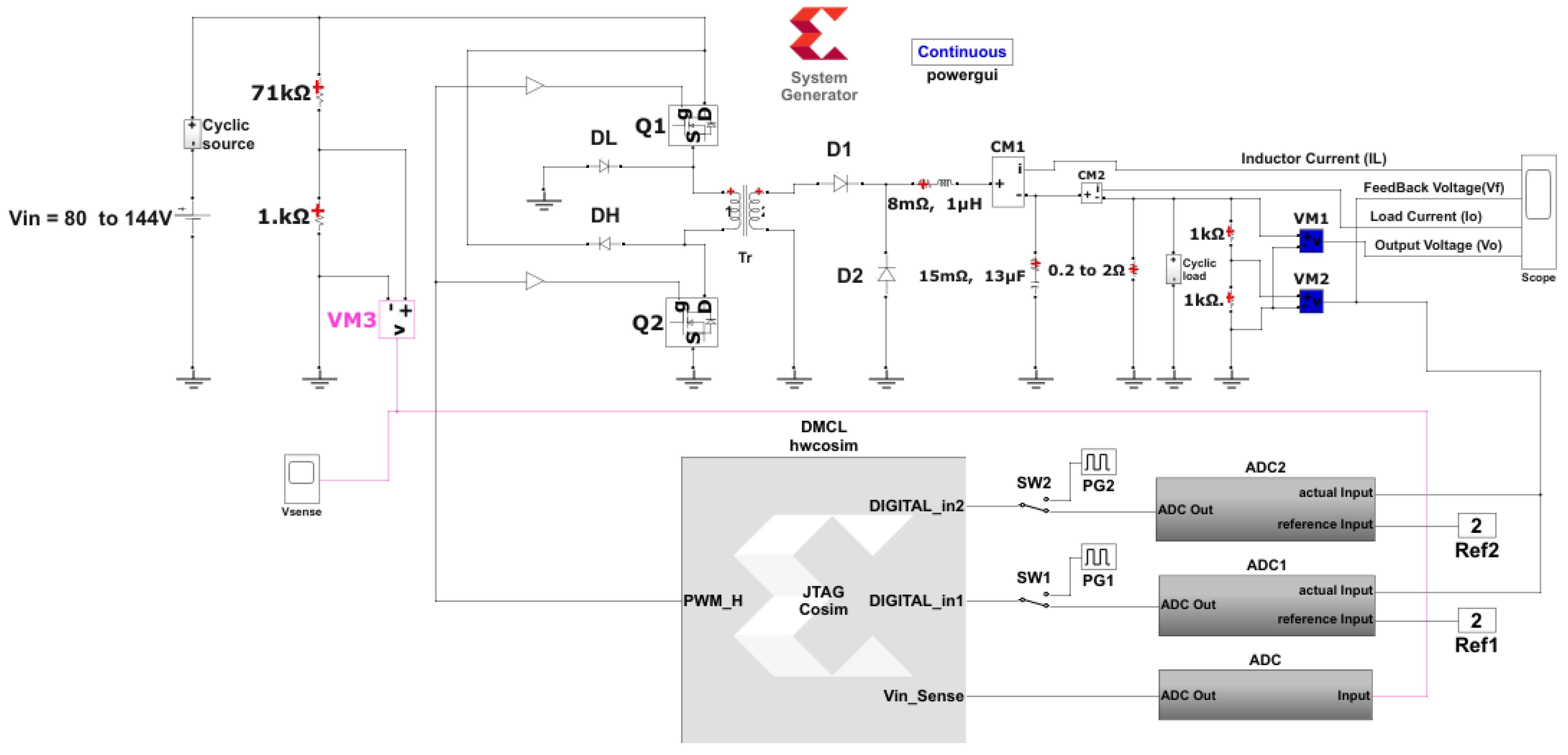
In an effort to address the above research questions, a new redundancy architecture is proposed, as shown in
Figure 2. In this architecture, a hybrid redundancy scheme that combines Spatial and Temporal redundancies is used to design a high-reliability redundancy scheme that mitigates the problems encountered with the ordinary TMR/Simplex technique.
The motivation for the proposed technique rests on the fact that radiation-induced faults result in one or more of the following effects on the DC-DC converter PWM controller output [
27,
28,
29]:
A change in pulse duration(s) of the PWM controller output (for one or more cycles).
A loss of pulse (due to complete failure of the PWM controller; mostly assumed to be due to the permanent change in output to logic-low or 0).
Missing pulses (which occur because the PWM controller’s output is stuck at logic-high or logic-low for one or more cycles).
For a given input voltage, the operating duty cycle and, consequently, the logic-high duration of the pulse generated by the PWM controller can be known. The knowledge of this pulse duration can be used to detect the occurrences of the three radiation-induced fault categories mentioned above and mask them so that their effect does not alter the correct output state.
To illustrate the concept, a two-module implementation of the proposed technique is shown in
Figure 2. However, the numbers of possible paralleled redundant elements are limited only by other constraints, such as space and power requirements of a given design; otherwise, 2, 3, 4, 5, 6, 7, etc., redundant elements, irrespective of being an odd or even number of elements, can be paralleled to reach the required level of reliability. Consequently, for radiation hardening half-duty limited DC-DC converters, the reliability obtained from the proposed technique outweighs most, if not all, of the ordinary modular redundancy techniques.
Figure 2 shows three stages of the proposed voter. The functioning of each stage is as follows:
2.1. First Stage
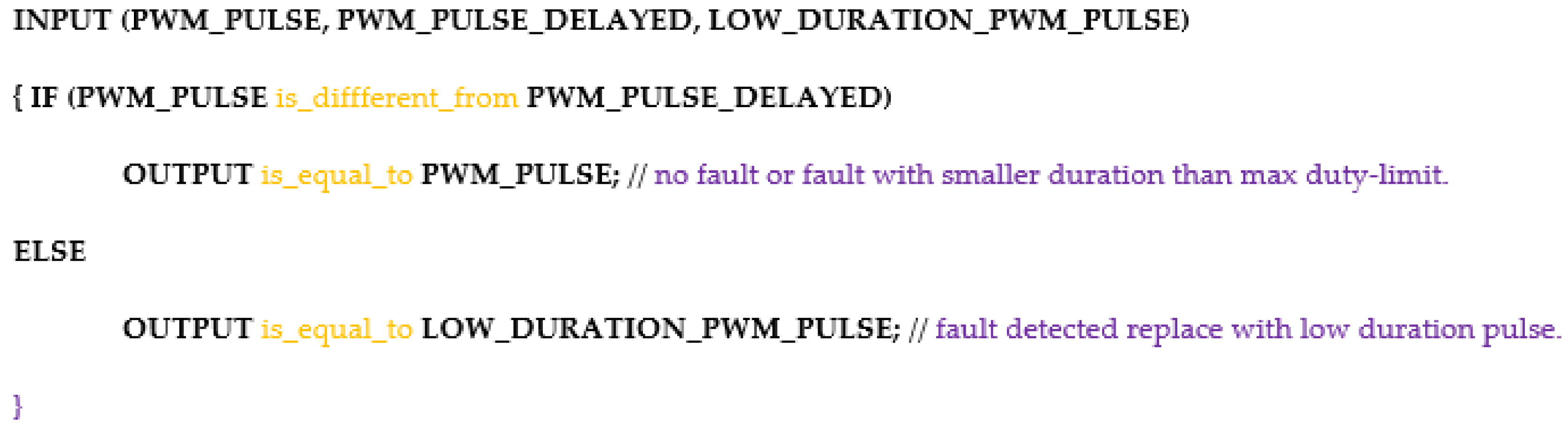
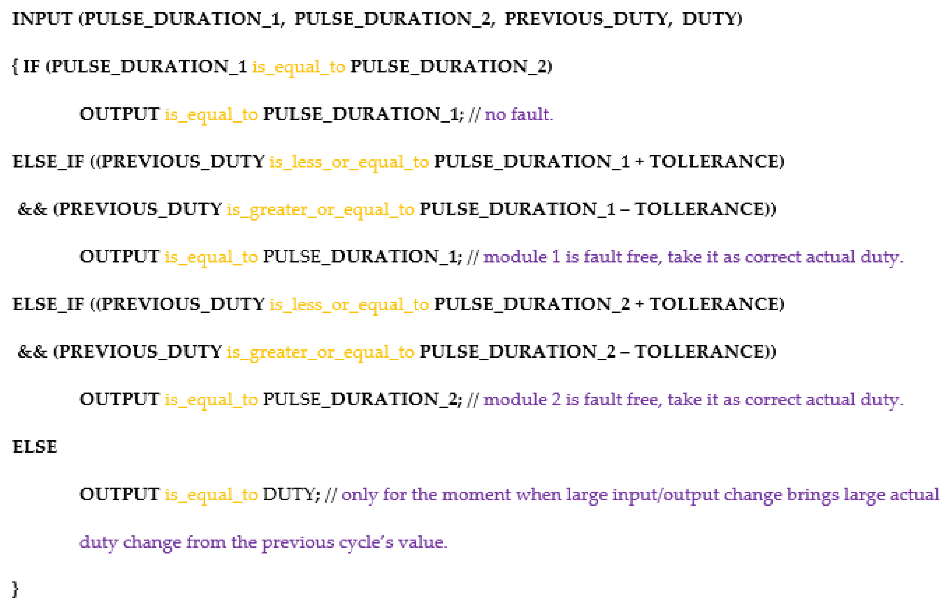
This stage consists of a counter, a comparator, a constant block, two delay blocks, and two first-stage voters. In this stage, the following faults are detected,
If the above two fault categories are detected, these controllers’ outputs are replaced with a low-duration pulse of the same frequency. The actual masking of these fault types happens at the third stage. The first-stage voter (static detect in
Figure 2) inputs the following signals:
Each module’s PWM pulse output;
Each module’s PWM pulse output delayed by the maximum duty-limit used;
A low-duration PWM pulse of the same frequency.
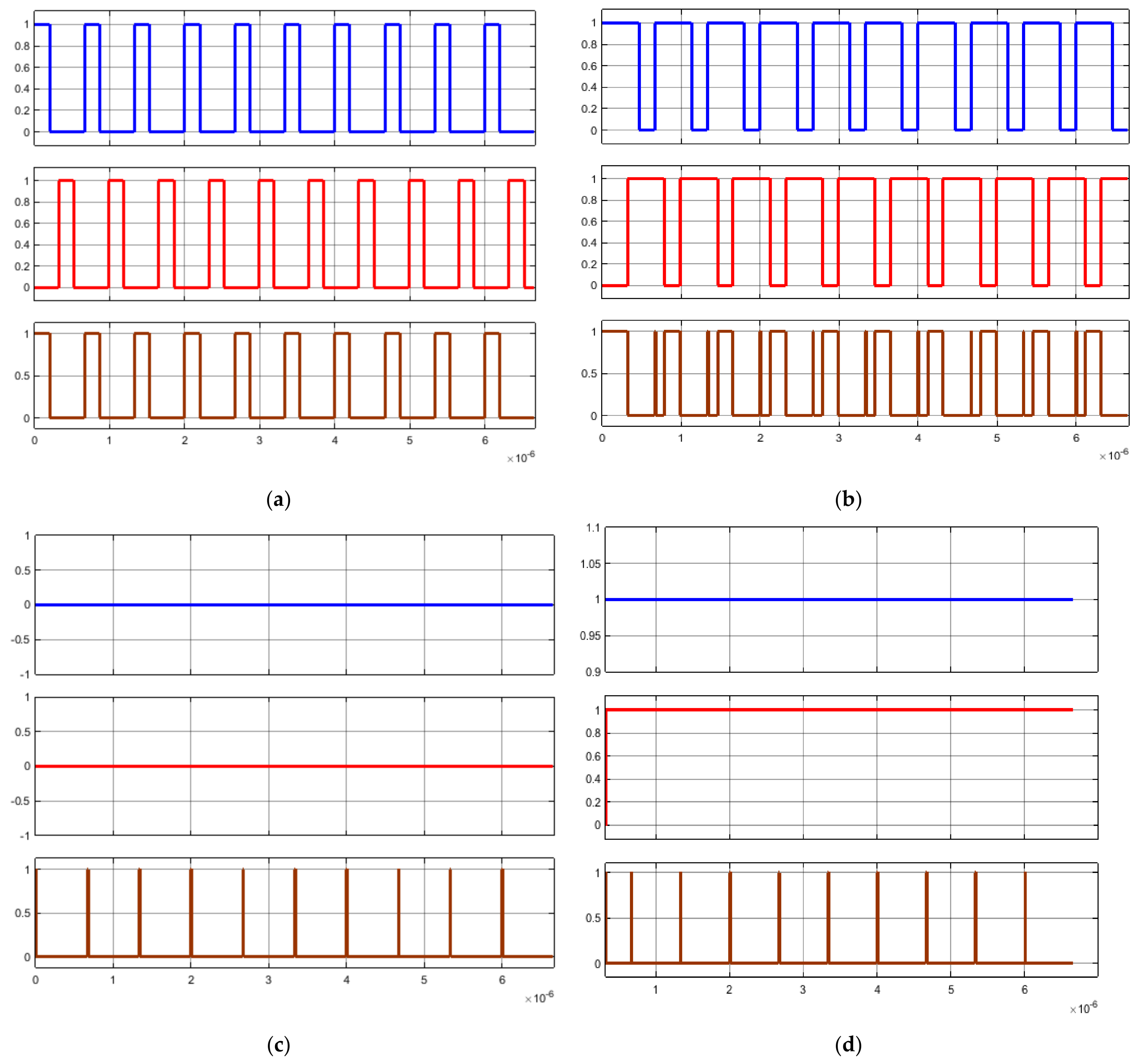
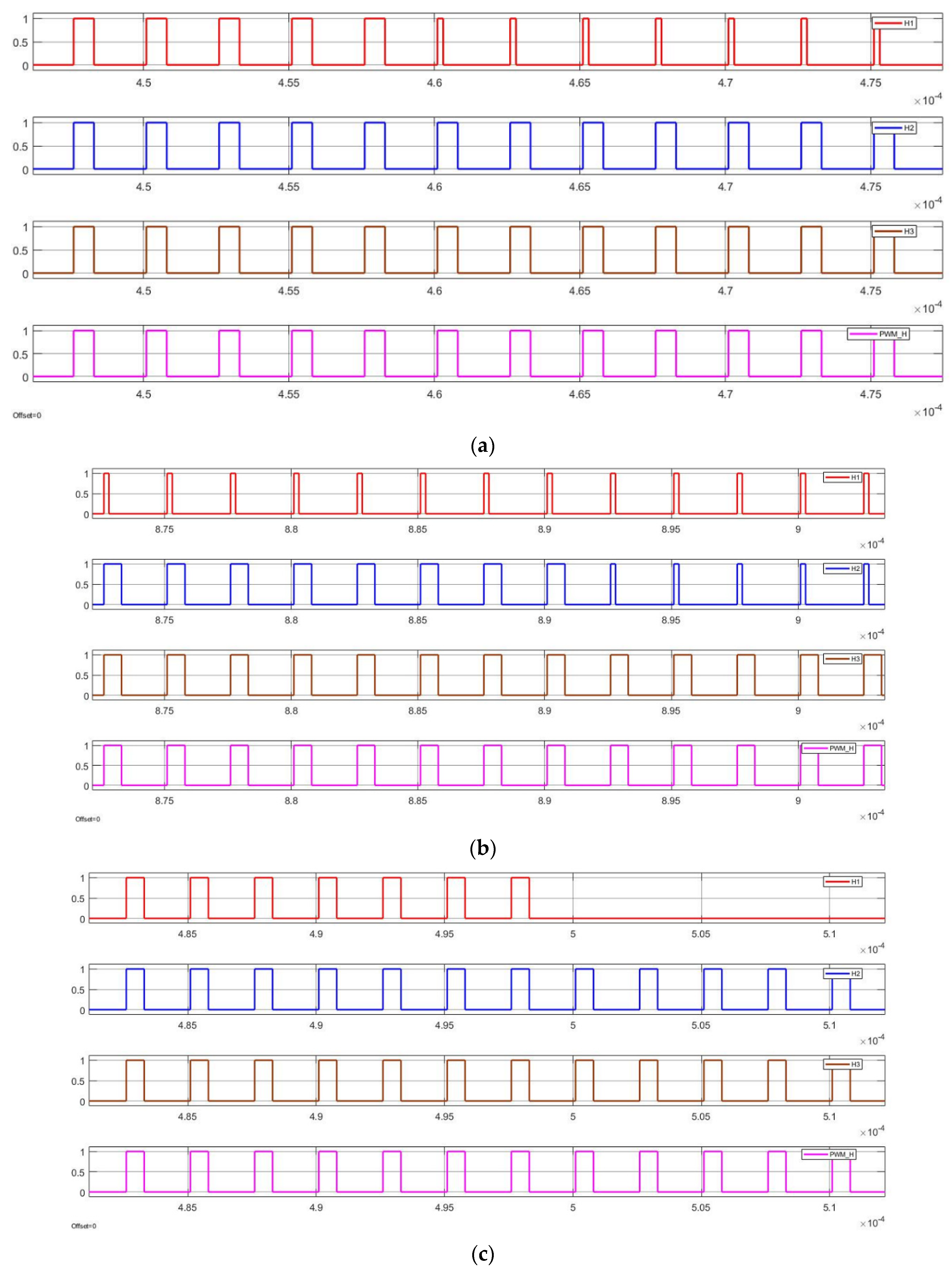
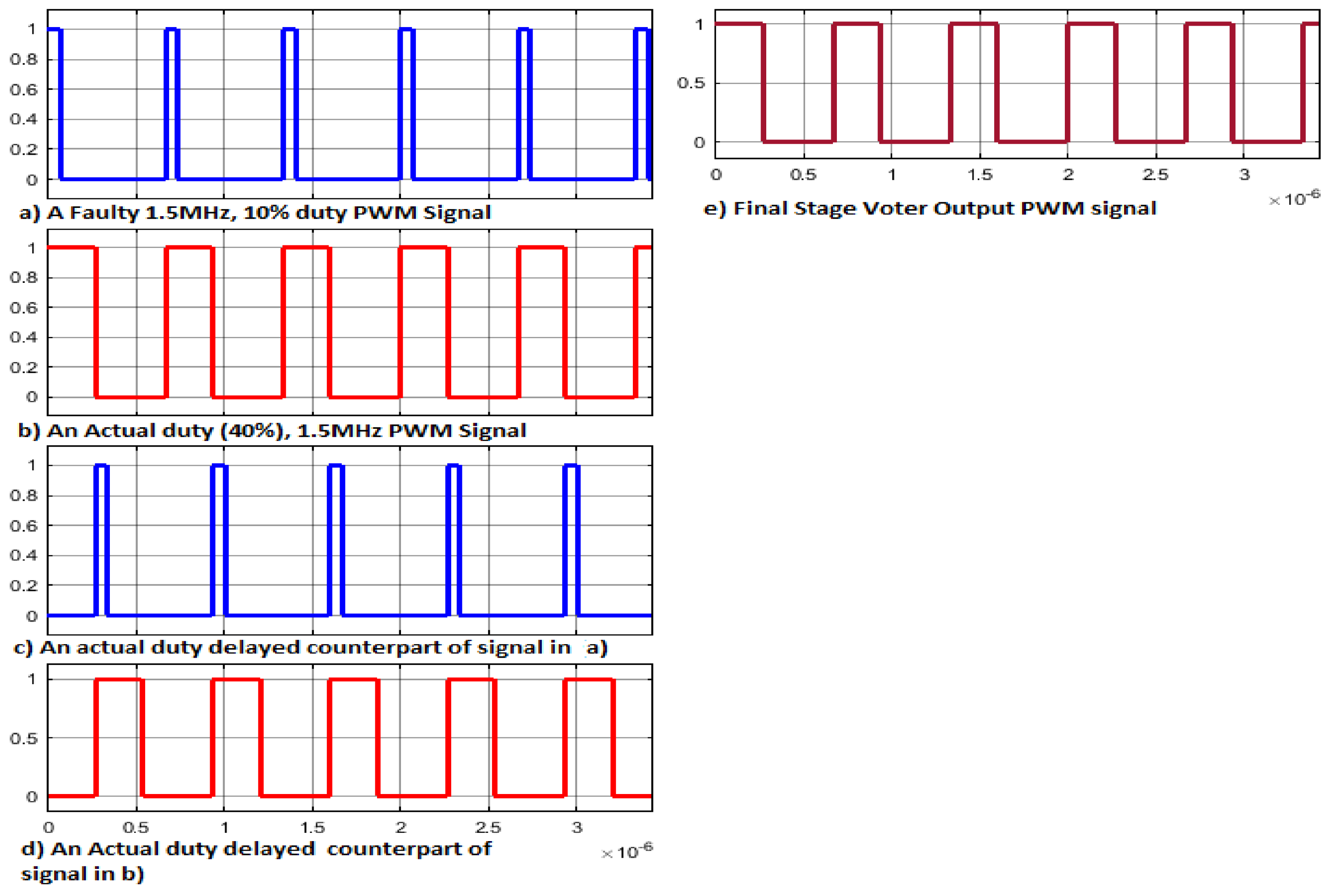
In this stage, if each module’s PWM output pulse is free from the faults categorized above or if radiation causes a pulse-duration change smaller than the fixed maximum duty-limit used, then a comparison of that module’s PWM output pulse and its fixed maximum duty-limit delayed counterpart should result in a difference, as shown in
Figure 3a (upper-blue and middle-red). If so, the first-stage voter propagates that pulse to the next stage as shown in
Figure 3a (lower-brown). However, if radiation causes a change in the pulse-duration larger than the maximum duty-limit used, then the first-stage voter passes that pulse only for the duration of time for which that pulse and its maximum duty delayed counterpart have dissimilarity; otherwise, the low-duration pulse is passed as shown in
Figure 3b. Furthermore, if radiation causes a fault of being permanently or temporarily stuck at logic-low or logic-high, a comparison with its fixed maximum duty-limit delayed equivalent will not result in a difference. In this case, the first-stage voter will replace that particular module’s output with a low-duration pulse with the same frequency, as shown in
Figure 3c,d, respectively. The first-stage voter pseudocode is shown in
Figure 4.
Note that this stage detects either permanent or temporary stuck at logic-low or stuck at logic-high faults that persist for one or more PWM cycles, and faults that result in a change in PWM pulse duration that is larger than the maximum duty-limit used. However, radiation-induced faults that result in a change in PWM pulse duration that is smaller than the maximum duty-limit are not detected in this stage.
2.2. Second Stage
This stage consists of a counter, a comparator, a delay block, two pulse-duration detection algorithm blocks, and two two-input AND blocks. This stage performs the following functions:
Detects the pulse-durations of each inputted pulse and decides the current actual pulse duration.
Detects and rejects faults that result in a PWM pulse duration change smaller than the maximum duty-limit but larger than the actual PWM pulse duration
In this stage, the pulse durations of each inputted pulse are detected, and the actual pulse duration is selected and used to generate a pulse that will be ANDED with the first stage’s outputs. The ANDING process will allow, passing to the third stage, only those PWM pulses that have equal or smaller pulse-durations than that of the selected actual pulse duration.
Note that the previous correct PWM cycle’s duty-value, and the current input voltage value (that is, the fact that the product of the input voltage and primary turn-on time is almost a constant value, no matter how fast the input voltage changes), is used to select the correct pulse duration in the second-stage voter (pulse width selector block in
Figure 2). Therefore, the only faults that can pass through this stage are those that result in smaller pulse durations than that of the actual pulse duration.
The second stage works by inputting:
The outputs from the pulse-duration detectors;
The previous PWM cycle’s duty-value;
The current input voltage–output voltage relation, that is, current duty-value calculated using the equation:
where N is the turn-ratio and NPWM = 2
8 = 256 for the 8-bit DPWM used in the article. Here, because N, NPWM, and output voltage are constants, only the current input voltage value is sensed by the input sensing circuit.
The pseudocode for the second-stage pulse width selector block in
Figure 2 is shown in
Figure 5:
The TOLERANCE value is based on the allowable output voltage variation/tolerance. The value used in the article is 2 clock durations, which corresponds to an allowable duty-value variation of 0.78% or output voltage variation of a maximum of 140 mV above or below the nominal 4 V value (maximum of 140 mV variation occurs at the largest input voltage). The TOLERANCE value can be tightened if required.
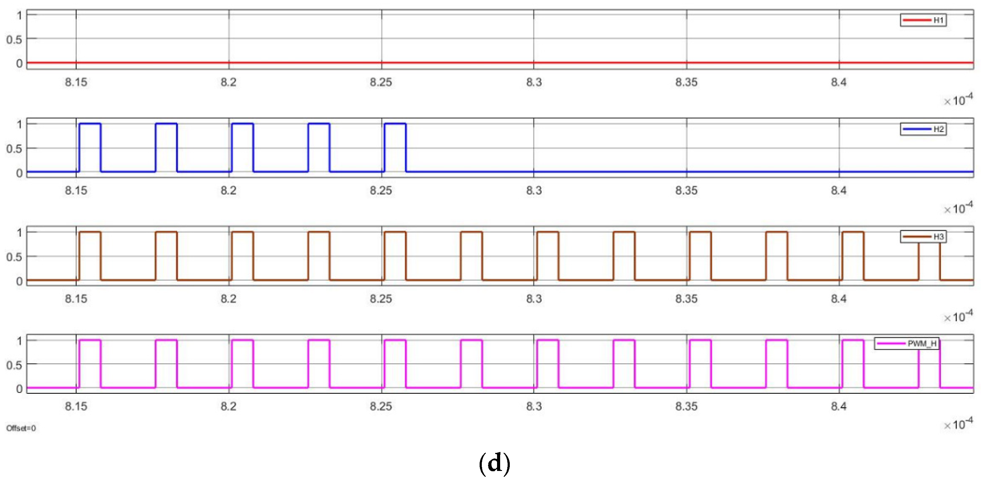
Figure 6 below shows the simulation runs of the three-module implementation of the proposed technique. In the figures, initially the three-module system is running with the actual duty-value of 30%. Then, after approximately 0.46 milliseconds, the first module is switched to a duty-value of 10% to emulate a radiation-induced fault (
Figure 6a); after approximately 0.8925 milliseconds, the second module is switched to a duty-value of 10% (
Figure 6b).
Figure 6c shows outputs after AND blocks with the first module switched to a duty-value of 80% after approximately 0.4975 milliseconds of the simulation run, and
Figure 6d shows the outputs with the second module switched to a duty-value of 80% after approximately 0.8275 milliseconds of the simulation run. In
Figure 6c,d, because faulty pulses that have larger pulse durations than the maximum duty-value are masked by the first stage, the outputs after AND blocks are constant zero-duration pulses which can easily be masked by the third-stage voter. In all figures, the bottom pulse graph shows the resultant actual PWM pulse output after the third stage during the simulation runs. This shows that the failure(s) of one or two module(s) is masked by the two or single fault-free remaining module(s).
2.3. Third Stage
This stage consists of two run-time delay blocks and the final voter. In this stage, a run-time, dynamically generated, delay is used to detect and reject smaller pulse-duration faulty pulses that have passed through the second stage.
The pseudocode for the third stage is similar to that of the first stage, except that in the third stage, no low-duration pulse is required as a replacement for the faulty pulses; in addition, the delay duration is dynamically determined at the second stage and, thus, is not constant. The final voter found in this stage determines the final correct actual PWM pulse by inputting the two redundant modules’ PWM outputs and their actual duty-value delayed counterparts.
The pseudocode for the third stage is shown in
Figure 7:
As can be observed from
Figure 8, although the actual pulse-duration delayed pulse (
Figure 8d) results in a dissimilarity compared to the actual PWM pulse (
Figure 8b), at each clock cycle in the PWM cycle the smaller pulse-duration faulty pulse (
Figure 8a) is not different from its actual pulse-duration delayed equivalent (
Figure 8c), which can easily be detected and rejected by the final voter.
3. Reliability Analysis of the Two-Modules Implementation Case
To conduct an effective evaluation of the dependability of a given fault tolerant system, a measure of reliability is required. Although the true reliability obtained from the proposed technique is dependent on the number of paralleled redundant modules, and increases with the number of modules, the reliability of the two-module implementation case, shown in
Figure 2, can be calculated. Assuming Rm to be the reliability of one of the modules (Simplex system), the reliability expression of the proposed technique, if an ideal voter is assumed, can be derived from the following equations:
Therefore, the RIF of the proposed two-module implementation over the Simplex system is 20.8. This represents a 2.87-fold and 1.46-fold improvement in RIF over the ordinary TMR and TMR/Simplex schemes, respectively, for the same system.
The graph in
Figure 9 compares the reliability of Simplex, TMR, TMR/Simplex, and the proposed technique implementations with two and three modules versus the normalized mission time (time/MTTFsimplex).
As can be seen from
Figure 9, the proposed technique provides the best reliability for all
, compared to either TMR or TMR/Simplex methods, which makes it suitable for applications to relatively longer mission times. The graph also accentuates the claim that the reliability obtained from the proposed technique increases with the increase in the number of paralleled redundant elements.
4. Case Study
The Dual-Switch Forward Converter
Among the different topologies of DC-DC converters, those considered suitable for applications in radiation environments are required to provide insulation between input and output of the converter, and the power switch arrangement should not cause a short circuit at the input of the converter in the case of a fault caused by radiation. Therefore, Forward or Flyback converters are frequently selected [
30].
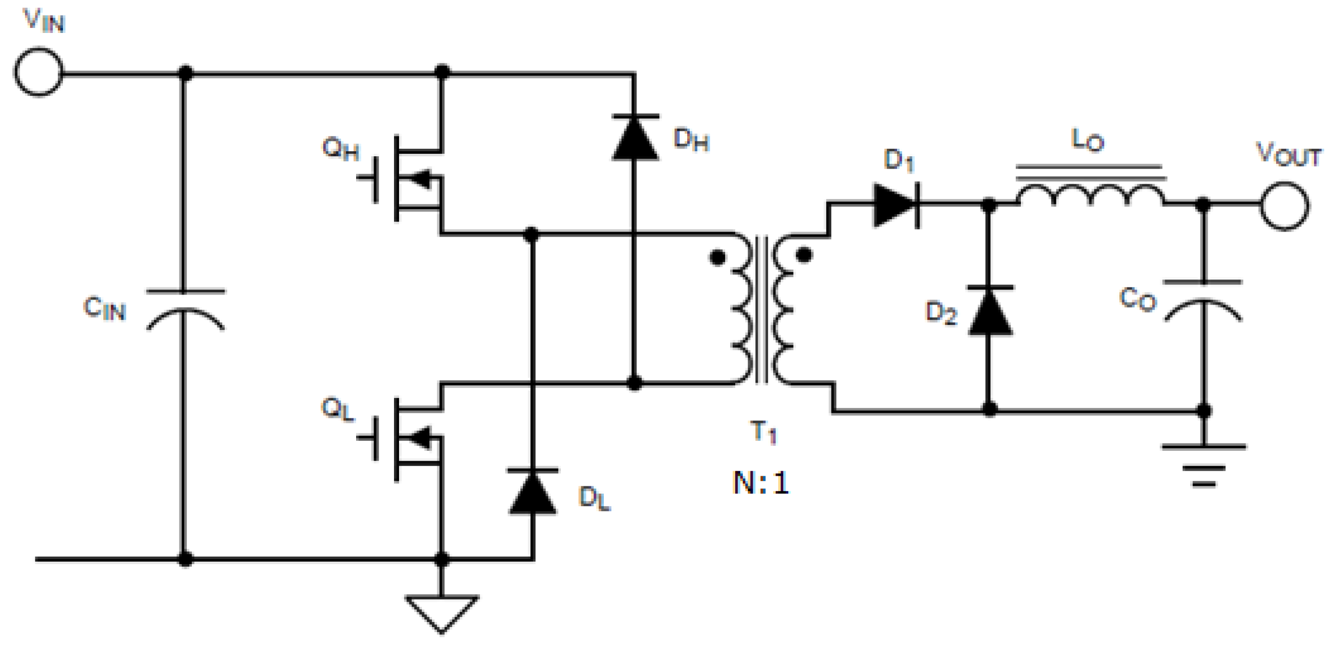
The Dual-Switch Forward converter, like the typical Single-Switch Forward converter, is derived from the Buck converter topology. The key difference between a Forward converter and a Buck converter is that a transformer is introduced in the Forward converter. The transformer creates the input–output separation, and the turn ratio offers a means to adjust the duty cycle for the particular input and output voltage requirements of the application.
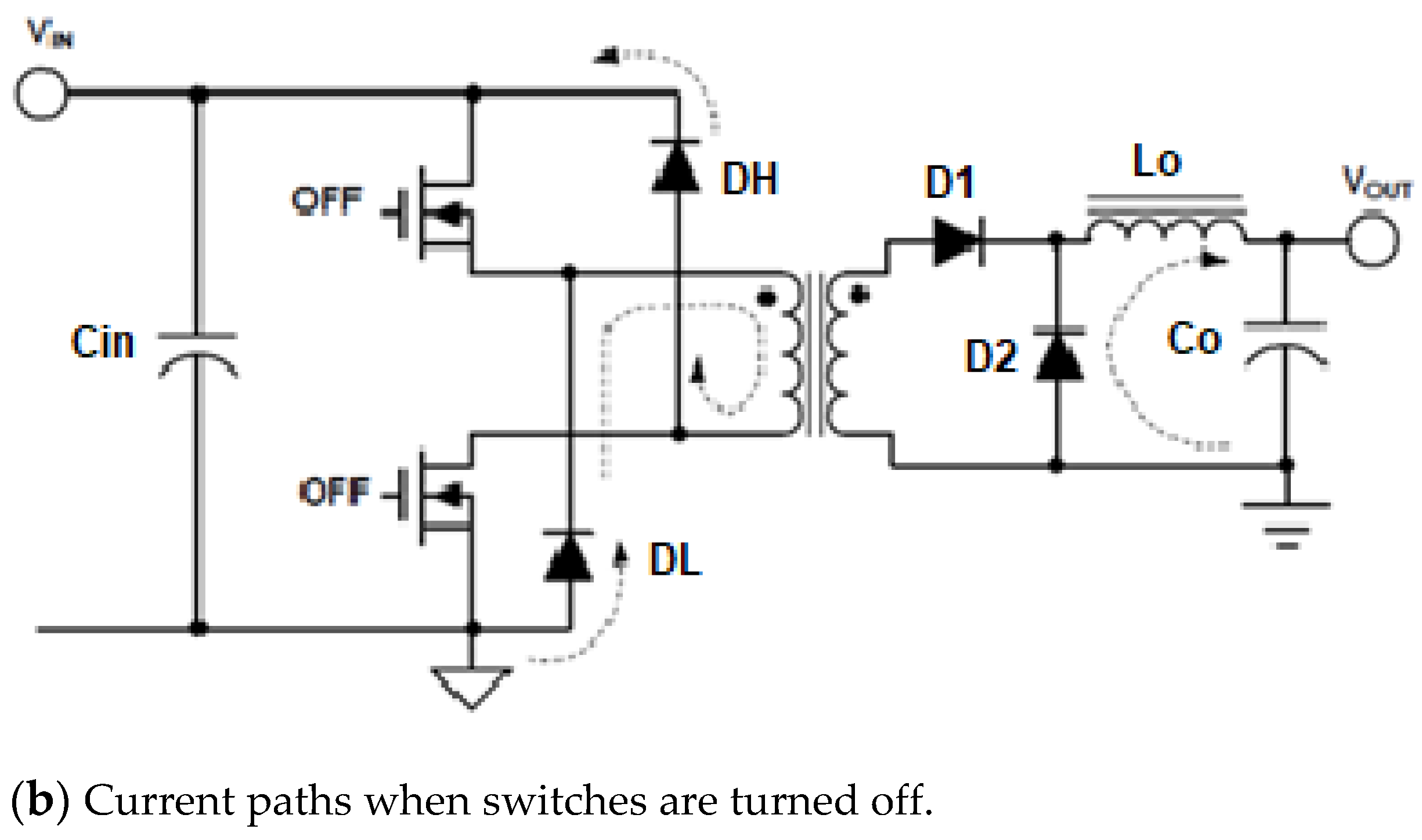
Figure 10 illustrates the Dual-Switch Forward converter topology. The circuit consists of an input capacitor CIN, two switches QH and QL, clamp diodes DH and DL, a power transformer T1, rectifier diodes D1 and D2, an inductor Lo, and a capacitor Co. With a somewhat higher cost, the rectifier diodes D1 and D2 on the secondary side of the power transformer can be replaced with synchronous rectifier switches to improve efficiency in applications with relatively low output voltage.
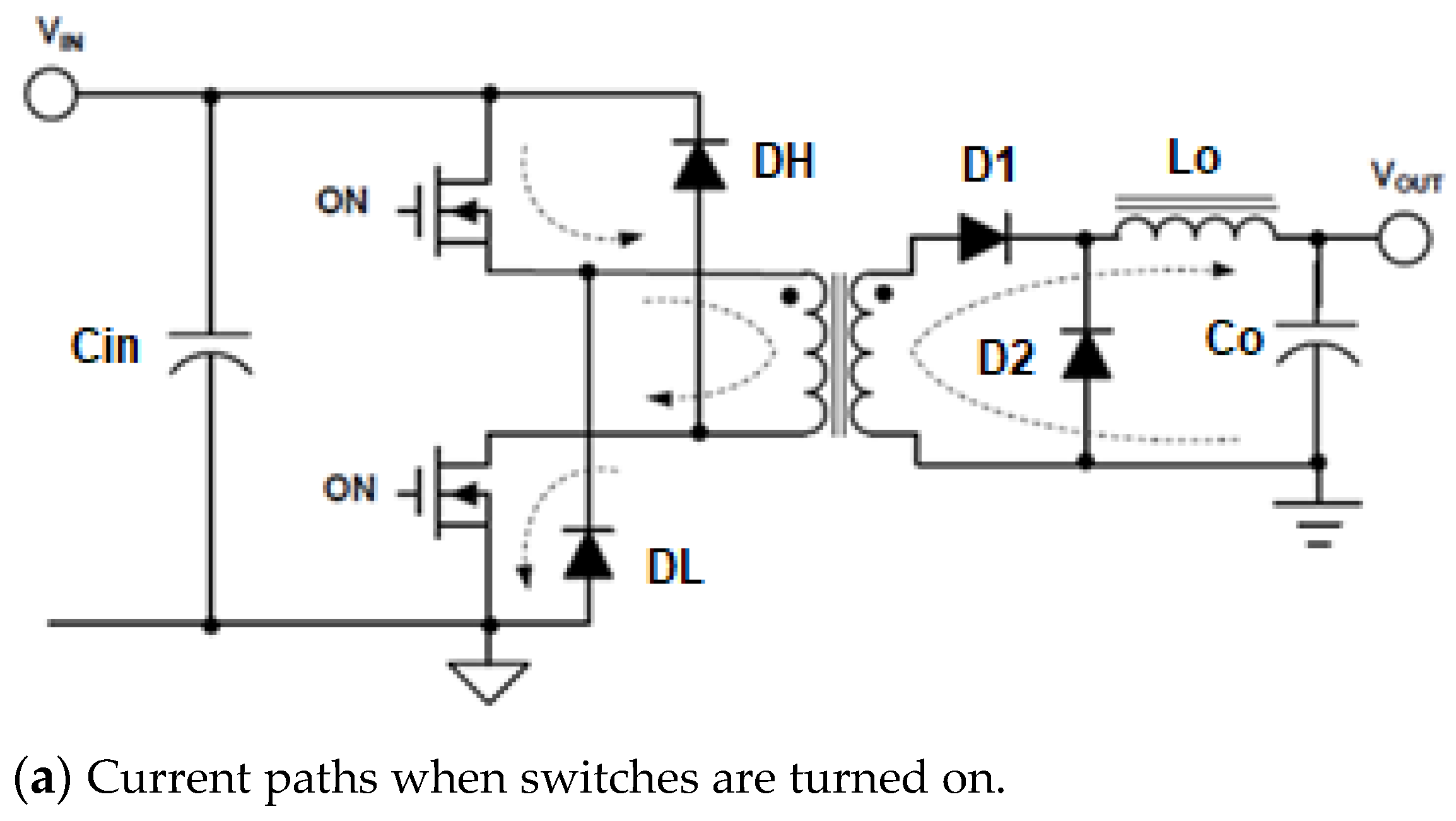
Figure 11 shows the two operational modes of the Dual-Switch Forward converter. During operation, the two switches are turned ON and OFF simultaneously. The output voltage is regulated by modulating the duty cycle of the switches. The relationship between the input voltage VIN, output voltage VOUT, duty cycle D, rectifier diode forward-drop VF, and transformer turns ratio N is defined by the following equation:
When the two switches are turned ON, as shown in
Figure 11a, the input voltage is applied to the primary power transformer. Consequently, the transformer core is magnetized, and the power flows to the secondary side circuit through the transformer coupling. When the two switches are OFF, as shown in
Figure 11b, the flow of power to the primary is cut off. The voltage across the primary winding is reversed due to the residual magnetizing inductance of the transformer, forcing the two clamp diodes DH and DL to conduct. This effectively clamps the switches’ voltage to the input voltage, and applies the input voltage in reversed polarity to the power transformer primary winding to demagnetize and reset the transformer.
The primary of the transformer receives the voltage of the nearly equal magnitude but opposite polarities during the ON and OFF period of the power switches. The maximum duty cycle should be limited to less than 50% to ensure the volt-second balance between the magnetizing and demagnetizing intervals, so that the Dual-Switch Forward converter always achieves a complete reset of the power transformer during each switching cycle.
5. Design Parameters of the Converter
Design specifications of the Dual-Switch Forward converter are shown in the
Table 1 below.
A voltage-mode PWM controller (VMC) for the Dual-Switch Forward converter was designed in the analog domain using the MATLAB control system toolbox. The designed PID compensator has a gain margin of 11.2 dB and a phase margin of 54.2 degrees.
The designed analog compensator was then converted to its equivalent digital form using the bilinear transformation. The final digital PID compensator transfer function is given by:
6. Reliability, Hardware Resources, and Mean-Time-To-Failure (MTTF) Comparisons
The Mean-Time-to-Failure (MTTF) [
21] and reliability comparisons of the methods are shown in
Table 2. As can be seen from
Table 2, the proposed technique is superior for relatively longer mission time applications than either TMR or TMR/Simplex techniques.
Reliability is defined as the probability of not failing in a particular environment for a particular mission time. The MTTF is derivable from the reliability of a given system. The details are given in reference [
21].
Respective MTTF values indicate an average lifespan before the first failure of the system obtainable using each respective technique.
The Reliability Improvement Factor (RIF), also called the Reliability Improvement Index (RII) in some literature, is a measure of the relative advantage of one redundancy technique over the other with respect to the unmitigated system.
Table 3 shows analysis results, for each technique, of hardware resources after synthesis.
7. Testing
To verify the functionality of the proposed technique, the digital controller for the Dual-Switch Forward converter was implemented in the zynq-7000 (zybo) board using a Xilinx system generator and MATLAB/Simulink. The hardware co-simulation block was generated.
A Hardware co-simulation setup was used to emulate radiation-induced faults during simulation. In this setup, the pulse generator block of MATLAB/Simulink was used to emulate (or inject) the pulse-duration changes caused by radiation-induced faults during simulation, and the loss of pulses or stuck at logic-high or stuck at logic-low faults were emulated using a constant block.
Two experiments were designed. Experiment 1 was used to test the injections of the three radiation-induced fault categories in the presence of input disturbances, whereas experiment 2 was used to test the injections of the three fault categories in the presence of output disturbances.
Table 4 shows the duty-value changes injected to emulate the radiation-induced faults, and
Figure 12 shows the synthesizable fault models inserted into the desired places in the VHDL design to emulate the radiation-induced faults.
7.1. Experiment 1
In experiment 1, the simulation interval was initially set at 2 milliseconds, the input DC-bus voltage was made to switch between 144 V and 128 V at a 0.3 millisecond interval, and the output load was fixed at 0.2 Ω. Then the following sequence of events was executed:
The simulation was repeated for all duty-value changes shown in
Table 4 to emulate other fault types.
7.2. Experiment 2
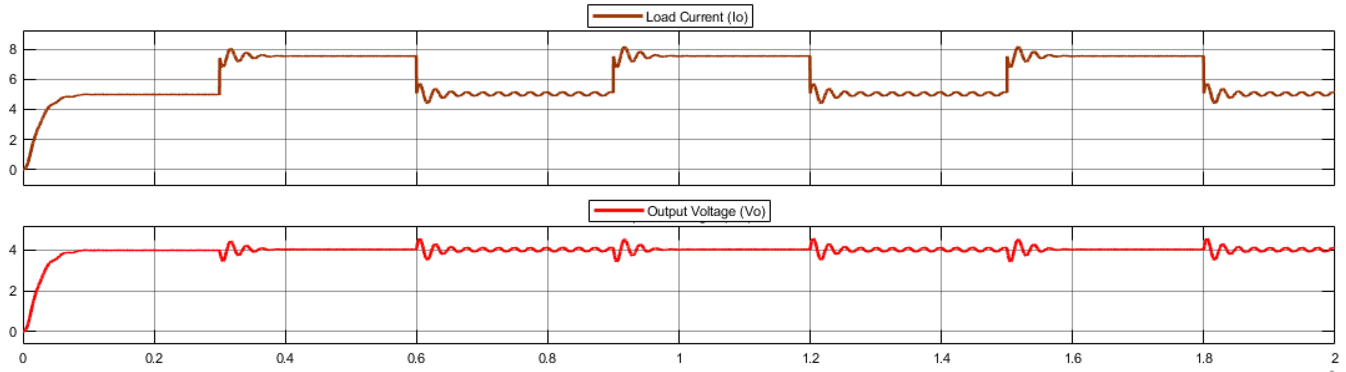
In experiment 2, the same procedure and simulation interval was used as in experiment 1, but the input DC-bus voltage was fixed at 144 V and the output load fixed part was set to 0.8 Ω; in addition, the cyclic load current demand switched between 0 A and 2.5 A so that the total load current demand switched between 5 A and 7.5 A at 0.3 millisecond intervals starting from 0.3 milliseconds after the simulation started.
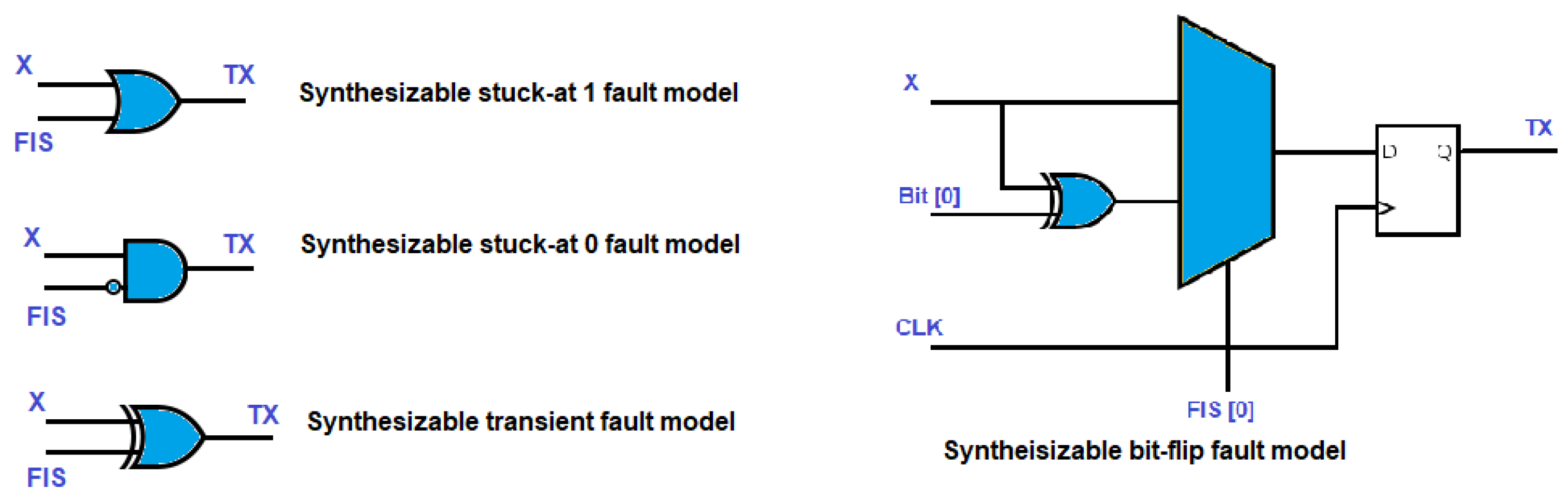
7.3. Testing Using Synthesizable Fault Models
In this case, synthesizable fault models from [
31] were used to inject different fault types into the required places in the VHDL design. The different types of synthesizable faults are shown in
Figure 12.
When injecting the above faults at the required locations in the design, the Fault Injection System (FIS) wire, in
Figure 12, plays a major role. The respective faults would be activated if FIS takes a value of 1, and the faults would become inactive if it takes the value 0.
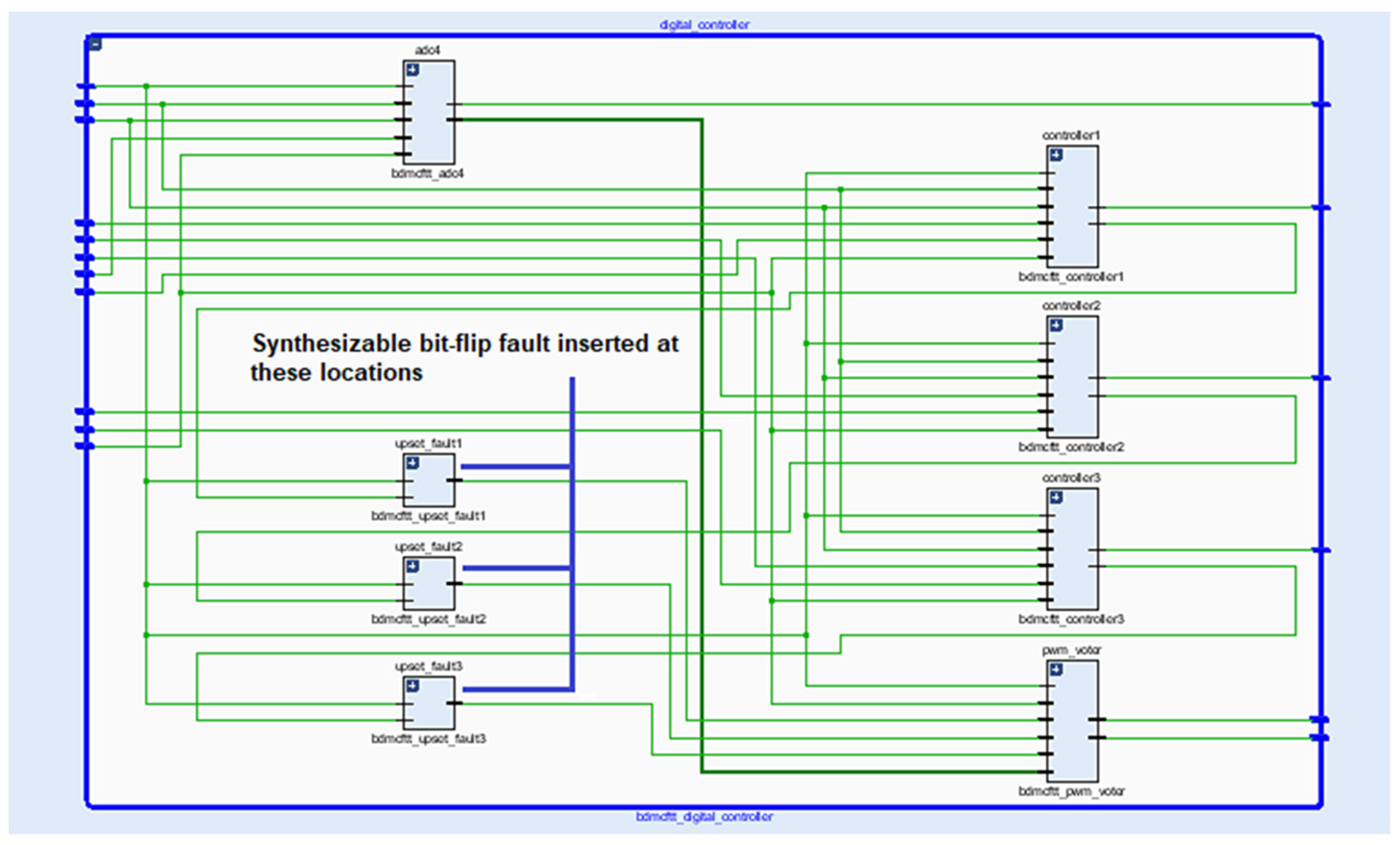
Figure 13 shows the schematic of the system after synthesis with synthesizable bit-flip fault models inserted at the outputs of each controller for a three-module implementation of the technique.
When testing with the synthesizable fault models, similar responses of the converter to those in the cases of experiments 1 and experiment 2 (shown in
Figure 14 and
Figure 15) were observed in the presence of input disturbance (experiment 1) and output disturbance (experiment 2). This proves the effectiveness of the proposed method.
8. Experimental Results
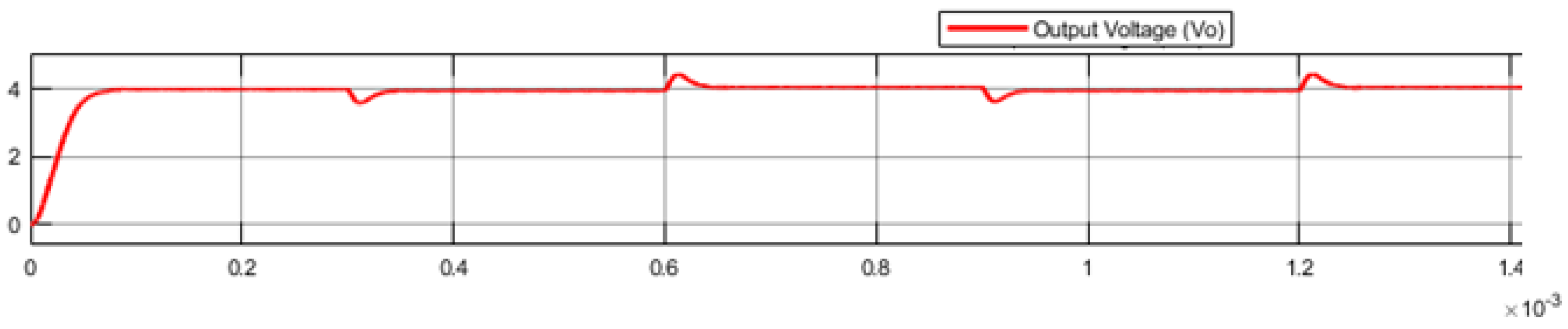
The converter output responses are shown in
Figure 14 for experiment 1, and in
Figure 15 for experiment 2. As can be seen from
Figure 14 and
Figure 15, the converter tolerates the three radiation-induced fault categories previously discussed in the presence of input or output disturbances. Similar converter responses were observed for the different duty-value changes shown in
Table 3, and for the injections of the three radiation-induced fault categories in the presence of input or output disturbances.
Figure 16 shows the hardware co-simulation setup used during the experiments.
9. Discussion
The proposed method is applicable for radiation hardening of half-duty limited DC-DC converters and inverters or similar circuits and/or applications; examples include isolated Dual-Switch Forward and Flyback DC-DC converters. The main limitation is that the method initially adds a delay of two PWM cycles (approximately 1.33 µs in this paper) in the control loop due to the pulse-duration detection algorithms.
The main advantage of the technique is that it can be used to parallel any number of redundant modules, irrespective of being even or odd numbers, with a significant increase in reliability with the number of paralleled redundant modules. Furthermore, the technique continues to function even if only one module is free from radiation-induced faults. The two-module implementation of the technique consumes slightly less resources (LUT) compared to the TMR implementation. Each redundant module’s ADC implementation requires one DSP; thus, TMR uses three DSPs, whereas the proposed method’s two-module and three-module implementations use three and four DSPs, respectively. One more DSP is required for the implementation of the ADC in the input voltage sensing circuit. Overall, the method provides significantly higher reliability, in addition to efficiently using resources. The three-module implementation consumes less than 2% more resources (LUT, registers), and uses one more DSP compared to the TMR, but the increase in reliability is significant.
10. Conclusions
In this paper, a high-reliability hybrid redundancy technique as an alternative to the regular TMR or TMR/Simplex schemes for radiation hardening of half-duty limited DC-DC converters is presented. The technique provides the highest reliability compared to TMR and TMR/Simplex schemes. For the two-module implementation case presented in this paper, the method provides 2.87-fold and 1.46-fold RIF over the Simplex system, compared to TMR and TMR/Simplex techniques, respectively.
The technique can be used to parallel any number of redundant modules, irrespective of being even or odd numbers, with a significant increase in reliability with the number of paralleled redundant modules. The technique can be used for longer mission time applications than both TMR and TMR/Simplex techniques. The technique can be used for half-duty limited DC-DC converters or similar circuits in space systems, and/or in nuclear or high energy physics facilities.
Author Contributions
Conceptualization, S.M.B.; methodology, S.M.B.; software, S.M.B.; validation, S.M.B. and P.L.; formal analysis, S.M.B.; investigation, S.M.B.; resources, S.M.B. and P.L.; writing—original draft preparation, S.M.B.; writing—review and editing, S.M.B. and P.L.; visualization, S.M.B.; supervision, P.L., G.B., V.D.S. and B.K.; project administration, P.L. and S.M.B. All authors have read and agreed to the published version of the manuscript.
Funding
This research was supported by the Home-Grown PhD Program (HGPP) funded by the Ethiopian Ministry of Education.
Conflicts of Interest
The authors declare no conflict of interest.
References
- Pratt, B.; Caffrey, M.; Graham, P.; Morgan, K.; Wirthlin, M. Improving FPGA design robustness with partial TMR. In Proceedings of the 2006 IEEE International Reliability Physics Symposium Proceedings, San Jose, CA, USA, 26–30 March 2006; pp. 226–232. [Google Scholar]
- Bernardi, P.; Reorda, M.S.; Sterpone, L.; Violante, M. On the evaluation of SEU sensitiveness in SRAM-based FPGAs. In Proceedings of the 10th IEEE International On-Line Testing Symposium, Funchal, Portugal, 14 July 2004; pp. 115–120. [Google Scholar]
- Fay, D.; Shye, A.; Bhattacharya, S.; Connors, D.A.; Wichmann, S. An adaptive fault-tolerant memory system for FPGA-based architectures in the space environment. In Proceedings of the Second NASA/ESA Conference on Adaptive Hardware and Systems (AHS 2007), Scotland, UK, 5–8 August 2007; pp. 250–257. [Google Scholar]
- Jacobs, A.; George, A.D.; Cieslewski, G. Reconfigurable fault tolerance: A framework for environmentally adaptive fault mitigation in space. In Proceedings of the 2009 International Conference on Field Programmable Logic and Applications, Prague, Czech Republic, 31 August 2009; pp. 199–204. [Google Scholar]
- Aguiar, Y.Q.; Wrobel, F.; Autran, J.-L.; Leroux, P.; Saigné, F.; Pouget, V.; Touboul, A.D. Design exploration of majority voter architectures based on the signal probability for TMR strategy optimization in space applications. Microelectron. Reliab. 2020, 114, 113877. [Google Scholar] [CrossRef]
- Janson, K.; Treudler, C.J.; Hollstein, T.; Raik, J.; Jenihhin, M.; Fey, G. Software-level tmr approach for on-board data processing in space applications. In Proceedings of the 2018 IEEE 21st International Symposium on Design and Diagnostics of Electronic Circuits & Systems (DDECS), Budapest, Hungary, 25–27 April 2018; pp. 147–152. [Google Scholar]
- Padmanabhan, B.; Mastorakis, N.E. Power, delay and area comparisons of majority voters relevant to TMR architectures. arXiv 2016, arXiv:1603.07964. [Google Scholar]
- Agiakatsikas, D.; Nguyen, N.T.H.; Zhao, Z.; Wu, T.; Cetin, E.; Diessel, O.; Gong, L. Reconfiguration control networks for TMR systems with module-based recovery. In Proceedings of the 2016 IEEE 24th Annual International Symposium on Field-Programmable Custom Computing Machines (FCCM), Washington, DC, USA, 1–3 May 2016; pp. 88–91. [Google Scholar]
- Siddiqui, K.S.; Baig, M.A. FRAM based TMR (triple modular redundancy) for fault tolerance implementation. In Proceedings of the 2011 International Conference on Information and Communication Technologies, Azerbaijan, Baku, 12–14 October 2011; pp. 1–5. [Google Scholar]
- Hudson, S.; Sundar, R.S.S.; Koppu, S. Fault control using triple modular redundancy (TMR). In Progress in Computing, Analytics and Networking; Springer: Singapore, 2018; pp. 471–480. [Google Scholar]
- Lee, G.; Agiakatsikas, D.; Wu, T.; Cetin, E.; Diessel, O. TLegUp: A TMR code generation tool for SRAM-based FPGA applications using HLS. In Proceedings of the 2017 IEEE 25th Annual International Symposium on Field-Programmable Custom Computing Machines (FCCM), Napa, CA, USA, 30 April–2 May 2017; pp. 129–132. [Google Scholar]
- Bernardeschi, C.; Cassano, L.; Domenici, A. SRAM-based FPGA systems for safety-critical applications: A survey on design standards and proposed methodologies. J. Comput. Sci. Technol. 2015, 30, 373–390. [Google Scholar] [CrossRef]
- Li, T.; Liu, H.; Yang, H. Design and characterization of SEU hardened circuits for SRAM-based FPGA. IEEE Trans. Very Large-Scale Integr. (VLSI) Syst. 2019, 27, 1276–1283. [Google Scholar] [CrossRef]
- Tarrillo, J.; Tonfat, J.; Tambara, L.; Kastensmidt, F.L.; Reis, R. Multiple fault injection platform for SRAM-based FPGA based on ground-level radiation experiments. In Proceedings of the 2015 16th Latin-American Test Symposium (LATS), Puerto Vallarta, Mexico, 25–27 March 2015; pp. 1–6. [Google Scholar]
- Schmidt, F.H., Jr. Fault Tolerant Design Implementation on Radiation Hardened by Design SRAM-Based FPGAs. Ph.D. Thesis, Massachusetts Institute of Technology, Cambridge, MA, USA, 2013. [Google Scholar]
- Quinn, H.; Wirthlin, M. Validation techniques for fault emulation of SRAM-based FPGAs. IEEE Trans. Nuclear Sci. 2015, 62, 1487–1500. [Google Scholar] [CrossRef]
- Mousavi, M.; Pourshaghaghi, H.R.; Tahghighi, M.; Jordans, R.; Corporaal, H. A generic methodology to compute design sensitivity to SEU in SRAM-based FPGA. In Proceedings of the 2018 21st Euromicro Conference on Digital System Design (DSD), Prague, Czech Republic, 29–31 August 2018; pp. 221–228. [Google Scholar]
- Giordano, R.; Perrella, S.; Izzo, V.; Milluzzo, G.; Aloisio, A. Redundant-configuration scrubbing of SRAM-based FPGAs. IEEE Trans. Nuclear Sci. 2017, 64, 2497–2504. [Google Scholar] [CrossRef]
- Jung, S.; Choi, J.P. Predicting system failure rates of SRAM-based FPGA on-board processors in space radiation environments. Reliab. Eng. Syst. Saf. 2019, 183, 374–386. [Google Scholar] [CrossRef]
- Steckert, J.; Skoczen, A. Design of FPGA-based radiation tolerant quench detectors for LHC. J. Instrum. 2017, 12, T04005. [Google Scholar] [CrossRef]
- Banteywalu, S.; Khan, B.; De Smedt, V.; Leroux, P. A Novel Modular Radiation Hardening Approach Applied to a Synchronous Buck Converter. Electronics 2019, 8, 513. [Google Scholar] [CrossRef]
- Devries, R.C. Fault-Tolerant Techniques for Radiation Environments. IEEE Trans. Nucl. Sci. 1979, 26, 4320–4326. [Google Scholar] [CrossRef]
- Na, J.; Lee, D. A study on the reliability improvement factor of fault tolerant mechanisms. In Proceedings of the Safe comp 2013 Fast Abstract, Toulouse, France, 24–27 September 2013. [Google Scholar]
- Samudrala, P.K.; Ramos, J.; Katkoori, S. Selective triple modular redundancy for SEU mitigation in FPGAs. Proc. Mil. Aerosp. Appl. Program. Logic Devices (MAPLD) 2003, 344–350. [Google Scholar] [CrossRef]
- Morgan, K.; Caffrey, M.; Graham, P.; Johnson, E.; Pratt, B.; Wirthlin, M. SEU-induced persistent error propagation in FPGAs. IEEE Trans. Nuclear Sci. 2005, 52, 2438–2445. [Google Scholar] [CrossRef]
- de Lima Kastensmidt, F.G.; Neuberger, G.; Hentschke, R.F.; Carro, L.; Reis, R. Designing fault-tolerant techniques for SRAM-based FPGAs. IEEE Design Test Comput. 2004, 21, 552–562. [Google Scholar] [CrossRef]
- Lho, Y.H.; Hwang, Y.S.; Lee, S.Y. A study on radiation effects on PWM-IC controller of DC/DC power buck converter. In Proceedings of the 2013 13th International Conference on Control, Automation and Systems (ICCAS 2013), Gwangju, South Korea, 20–23 October 2013; pp. 1754–1757. [Google Scholar]
- Adell, P.C.; Schrimpf, R.D.; Holman, W.T.; Boch, J.; Stacey, J.; Ribero, P.; Sternberg, A.; Galloway, K.F. Total-dose and single-event effects in DC/DC converter control circuitry. IEEE Trans. Nucl. Sci. 2003, 50, 1867–1872. [Google Scholar] [CrossRef]
- Baronti, F.; Adell, P.C.; Holman, W.T.; Schrimpf, R.D.; Massengill, L.W.; Witulski, A.; Ceschia, M. DC/DC switching power converter with radiation hardened digital control based on SRAM FPGAs. In Proceedings of the Military and Aerospace Programmable Logic Devices (MAPLD) Workshop, San Diego, CA, USA, 19–22 May 2014. [Google Scholar]
- Santos, M.; Ribeiro, H.; Martins, M.; Guilherme, J. Switch mode power supply design constraints for space applications. In Proceedings of the Proc Conf. on Telecommunications–ConfTele, Peniche, Portugal, 9–11 May 2007; pp. 157–160. [Google Scholar]
- Rudrakshi, S.; Midasala, V.; Bhavanam, S.N. Implementation of FPGA based fault injection Tool (FITO) for testing fault tolerant designs. Int. J. Eng. Technol. 2012, 4, 522. [Google Scholar] [CrossRef]
Figure 1.
Reliability versus normalized mission time for Simplex, TMR, and TMR/Simplex systems.
Figure 1.
Reliability versus normalized mission time for Simplex, TMR, and TMR/Simplex systems.
Figure 2.
Implementation of the proposed technique for the two-module case.
Figure 2.
Implementation of the proposed technique for the two-module case.
Figure 3.
First-stage detection process: (a) A 1.5 MHz 30% actual duty PWM pulse (upper-blue), its 48% pulse-duration delayed counterpart (middle-red) and resultant first-stage voter output PWM pulse (lower-brown); (b) a faulty 1.5 MHz 70% duty (larger than the maximum duty, max-duty = 48%), PWM pulse (upper-blue), its 48% pulse-duration delayed counterpart (middle-red) and resultant first-stage voter output PWM pulse (lower-brown); (c) a faulty 1.5 MHz 0% duty (stuck at logic-low fault), PWM pulse (upper-blue), its 48% pulse-duration delayed counterpart (middle-red) and resultant first-stage voter output PWM pulse (lower-brown); (d) a faulty 1.5 MHz 100% duty (stuck at logic-high fault), PWM pulse (upper-blue), its 48% pulse-duration delayed counterpart (middle-red) and resultant first-stage voter output PWM pulse (lower-brown).
Figure 4.
First-stage static detect block pseudocode.
Figure 4.
First-stage static detect block pseudocode.
Figure 5.
Second-stage pulse width selector block pseudocode.
Figure 5.
Second-stage pulse width selector block pseudocode.
Figure 6.
(a) Outputs after AND blocks and the final voter when module 1 is forced to output 10% duty to emulate a sudden change in pulse duration. (b) Outputs after AND blocks and the final voter when module 2 is also forced to output 10% duty to emulate a sudden change in pulse duration. (c) Outputs after AND blocks and the final voter when module 1 is forced to output 80% duty to emulate a sudden change in pulse duration. (d) Outputs after AND blocks and the final voter when module 2 is also forced to output 80% duty to emulate a sudden change in pulse duration.
Figure 7.
Third-stage final voter block pseudocode.
Figure 7.
Third-stage final voter block pseudocode.
Figure 8.
Third-stage detection and rejection process.
Figure 8.
Third-stage detection and rejection process.
Figure 9.
Reliability versus normalized mission time for Simplex, TMR, TMR/Simplex, and the proposed method for two- and three-module cases.
Figure 9.
Reliability versus normalized mission time for Simplex, TMR, TMR/Simplex, and the proposed method for two- and three-module cases.
Figure 10.
Dual-Switch Forward converter topology.
Figure 10.
Dual-Switch Forward converter topology.
Figure 11.
Operating modes of Dual-Switch Forward converter.
Figure 11.
Operating modes of Dual-Switch Forward converter.
Figure 12.
Synthesizable fault models.
Figure 12.
Synthesizable fault models.
Figure 13.
Schematic after synthesis showing the location of the insertion of bit-flip synthesizable fault models.
Figure 13.
Schematic after synthesis showing the location of the insertion of bit-flip synthesizable fault models.
Figure 14.
Converter output voltage response during input disturbances in the presence of radiation fault injection (experiment 1).
Figure 14.
Converter output voltage response during input disturbances in the presence of radiation fault injection (experiment 1).
Figure 15.
Converter output voltage and current responses during load disturbances in the presence of radiation fault injection (experiment 2).
Figure 15.
Converter output voltage and current responses during load disturbances in the presence of radiation fault injection (experiment 2).
Figure 16.
Hardware co-simulation setup.
Figure 16.
Hardware co-simulation setup.
Table 1.
Design parameters of the Dual-Switch Forward converter.
Table 1.
Design parameters of the Dual-Switch Forward converter.
| Parameter | Rating Value |
|---|
| DC Input Voltage (Vin) range | 80–144 V |
| Turn ratio, N | 8 |
| Output Voltage (Vout) | 4 V |
| Output Current (Io) range | 2–20 A |
| Inductor (L), ESL | 1 µH, 8 mΩ |
| Capacitor (C), ESR | 13 µF, 15 mΩ |
| Load (R) range | 0.2–2 Ω |
| Switching Frequency (Fsw) | 1.5 MHz |
| Output Power (Po) | 80 Watts |
| Maximum duty cycle (Dmax) | 0.48 |
| Efficiency (η) | >90% |
Table 2.
Reliability and MTTF comparison.
Table 2.
Reliability and MTTF comparison.
| Methods | |
|---|
MTTF
(in years) | Reliability for Mission Time t |
|---|
| t = 1 year | RIF |
|---|
| Simplex | 20 | 0.95 | 1 |
| TMR | 145 | 0.9931 | 7.25 |
| TMR/Simplex | 286 | 0.9965 | 14.30 |
| Proposed Technique (Two Modules) | 417 | 0.9976 | 20.83 |
| Proposed Technique (Three Modules) | 10,000 | 0.9999 | 500 |
Table 3.
Hardware resource comparisons.
Table 3.
Hardware resource comparisons.
| - | DSP
(80) | LUT
(17,600) | Registers
(35,200) |
|---|
| TMR\TMR/Simplex | 3 | 1500 | 1467 |
| Proposed Technique (Two Modules) | 3 | 1317 | 1536 |
| Proposed Technique (Three Modules) | 4 | 1793 | 2094 |
Table 4.
Duty-value change used for different experiment sequences.
Table 4.
Duty-value change used for different experiment sequences.
| Fault Type | Stuck at Logic-Low or Permanent Failure | Duty-Value Changes | Stuck at Logic-High |
|---|
| Sequence No | 1 | 2 | 3 | 4 | 5 | 6 | 7 |
| Duty-Value (%) | 0 | 10 | 40 | 60 | 80 | 90 | 100 |
| Publisher’s Note: MDPI stays neutral with regard to jurisdictional claims in published maps and institutional affiliations. |
© 2021 by the authors. Licensee MDPI, Basel, Switzerland. This article is an open access article distributed under the terms and conditions of the Creative Commons Attribution (CC BY) license (https://creativecommons.org/licenses/by/4.0/).


 ,
, 


