Abstract
The capability of multiple valued logic (MVL) circuits to achieve higher storage density when compared to that of existing binary circuits is highly impressive. Recently, MVL circuits have attracted significant attention for the design of digital systems. Carbon nanotube field effect transistors (CNTFETs) have shown great promise for design of MVL based circuits, due to the fact that the scalable threshold voltage of CNTFETs can be utilized easily for the multiple voltage designs. In addition, resistive random access memory (RRAM) is also a feasible option for the design of MVL circuits, owing to its multilevel cell capability that enables the storage of multiple resistance states within a single cell. In this manuscript, a design approach for ternary combinational logic circuits while using CNTFETs and RRAM is presented. The designs of ternary half adder, ternary half subtractor, ternary full adder, and ternary full subtractor are evaluated while using Synopsis HSPICE simulation software with standard 32 nm CNTFET technology under different operating conditions, including different supply voltages, output load variation, and different operating temperatures. Finally, the proposed designs are compared with the state-of-the-art ternary designs. Based on the obtained simulation results, the proposed designs show a significant reduction in the transistor count, decreased cell area, and lower power consumption. In addition, due to the participation of RRAM, the proposed designs have advantages in terms of non-volatility.
1. Introduction
Binary circuits for long been associated with the design of digital systems for performing computations on two possible logic values (0 or true and 1 or false) in the Boolean space. However, the binary integrated circuit design suffers from various critical issues such as complexity of the interconnects and the pin-out problems which limit the connections inside and outside of the circuit. Interconnects are the main source of power dissipation within a VLSI chip and they comprises 70% of total on-chip capacitance [1]. In integrated circuits, these interconnects occupy additional area, thereby causing several signal integrity issues such as noise and delay jitters. The implementation of energy efficient digital designs becomes quite challenging when scaling down the feature size into a nano-meter regime, owing to reliability and performance issues. Moreover, many real-life applications, such as robotics and process control, face difficulties for systematic implementation only with the conventional binary logic [2]. To get over the limitations of binary logic, a logic system having more than two values that are associated with the logic levels, which is commonly referred to as the multiple valued logic (MVL), can be used for implementing digital system design. MVL is a very effective and practical means to resolve the issues of interconnects in modern circuits. Owing to the fact that the MVL utilizes more than two logic levels, MVL-based systems provide the transmission of a greater amount of information when compared to binary logic systems over a single wire, which helps to significantly reduce the on-chip and off-chip interconnections. The designs utilizing MVL for its implementation offer advantages in terms of increased information density, reduced chip area, and improved computational capability of the integrated circuits. Therefore, the use of MVL designs helps to reduce the circuit complexity and improve energy efficiency in digital system design due to reduced circuit overhead [3]. MVL is one of the new approaches, which increases the radix for computation to lower the complexity of the circuit. The main purpose of using MVL over binary logic is to: (i) reduce the chip area by the transmission of more information through each wire as compared to binary; (ii) increase the speed of information transmission as the information per unit time is increased; and, (iii) reduce the circuit complexity as each MVL element processes more information when compared to the binary element. The introduction of additional levels to the existing binary logic results in MVL systems, with typical examples being that of the ternary and quaternary logic systems [4]. Ternary logic is of considerable interest, due to its ease of implementation and energy efficiency because of the reduced complexity of interconnects and chip area [5]. In addition, ternary circuits can also help to reduce the problems of pin-out and increase in interconnection density in the VLSI systems.
MVL designs can replace the existing binary technologies due to its numerous advantages, but this is highly dependent on the circuit realization techniques that we employ for the implementation of MVL systems. A number of approaches to build MVL based circuit using CMOS or to combine binary and multi-valued blocks in logic circuits has been shown [6]. With the progress of nanotechnology, molecular devices are becoming promising alternatives to the traditional silicon-based CMOS technology [7]. The most promising alternative to silicon transistor for achieving low power and high performance is the Carbon nanotube field effect transistor (CNTFET) [8,9,10]. Carbon Nano Tubes (CNTs) have recently gained significant interest, primarily due to their relatively small dimensions and potential of implementation in many existing as well as emerging technologies. CNTFET could be the most suitable option for replacing conventional MOSFET based on silicon technology, because of its similarities in terms of various characteristics, such as near-ballistic transport operation due to its unique one-dimensional (1D) band structure, which gives the device an excellent driving capability and less power dissipation [11]. The threshold voltage of CNTFET can be controlled by varying the CNT diameter, which is very effective in the design of MVL based circuits. Additionally, CNTFETs (both p-type and n-type) have similar mobility values, which is quite significant for device sizing in complex circuits. However, CNTFETs face some critical challenges in terms of chirality control, fabrication process, growth, and the positioning of single-wall CNTs.
Ternary systems can also be implemented while using another suitable emerging technology, commonly referred to as the Resistive Random Access Memory (RRAM). This is attributed to the fact that the RRAM device can effectively implement multiple logic values (two or more) without the need for extra hardware for the realization of digital designs. Thus, the implementation of ternary logic while utilizing RRAM, provides a unique opportunity for enhanced and novel functionality. The circuit schematic of RRAM is quite simple, having a two terminal metal-insulator-metal (MIM) structure, with the external voltage pulse causing a resistance change within the device [12,13]. Its physical mechanism relies on the formation and annihilation of a conductive filament (CF) in the oxide (dielectric) connecting the two metal electrodes [14,15]. This resistance shift between the high resistance state (HRS) and low resistance state (LRS) is effectively used for data storage in the form of “0” and “1” [16,17,18], respectively. Because of the various attractive features of RRAM, such as higher on/off ratio, non-volatility, good scalability, and low ON-state resistance [19,20], it is employed for configuring logic gates, including the field-programmable gate arrays [21] that are used in the design of digital systems. The RRAM is chosen as the candidate device here, as it has a simple structure, enables high integration density, and it can exhibit switching in the low-power regime [22]. Although making use of RRAM for implementing ternary logic systems is still in its emerging phase, various methodologies for the implementation of binary logic gates with RRAM have already been proposed [23].
The main aim of this paper is to utilize CNTFET-RRAM ternary logic gates for the design of ternary arithmetic circuits in order to explore the advantages in terms of reduction of gate count by utilizing the negation of literals technique. In this manuscript, CNTFET-RRAM ternary combinational logic circuits are proposed and the simulation results while using the HSPICE simulator demonstrates advantages in terms of power consumption and component count when compared to the multi-valued logic designs existing in the literature. Logic states can also be stored in the RRAM due to the addition of RRAM as circuit element. This will ensure the integration of logic computation and data storage into the proposed designs, which opens a new domain of opportunities for exploring intelligent computation systems.
The rest of the paper is presented, as below. Section 2 provides a brief introduction of the carbon nanotube transistors. In Section 3, an overview of ternary logic is presented and the design methodology for various ternary combinational logic circuits is detailed. The simulation results that were obtained from HSPICE software and the comparative analysis are described in Section 4. Finally, Section 5 concludes the paper.
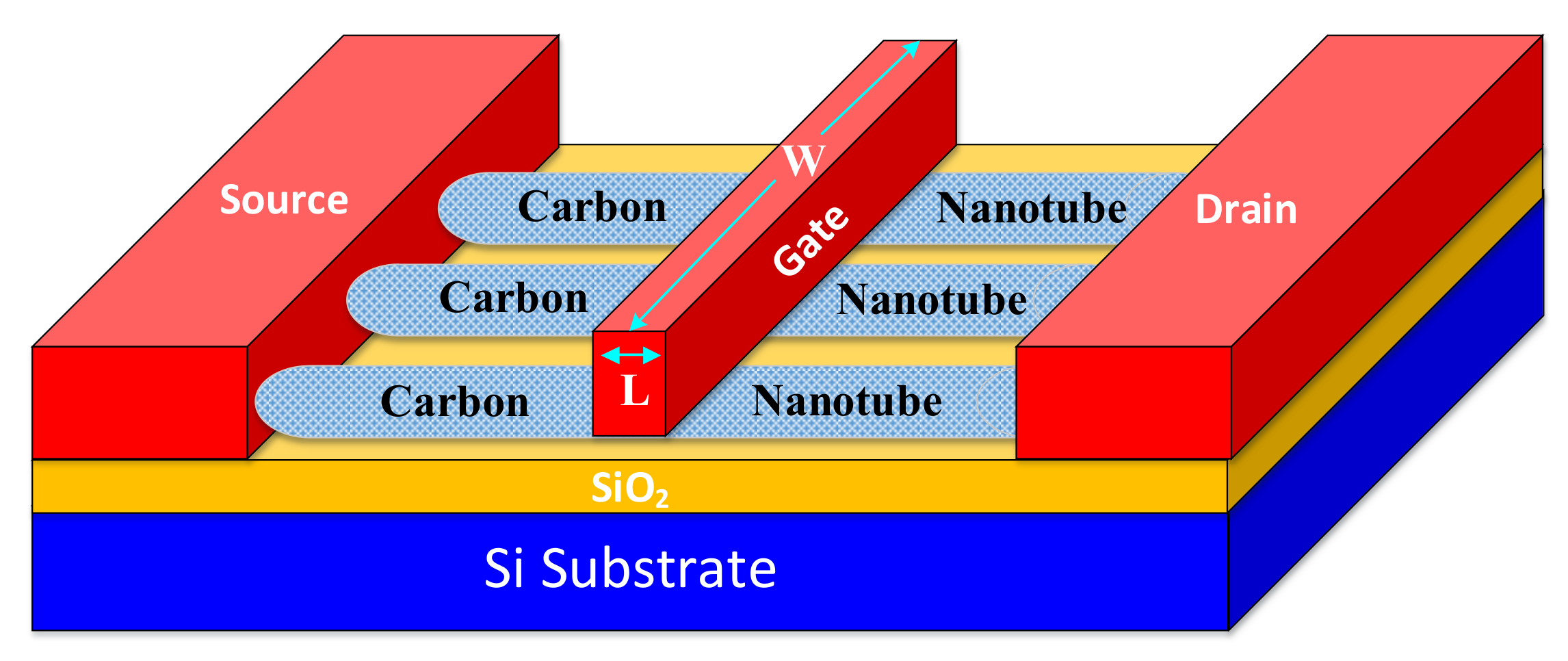
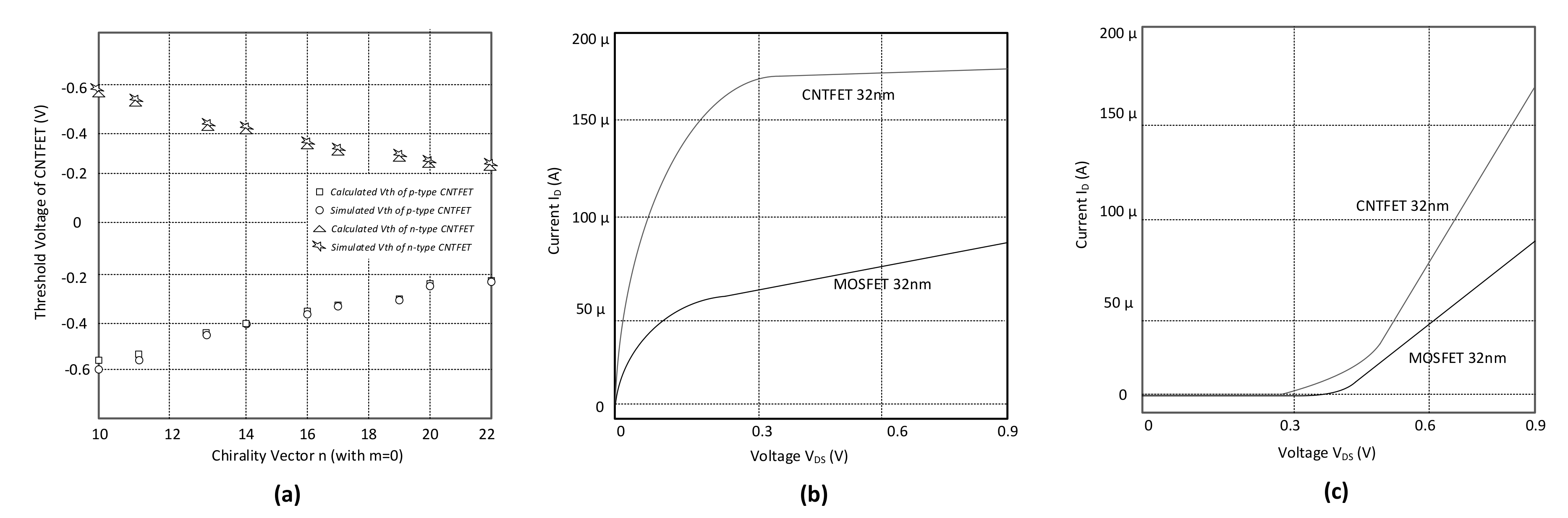
2. Carbon Nanotube Field Effect Transistors
Carbon Nanotubes (CNTs) came into existence in 1991 and the credit for its discovery was given to a Japanese physicist, S. lijima [24]. CNT is a nanoscale tube that is made up of rolled sheets of graphene and it can be either single-walled (SWCNT) or multi-walled (MWCNT). SWCNT consists of a single nanotube, whereas MWCNT is made up of multiple nanotubes with interlayer spacing of 0.34 nm. SWCNTs exhibit various properties, such as quasi ballistic carrier transport and suppression of short channel effects because of the one-dimensional electron transport [25]. SWCNT can act as either a conductor or a semiconductor, depending upon the angle of atom arrangement along the CNT, and it is represented by an integer pair (n, m), called chirality vector. In addition, SWCNTs can be either semiconducting or metallic in nature, depending upon the indices (n, m), which specify the nature of carbon atoms along the tube [26]. The nanotube is metallic if n = m or n − m = 3i, where “i” is an integer; otherwise, the nanotube is semiconducting.
Figure 1 shows the schematic of CNTFET having SWCNT placed between the two electrodes. From the figure, we observe that the highly doped CNTs are placed between the gate and the source/drain electrodes. These heavily doped CNT segments offer low electrical resistance in the ON-state of the CNTFET. The undoped CNTs that are placed under the gate electrode serve as the channel. The CNTFET gate width can be obtained from Equation (1) as [27].
where M represents tube number of CNT, is the minimum value of gate width, and P is the pitch value, referring to the distance between two adjacent CNTs.
Figure 1.
Schematic of a Carbon Nanotube Field Effect Transistor (CNTFET).
In order to calculate the diameter of the CNT, we make use of Equation (2) as [28].
where = 0.142 nm is the distance between the neighbouring carbon atoms and n, m are the chirality vectors that specify the roll orientation of CNT. Therefore, Equation for in nanometers can be rewritten as Equation (3).
Similar to the traditional MOSFET, CNTFET has four terminals. The channel region of the device consists of undoped nanotubes, which are semiconducting in nature and are placed in the channel region beneath the gate, while the nanotubes that are highly doped, and the placement is between the source/drain terminals and the gate. The device can then be turned either on or off, depending on the potential applied to the gate. The threshold voltage of CNTFET [28] is expressed in Equation (4), as.
where e is the electron charge, represents bandgap, = 2.49 Å is the carbon atom distance, and = 3.033 eV is the carbon - bond energy in the tight bonding model.
From Equations (3) and (4), we observe that the threshold voltage of the CNTFET is controlled by the diameter of the CNT, which, in turn, depends upon the the chirality vector (n, m). Thus, by changing the chirality vector or the diameter of the CNT, it is possible to control the threshold voltage of CNTFET [29]. Figure 2a shows the threshold voltage of both p-type CNTFET and n-type CNTFET obtained from Equation (4), and HSPICE simulation for various chirality vectors (various n for m = 0). The threshold voltage distribution of n-type CNTFET is the same as the P-type CNTFET, but with opposite sign. CNTFETs provide a unique opportunity to control threshold voltage by changing the chirality vector, or the diameter of the CNT [5].
Figure 2.
(a) CNTFET threshold variation with varying n (for m = 0). (b) Comparison of I–V curve of n-type MOSFET with n-type CNTFET in 32 nm technology for -. (c) Linear scale -.
Figure 2 depicts the characteristics current-voltage curve of an n-type MOSFET in 32 nm technology and a n-type CNTFET in 32 nm technology. From Figure 2b, we observe that the - characteristics of 32 nm CNTFET are more desirable when compared to that of a 32 nm MOSFET. In addition, from Figure 2c, we observe that the - curve of CNTFET is quadratic in saturation region, as compared to the linear - characteristics of MOSFET. This signifies that CNTFET has a higher transconductance () in comparison to that of MOSFET.
3. Circuit Level Implementation of Ternary Logic
For an existing binary system, voltage levels 0 V and are represented by two logic values ’0’ and ’1’, respectively. For the case of ternary systems, voltage levels 0 V, , and represent logic values ’0’, ’1’, and ’2’, respectively.
By utilizing ternary logic in design of digital systems, energy efficiency and simplicity can be achieved due to the reduced interconnect complexity as well as the chip area [30], therefore resulting in smaller power delay [31]. In addition, the transmission channels can be better utilized due to the higher storage density of each line. Additionally, the serial and serial-parallel arithmetic operations can be carried out faster by employing ternary logic. The numbers are represented in MVL systems in a balanced mode representation and unbalanced mode representation. However, the balanced mode representation is not used quite often, as it becomes difficult to deal with the negative voltages.
Let us assume that ternary values to represent false, undefined, and true conditions are 0, 1, and 2, respectively. Any ternary function of n variables () is defined as a logic function mapping from to {0, 1, 2}. The fundamental ternary logic operations are defined in Equation (5), as [32].
where , , and ’-’ represent the arithmetic subtraction. ’’ refers to the logical NOT operation, whereas ’’ and ’’ represent logical AND and logical OR operations, respectively. Table 1 shows the logic symbols that we assume for ternary logic design.
Table 1.
Logic Symbols.
In ternary logic, there exist modal functions and combinations, where n is a variable. When n = 1, we have one-variable functions f(y), and there are = 27 modal functions, called Literals. If n = 2, there are = 19,683 two variable functions. Literal is denoted by , where = 0, 1, 2, 01, 02 and 12 defined in Equations (6)–(13) as [33].
This paper focuses on utilizing CNTFET-RRAM ternary logic gates, a modified level shifter circuit and negation of literals technique in order to reduce the number of devices required for representing combinational logic functions. In addition, the negation of literals () that is given by Equations (14)–(18) is quite useful in reducing the number of ternary gates.
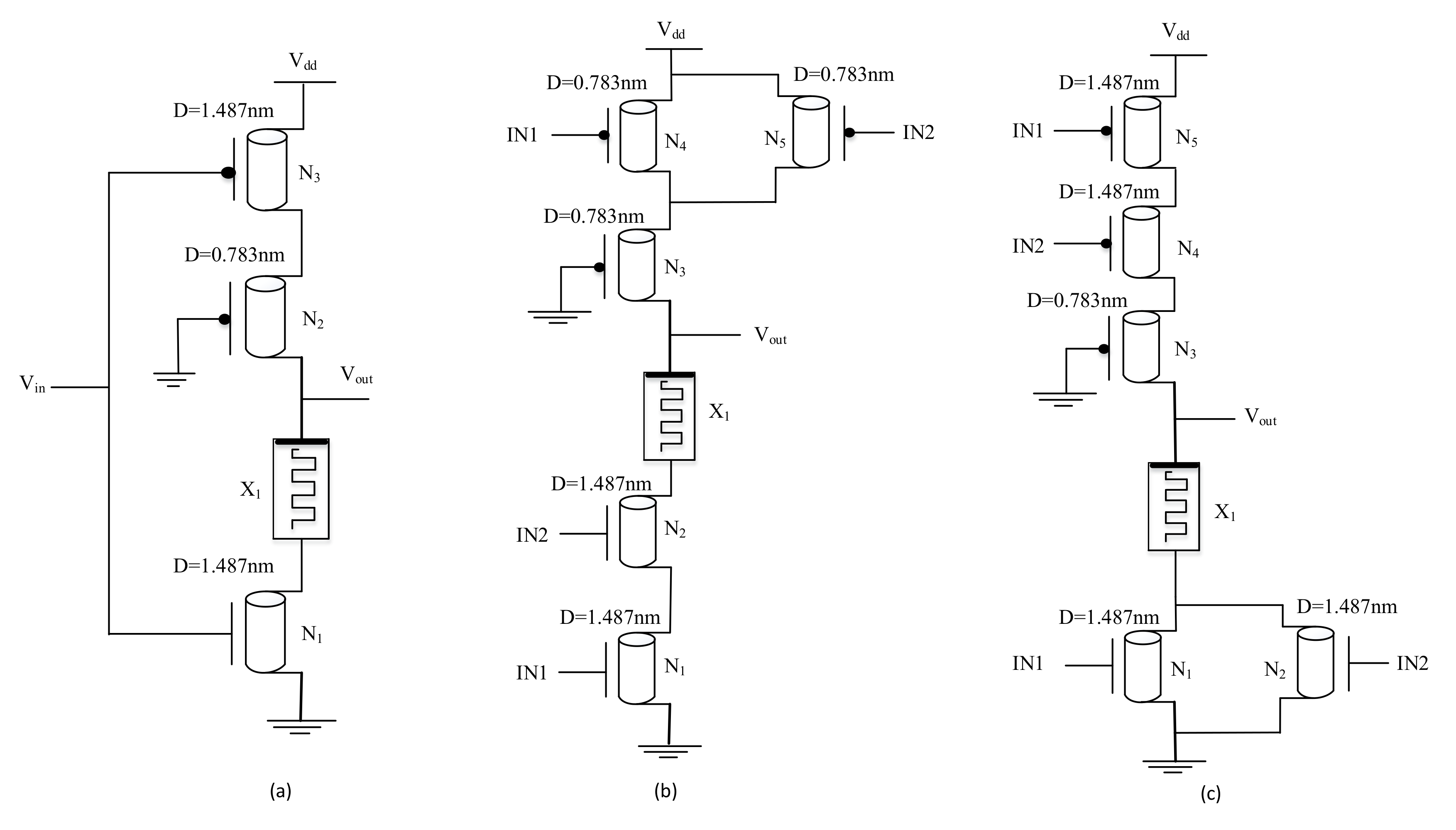
3.1. Overview of CNTFET-RRAM Ternary Logic Gates
Ternary logic gates that are designed using CNTFET-RRAM show improved performance in terms of lower power consumption, as the use of large resistors in the circuit is avoided, which resulted in higher power dissipation. For the design of digital systems, the basic gates are inverters, and the universal gates, i.e., NAND gates and NOR gates. Figure 3 depicts the logic symbols used for representing the basic ternary logic gates (Standard ternary inverter (STI), positive ternary inverter (PTI), negative ternary inverter (NTI), TNAND, and TNOR). Ternary inverters are classified, as: standard ternary inverter (STI), positive ternary inverter (PTI), and negative ternary inverter (NTI). For STI, three different logic levels (0, 1, and 2) are used in order to represent ternary numbers; whereas, for the case of PTI and NTI, we have only two logic levels (0 and 2) at the output corresponding to the three different logic levels at the input [33]. The STI, PTI, and NTI functions are given by Equations (19)–(21), as.
Figure 3.
Symbols of Ternary Logic Gates: (a) Standard ternary inverter (STI); (b) positive ternary inverter (PTI); (c) negative ternary inverter (NTI); (d) TNAND; and, (e) TNOR [17].
For the case of ternary NAND and ternary NOR, the outputs for the inputs and are given by Equations (22) and (23), respectively.
Figure 4a shows the circuit structure of CNTFET-RRAM based STI (Standard Ternary Inverter) previously described in [17]. The circuit is composed of two CNTFETs (, ), p-type CNTFET (with gate connected to the ground), () and RRAM device (). The CNTs , , and have chirality (19, 0), (10, 0), and (19, 0), respectively. From Equation (2), the diameters of , , and are 1.487 nm, 0.783 nm, and 1.487 nm, respectively. Therefore, from Equation (4), the threshold voltages of , , and are 0.293 V, −0.557 V, and −0.293 V, respectively. The number of tubes used for and is 3, while for is 1.
Figure 4.
Schematic of (a) STI; (b) Ternary NAND; and, (c) Ternary NOR [17].
The noise margin of the STI is determined graphically by plotting the voltage transfer curve of the ternary inverter. The VTC of the CNTFET-RRAM based STI is depicted in Figure 5. In ternary logic, four noise margins (, , , ) are specified for four voltage points (, , , ), as shown in the VTC curve. The static noise margin (SNM) of the STI is the smallest one among the four noise margins (, , , ). Table 2 presents the benchmarking of the proposed and the existing STI designs regarding the SNM.
Figure 5.
Voltage transfer curve (VTC) of Standard ternary inverter (STI) circuit.
Table 2.
Noise Margin values for STI designs.
CNTFET-RRAM ternary NAND and NOR gate schematic is depicted in Figure 4b,c, respectively. CNT chirality used in , , , is (19, 0) while for is (10, 0) for both the ternary NAND and NOR gates. The number of tubes used for , , , and is three while, for , is one.
The existing CNTFET-RRAM ternary gates can be implemented for the design of various arithmetic and combinational ternary logic designs. Despite significant progress, CNTFETs were until recently fabricated only in academic or research laboratories. However, a standard solution-based method that significantly improves the throughput, while simultaneously reducing the cost has been discovered, which allows for fabricating CNTFETs in a commercial silicon manufacturing facility with industry standard 200 mm wafers, employing the same equipment that is currently being used to fabricate silicon product wafers. Two different industry manufacturing facilities have reported successful fabrication of CNTFETs (i) a commercial silicon manufacturing facility (Analog Devices, Inc., Norwood, MA, USA, with more than 43,000 different products in production) and (ii) a high-volume manufacturing semiconductor foundry (Sky Water Technology, a US-based semiconductor foundry with more than 12,000 wafer starts per month capacity). The CNTFETs were fabricated while using the same equipment currently being used to fabricate silicon product wafers, explicitly demonstrating that CNTFET fabrication is Silicon-CMOS-compatible [35]. On the other hand, RRAM devices are CMOS-compatible and they can be fabricated with the existing state-of-the-art technology without the need of special equipment and materials. Thus, RRAM and CNTFETs can be built while using the traditional silicon-chip fabrication, which makes their integration feasible, thus making our designs more practically realizable.
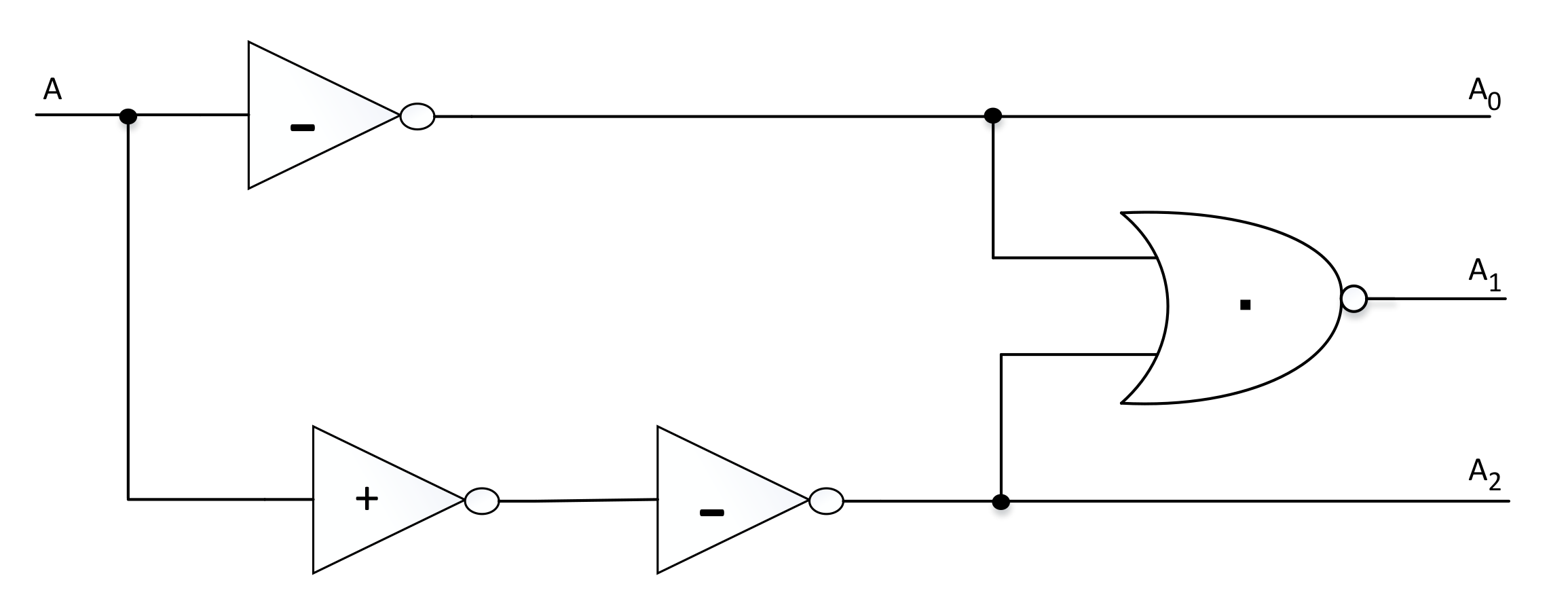
3.2. Ternary Decoder
The ternary decoder that is depicted in Figure 6 is a combinational logic circuit having a single input and three outputs that are represented by Equation (24) as [17]:
where n can have 0, 1, or 2 logic values. The decoder functions, as follows: if the input is 0, equals 2. If the input is 2, equals 2, and, if the input is 1, NOR gate makes = 2, because and are zero.
Figure 6.
Schematic of Ternary Decoder.
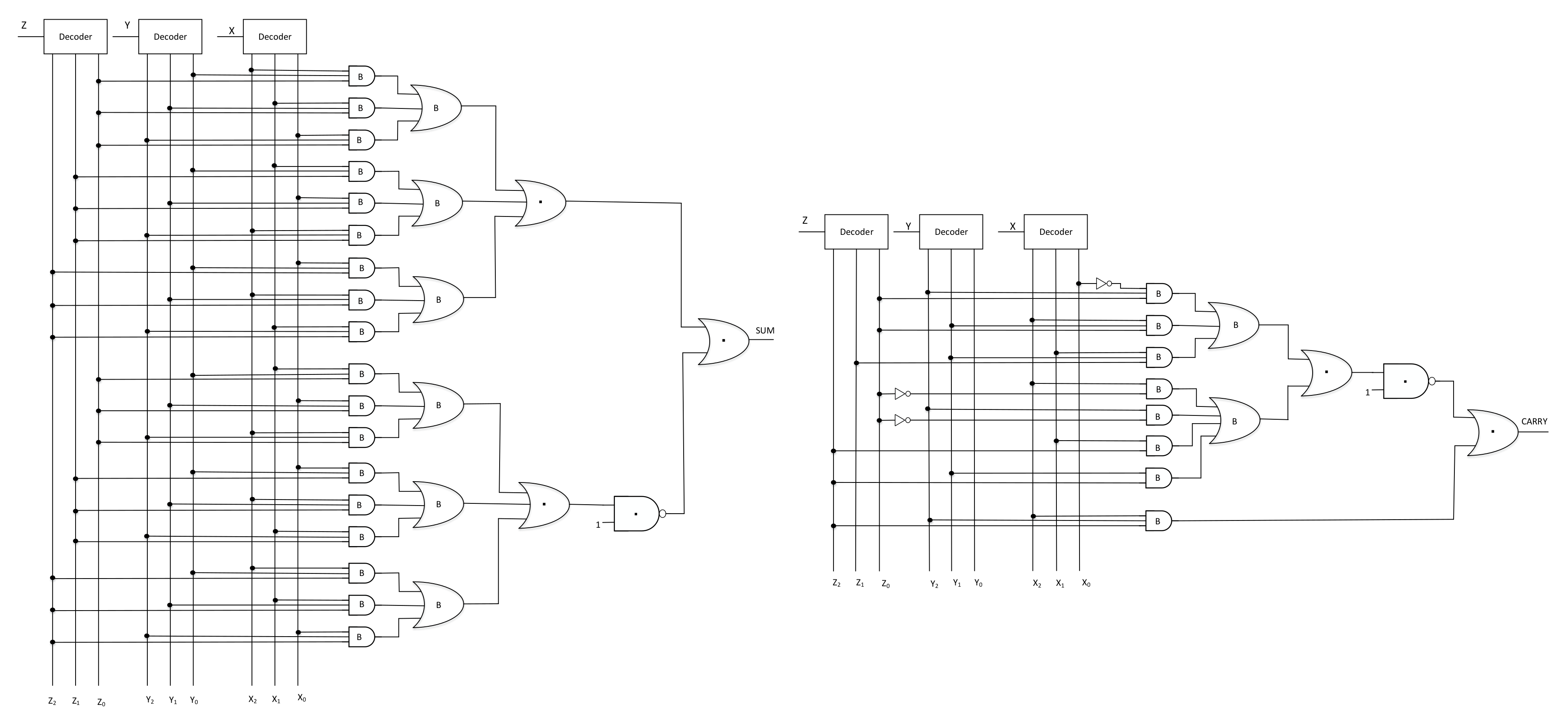
3.3. Ternary Half Adder
A ternary half adder is a combinational logic circuit that is depicted in Figure 7 that performs the addition of two bits and produces outputs sum and carry based on Equation (25) as [17].
Figure 7.
Schematic of Ternary Half Adder.
The equation for CARRY due to the negation of literals [33] is given in (26), as.
where and are the outputs of the ternary decoder to the inputs X and Y, respectively. The SUM and CARRY functions that are specified in Equations (25) and (26) are implemented while using the binary gates along with the CNTFET-RRAM ternary gates. A modified level shifter (LS) circuit that is shown in Figure 7 is implemented in order to obtain a logic function as:
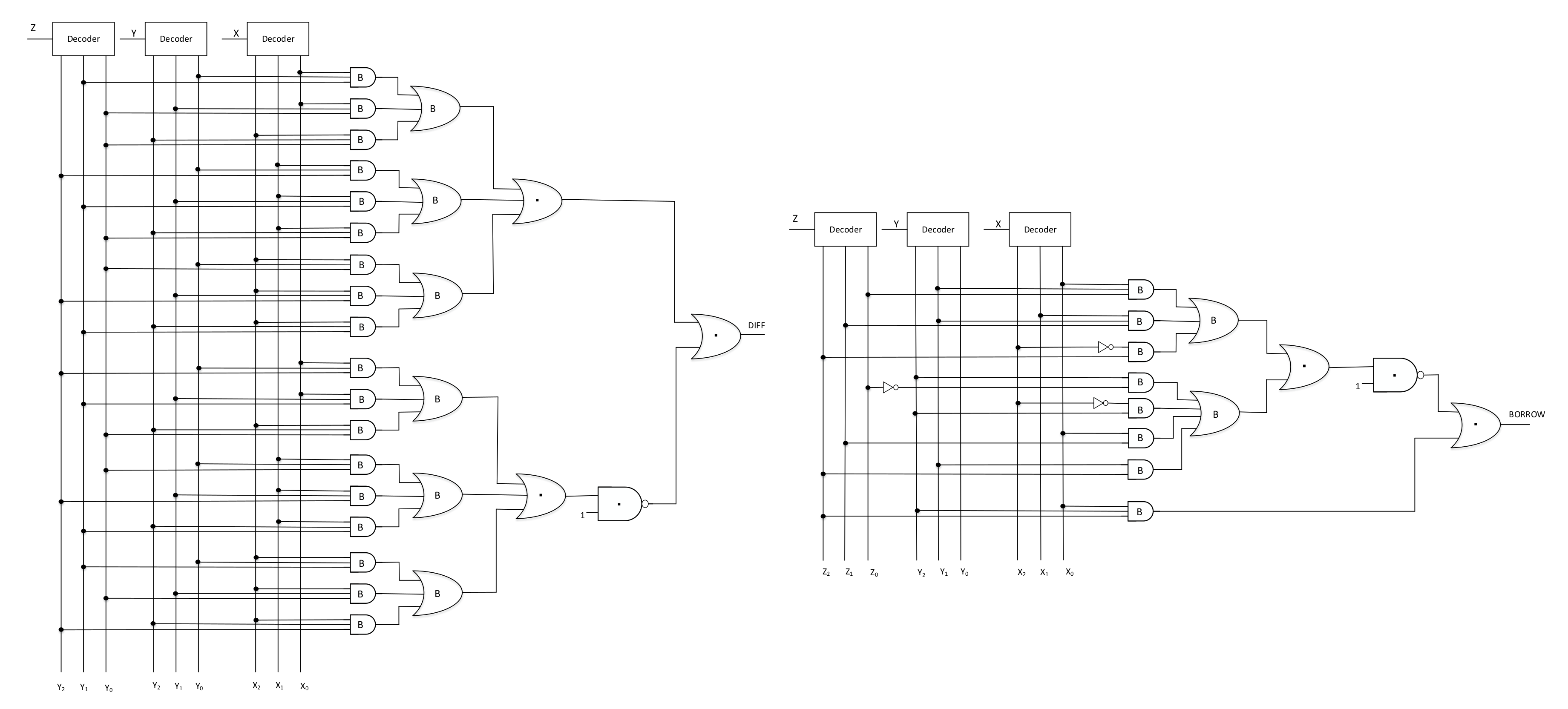
3.4. Ternary Half Subtractor
A ternary half subtractor that is shown in Figure 8 is a combinational circuit that subtracts one bit from the other and generates DIFFERENCE and BORROW outputs, which are based on Equation (28), as [17].
Figure 8.
Schematic of Ternary Half Subtractor.
The equation for BORROW due to the negation of literals [33] is given in (29), as.
where and are the outputs of the ternary decoder to the inputs X and Y, respectively. In this case, similar to the ternary half adder, the decoders X and Y generate the output signals, whereas the DIFFERENCE and BORROW functions that are specified in (28) and (29) are implemented using binary gates along with the CNTFET-RRAM ternary gates.
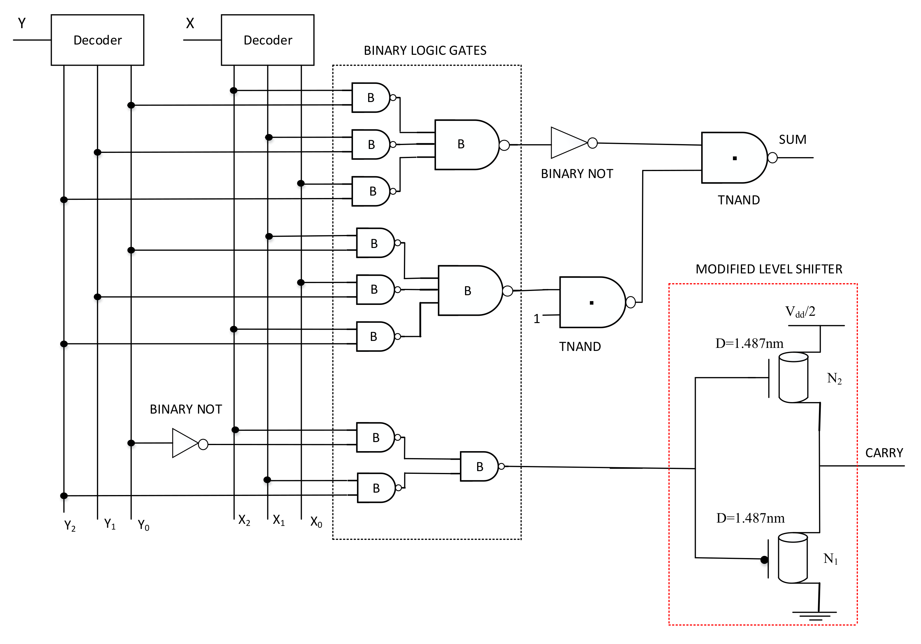
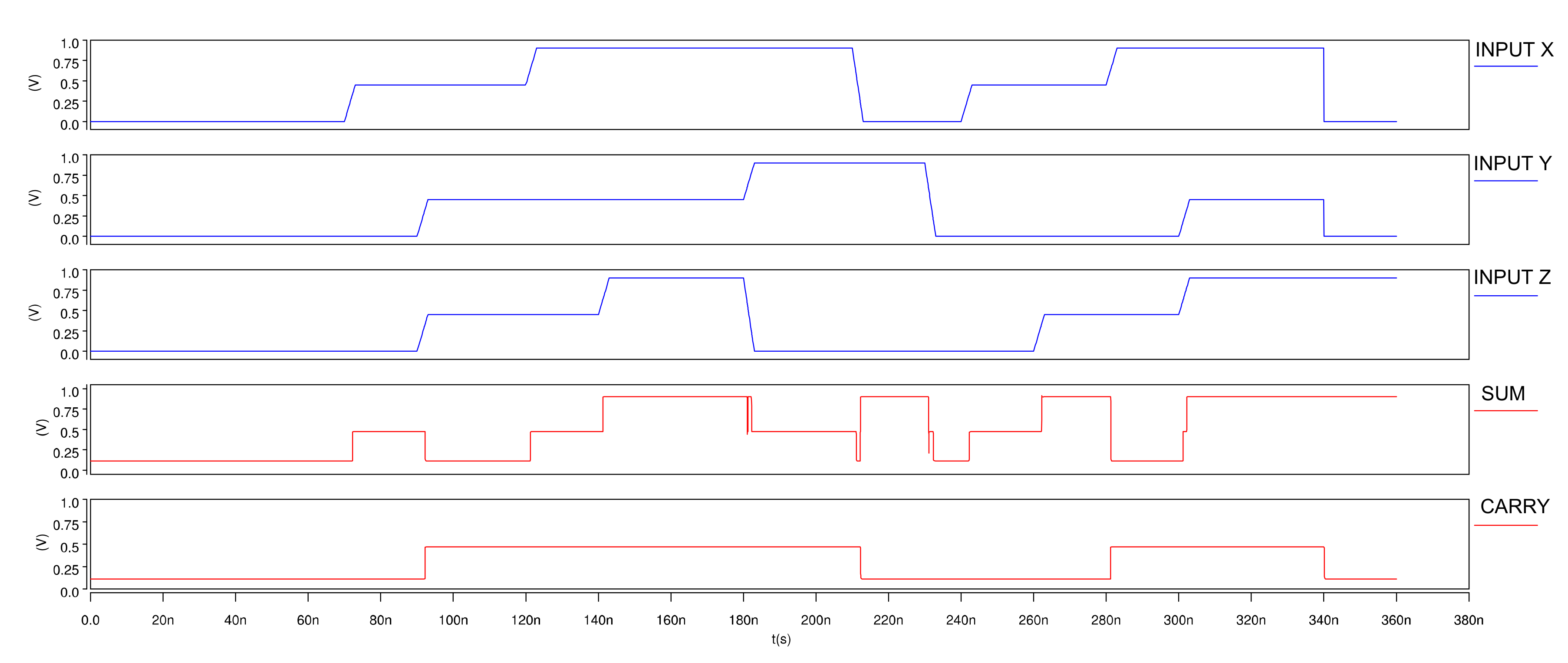
3.5. Ternary Full Adder
A ternary full adder circuit that is depicted in Figure 9 is a combinational logic circuit that is implemented while using ternary decoders, binary, and ternary logic gates. The circuit has inputs X, Y, Z and it produces SUM and CARRY outputs that are based on Equations (30) and (31).
Figure 9.
Schematic of Ternary Full Adder.
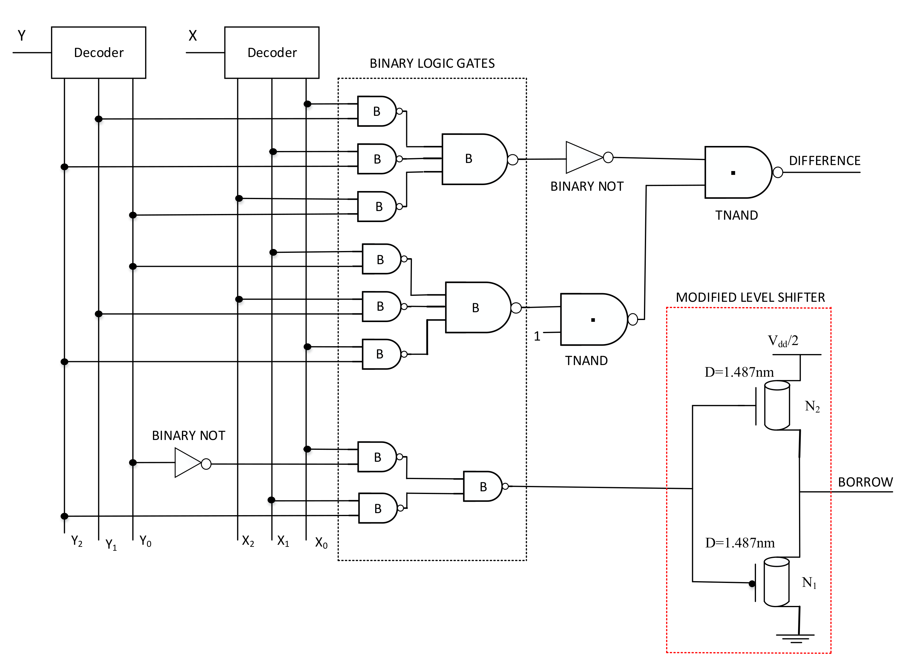
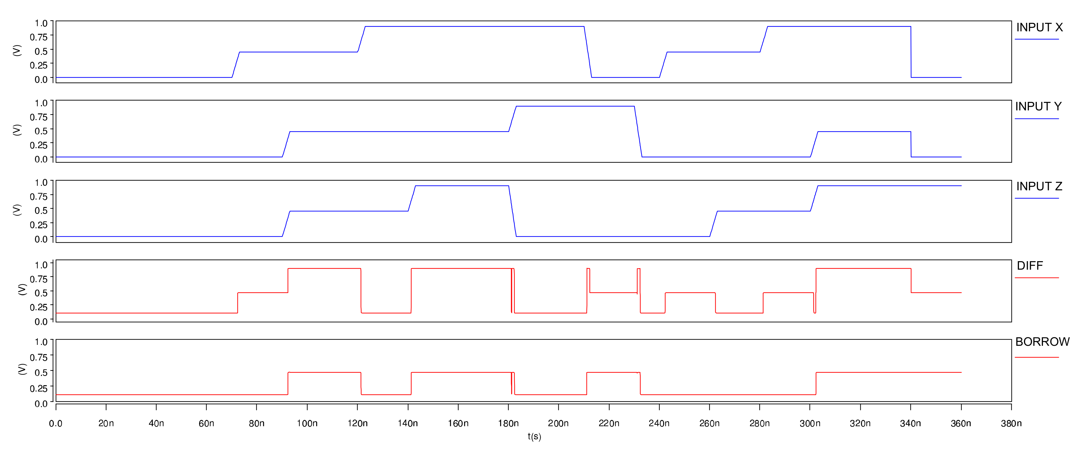
3.6. Ternary Full Subtractor
A ternary full subtractor circuit that is depicted in Figure 10 is a combinational logic circuit, which is implemented while using ternary decoders, binary, and ternary logic gates. The circuit has inputs X, Y, Z and it produces DIFFERENCE and BORROW outputs based on Equations (33) and (34).
Figure 10.
Schematic of Ternary Full Subtractor.
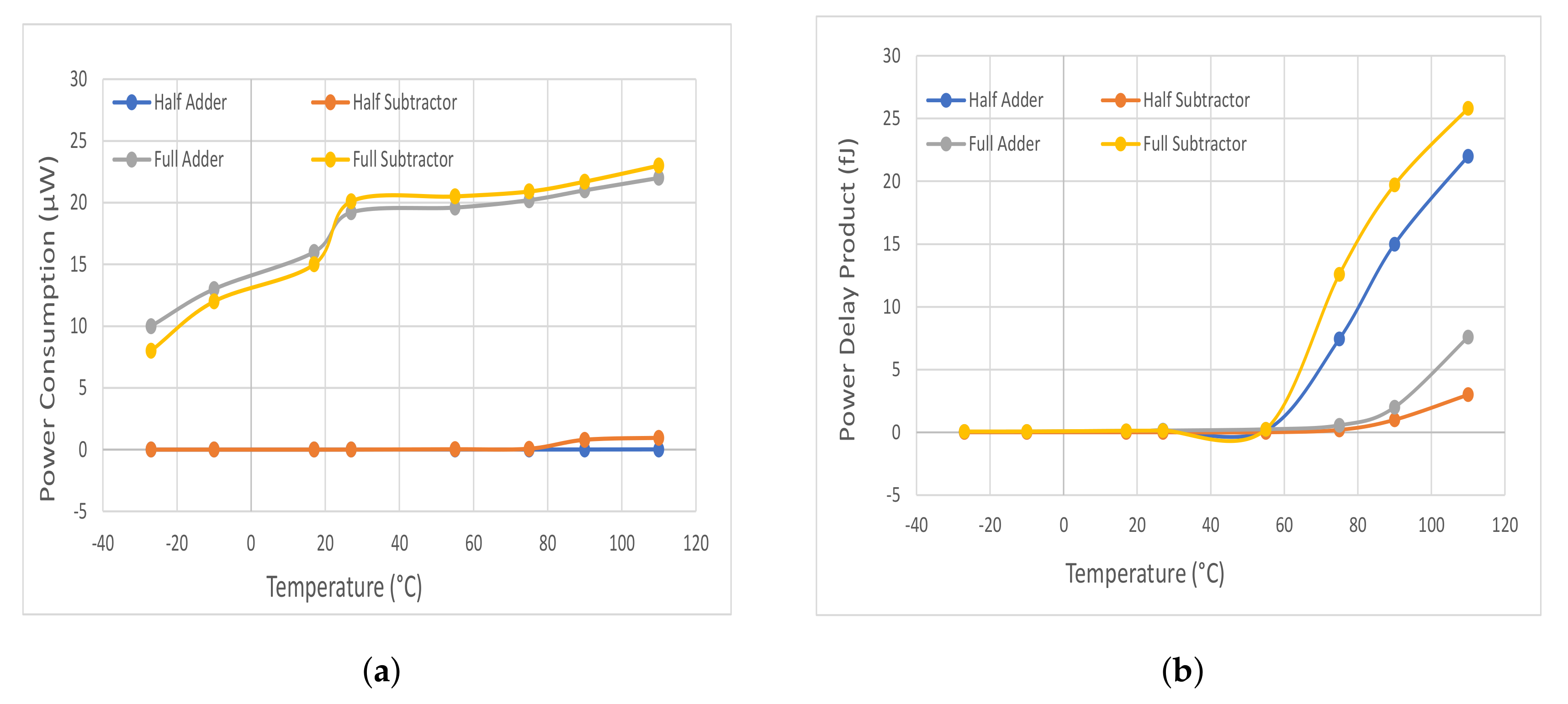
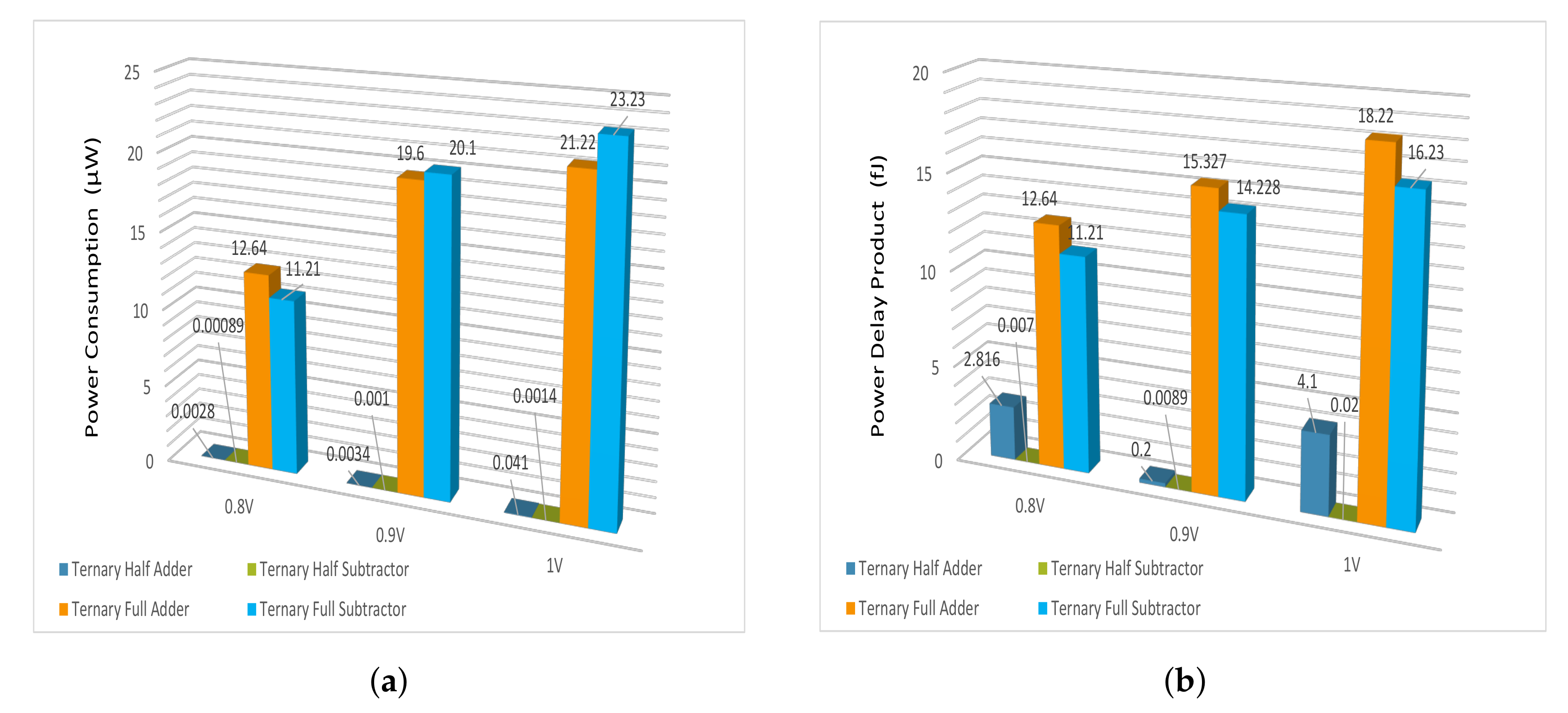
4. Results and Discussion
For simulation, 32-nanometre technology node, 0.9 V supply voltage at room temperature for all ternary designs is considered. The Stanford University CNTFET model [36] is implemented for analysis of all the designs in order to validate the operational performance. The Stanford model is SPICE compatible with channels that are composed of semiconducting single-walled carbon nanotubes having chirality that is user-specified and has channel length scaling effects that can be modelled down accurately to 20 nm. Table 3 lists the parameters of the CNTFET model and their values employed in the design. For RRAM, the Stanford University RRAM model [37] is employed. This RRAM model is physics-based spice compatible model that illustrates the switching performance of RRAM. This model is based on the growth of conductive filament (CF) and it includes the effect of critical phenomenon of switching, such as Joule heating and temperature change. The CF leaves a gap with the top electrode, which is called the filament gap. Thus, the rate of filament growth and filament gap govern the dynamics of this model. Table 4 provides a brief description of the RRAM parameters.
Table 3.
Characteristic parameters and their values employed for the Stanford University CNTFET model.
Table 4.
Characteristic parameters of Stanford University Resistive Random Access Memory (RRAM) model.
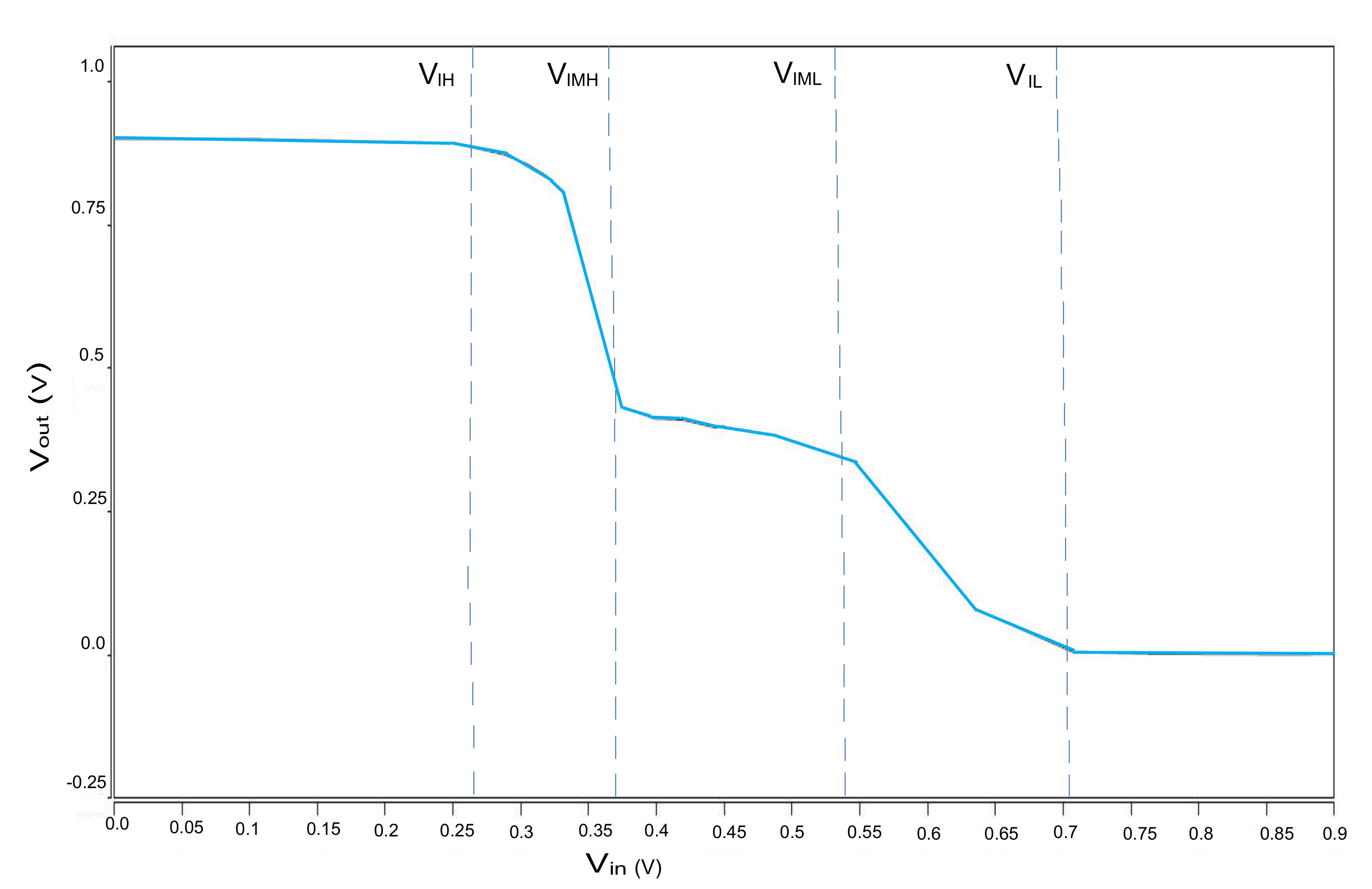
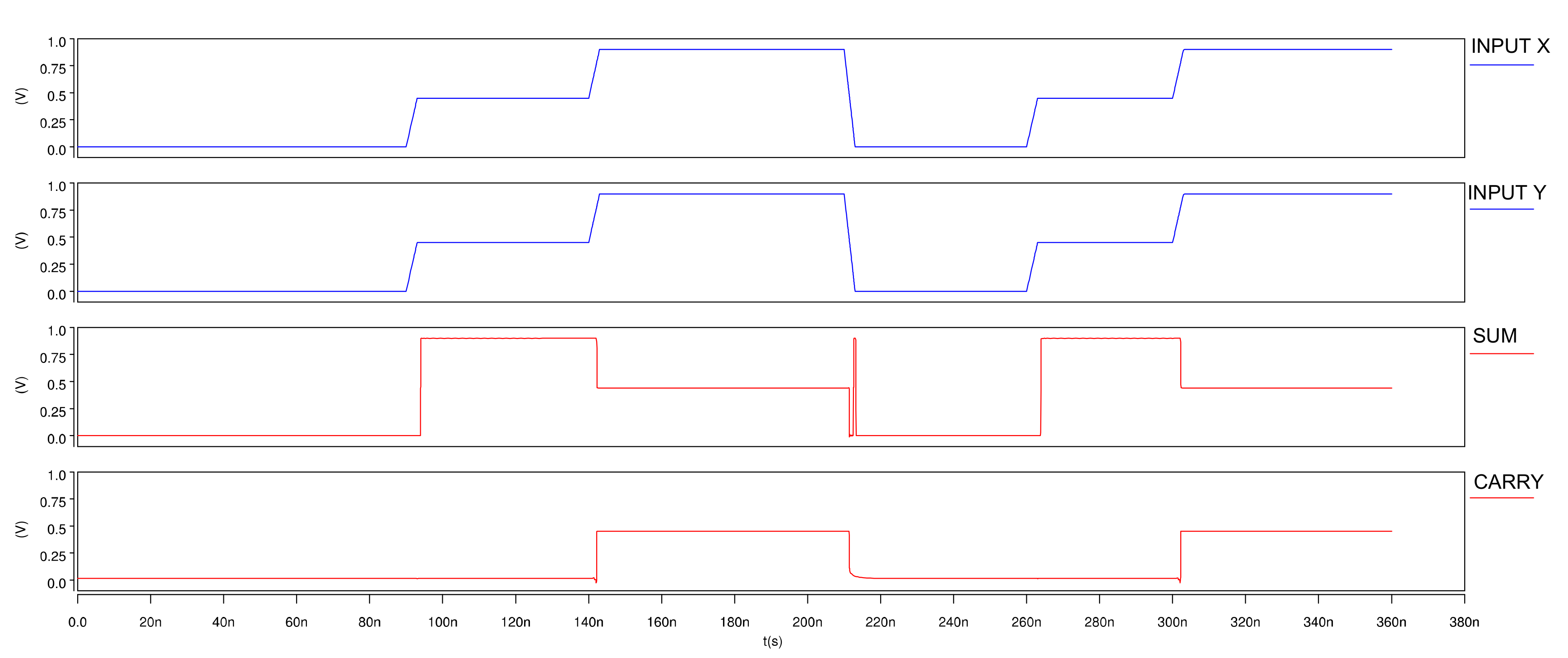
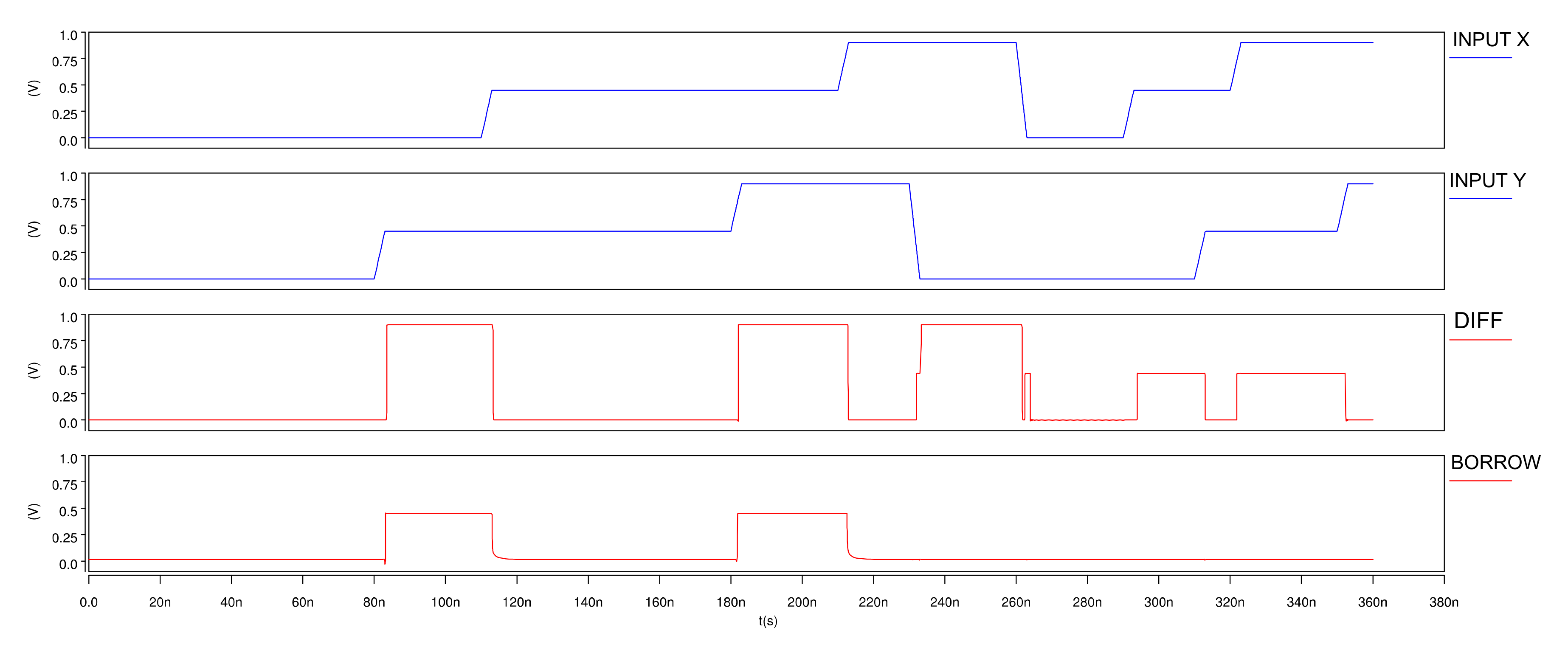
4.1. Functional Validation
The ternary circuits (half adder, half subtractor, full adder, and full subtractor) simulation is performed using HSPICE software. By utilizing the negation of literals technique, and the modified level shifter circuit, the proposed CNTFET-RRAM ternary combinational logic circuits achieve significant power savings. This is primarily due to the reduced component count as compared to the existing designs, which also results in a reduced area of the proposed circuits. For delay measurements, the delay values for all transitions are taken into account, and the average of the measurements is recorded as the average delay. In order to evaluate the power delay product (PDP), the power consumption and the average delay are multiplied. Table 5 lists the values that were obtained for power consumption, average delay, and power delay product obtained from HSPICE simulations.
Table 5.
Power Consumption, Delay, and Power Delay Product comparison for the ternary combinational logic circuits.
Figure 11 depicts the input and output waveforms for the proposed ternary half adder utilizing CNTFET-RRAM ternary logic gates. From the simulations performed using SPICE software, the power consumption and the delay are computed as 0.0034 μW and 25.11 ns, respectively. Therefore, the power delay product is computed to 0.085 fJ.
Figure 11.
Input and Output waveforms of Ternary Half Adder.
Figure 12 depicts the input and the output waveforms for the proposed ternary half subtractor utilizing CNTFET-RRAM ternary logic gates. From the simulations that were performed using SPICE software, the power consumption and the delay are computed as 0.00102 μW and 0.874 ns, respectively. Therefore, the power delay product is computed to 0.00089 fJ.
Figure 12.
Input and Output waveforms of Ternary Half Subtractor.
Figure 13 depicts the input and the output waveforms for the proposed ternary full adder utilizing CNTFET-RRAM ternary logic gates. From the simulations performed using SPICE software, the power consumption and the delay are computed as 19.6 μW and 0.782 ns, respectively. Therefore, the power delay product is computed to 15.327 fJ.
Figure 13.
Input and Output waveforms of Ternary Full Adder.
The input and the output waveforms for the proposed ternary full subtractor utilizing CNTFET-RRAM ternary logic gates is depicted in Figure 14. From the simulations performed using SPICE software, the power consumption and the delay are computed as 20.10 μW and 0.7079 ns, respectively. Therefore, the power delay product is computed as 14.228 fJ.
Figure 14.
Input and Output waveforms of Ternary Full Subtractor.
4.2. Performance Comparison
The schematic of ternary half adder and half subtractor circuits is composed of two ternary decoders, which are implemented while using CNTFET-RRAM ternary logic gates, nine two-inputs binary NAND, two three-inputs binary NAND, two binary inverters, two proposed two-inputs TNAND, and one proposed level shifter. Table 6 lists the component count (both transistors and RRAM) of the ternary half adder and the ternary half subtractor designs.
Table 6.
Component Count (transistors and RRAM) of the proposed Ternary Half Adder and Half Subtractor circuits.
Similarly, the schematic of ternary full adder and full subtractor circuits is composed of three ternary decoders, which are implemented while using CNTFET-RRAM ternary logic gates, four two-inputs binary AND, twenty two three-inputs binary AND, seven three-inputs binary OR, one four-inputs binary OR, two proposed three-inputs TOR, three proposed two-inputs TOR, two proposed two-inputs TNAND, and three binary inverters. Table 7 lists the component count (both transistors and RRAM) of the ternary full adder and the ternary full subtractor designs.
Table 7.
Component Count (transistors and RRAM) of the proposed Ternary Full Adder and Full Subtractor circuits.
The comparison of the transistor count for ternary half adder, ternary half subtractor, ternary full adder, and ternary full subtractor with the existing designs is depicted in Table 8. This comparison of the proposed circuits demonstrates a notable reduction in the transistors count. The reduction in the number of transistors of ternary half adder and half subtractor is 6.67% compared to the ternary half adder and ternary half subtractor in [17], 25% as compared to [28], 38.23% when compared to [32], 67.44% as compared to [33], 6.7% when compared to [42], and 25% as compared to [43].
Table 8.
Transistor count comparison of Ternary Combinational Logic circuits.
Similarly, for the case of ternary full adder and ternary full subtractor, the comparison is depicted in Table 7. For the ternary full adder and ternary full subtractor, transistor count reduction of around 13.14% as compared to the ternary full adder and full subtractor in [28], 18.20% when compared to [32], 51.71% as compared to [33], and 15.11% when compared to [43] is observed.
For realizing ternary half adder and ternary half subtractor, CNTFET-RRAM ternary logic gates are used and the design optimization is achieved by utilizing the negation of literals technique, in addition to the use of modified level shifter circuit. However, in the case of ternary full adder and ternary full subtractor circuits, we only use CNTFET-RRAM ternary logic gates and the negation of literals approach. The modified level shifter circuit employed in ternary half adder and ternary half subtractor designs in addition to having lesser transistors requires half the supply voltage (/2) as compared of the level shifter encoder circuit used in the previous reported designs, which also helps in reducing the power consumption. Thus, the power consumption of the ternary half adder and ternary half subtractor is significantly lower. The modified level shifter circuit cannot be incorporated in the ternary full adder and ternary subtractor designs, thus they have relatively higher power consumption, but, still, the power consumption values are comparable to the existing designs. However, the ternary full adder and the ternary full subtractor designs have significantly lower transistor count, due to the integration of CNTFET-RRAM technology and the added feature of non-volatility due to the presence of RRAM.
In this study, we also investigate the effect of varying the operating temperature on the circuit performance, as temperature is among the significant factors that negatively degrade the circuit performance. The effect of temperature variation on the performance metrics (power consumption and power delay product (PDP)) of ternary half adder, ternary half subtractor, ternary full adder, ternary full subtractor circuits, respectively, and the same is depicted in Figure 15a,b, respectively. From the observations, we conclude that there is a small variation in the power consumption and PDP over wide temperature ranges, thus having a negligible effect on circuit performance.
Figure 15.
Effect of varying operating temperature on (a) Power Consumption (b) Power Delay Product.
Similarly, we study the performance of the proposed ternary combinational logic circuits, with different supply voltages. Figure 16a,b demonstrates the effect of variation of supply volatge on the power consumption and power delay product of the proposed ternary half adder, ternary half subtractor, ternary full adder, and ternary full subtractor circuits, respectively. The results that were obtained from the simulations, show minimum variation in performance metrics of the proposed ternary designs with varying supply voltage.
Figure 16.
Effect of varying operating voltage on (a) Power Consumption (b) Power Delay Product.
Although digital circuits are inherently noise-tolerant, they are only affected by noises with high amplitude and wide width. We take the plot of Noise Immunity Curve (NIC) into account in order to determine the effect of input noise on the ternary half adder circuit. The noise signal depicted in Figure 17a, having pulse width () and pulse amplitude (), is injected into the inputs of ternary half adder. Figure 17b, depicts the NIC for the CNTFET-RRAM ternary half adder. Each point on the NIC represents a pair of (, ), above which the output will have an error. The region above the NIC point is an unsafe zone, whereas the region below is a safe zone against noise pulses. Thus, any circuit with higher NIC demonstrates a more noise tolerant circuit. From the NIC, we conclude that the proposed CNTFET-RRAM ternary half adder circuit demonstrates a good tolerance to the input noise sources.
Figure 17.
Plot of (a) Input Noise Signal (b) Noise Immunity Curve (NIC).
5. Conclusions
The implementation of computing systems utilizing ternary logic designs has come to the fore in recent years, owing to the significant research that has focussed on emerging technologies. This manuscript utilizes the CNTFET and RRAM for implementing combinational ternary logic circuits. The proposed ternary designs (half adder, half subtractor, full adder, and full subtractor) have been implemented and simulated wile using HSPICE and the results obtained from the simulation confirm the proper functionality of the proposed designs. When compared to the existing designs, the proposed ternary designs are superior in terms of the transistor count, power consumption, and reduced area. Therefore, on the basis of the results that were obtained from the simulations, we deduce that the proposed methodology is an effective solution for reducing the component count, complexity of the hardware, power consumption, and cost of the design. In addition, the proposed designs are analyzed under various operating conditions, with varying supply voltages and different operating temperatures, in order to confirm the robustness of the designs.
Author Contributions
Conceptualization, F.Z., F.A.H., and F.A.K.; methodology, F.Z., F.A.H., and F.A.K.; software, F.Z.; validation, F.A.H., and F.A.K., and F.Z.; formal analysis, M.R.A., and I.M.N.; investigation, F.Z., F.A.H., and F.A.K.; resources, F.A.H., M.R.A., and I.M.N.; writing-original draft preparation, F.Z.; writing-review and editing, F.A.H., F.A.K., M.R.A., I.M.N., C.Y.O., F.Z.R.; visualization, M.R.A., I.M.N., C.Y.O., F.Z.R.; supervision, F.A.H.; project administration, F.A.H.; funding acquisition, F.Z., F.A.H. and F.A.K.; All authors have read and agreed to the published version of the manuscript.
Funding
This work was funded and supported by Yayasan Universiti Teknologi PETRONAS (YUTP)-Fundamental Research Grant with cost centre 015LC0-245.
Acknowledgments
The authors would like to thank the editorial board and reviewers for their suggestions which helped improve the technical content of this manuscript.
Conflicts of Interest
The authors declare no conflict of interest.
Abbreviations
The following abbreviations are used in this manuscript:
| RRAM | Resistive Random Access Memory |
| CNTFET | Carbon Nanotube Field Efect Transistors |
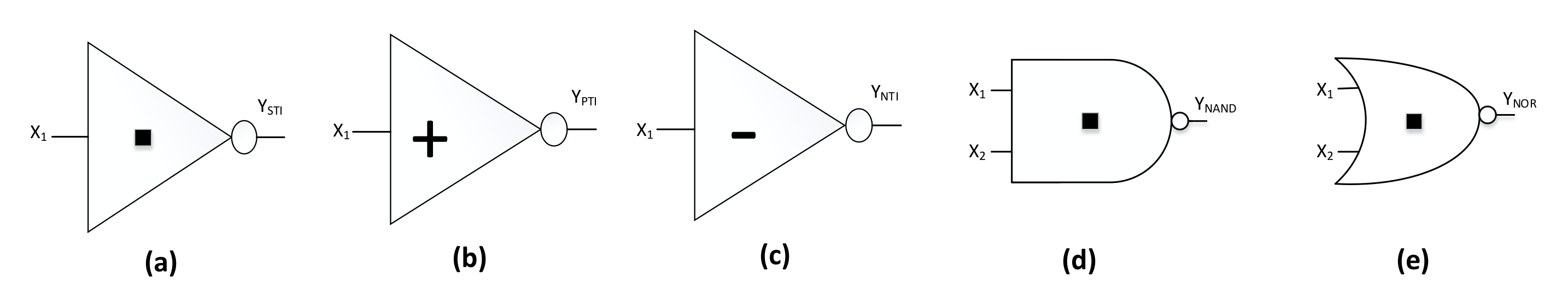
| STI | Standard Ternary Inverter |
| NTI | Negative Ternary Inverter |
| PTI | Positive Ternary Inverter |
| NIC | Noise Immunity Curve |
References
- Sharma, T.; Kumre, L. Energy-Efficient Ternary Arithmetic Logic Unit Design in CNTFET Technology. Circuits Syst. Signal Process. 2019, 39, 3265–3288. [Google Scholar] [CrossRef]
- Vudadha, C.; Katragadda, S.; Phaneendra, P.S. 2: 1 Multiplexer based design for ternary logic circuits. In Proceedings of the 2013 IEEE Asia Pacific Conference on Postgraduate Research in Microelectronics and Electronics (PrimeAsia), Visakhapatnam, India, 19–21 December 2013. [Google Scholar]
- Murotiya, L.S.; Gupta, A. Design of CNTFET-based 2-bit ternary ALU for nanoelectronics. Int. J. Electron. 2014, 101, 1244–1257. [Google Scholar] [CrossRef]
- Chen, L.J.L.; Han, J.; Lombardi, F. Design and evaluation of multiple valued logic gates using pseudo N-type carbon nanotube FETs. IEEE Trans. Nanotechnol. 2014, 13, 695–708. [Google Scholar]
- Lin, S.; Kim, Y.-B.; Lombardi, F. Design of a ternary memory cell using CNTFETs. IEEE Trans. Nanotechnol. 2012, 11, 1019–1025. [Google Scholar]
- Levashenko, Z.E.V.; Lukyanchuk, I.; Rabcan, J.; Kvassay, M.; Rusnak, P. Application of Generalized Reed-Muller Expression for Development of Non-Binary Circuits. Electronics 2020, 9, 12. [Google Scholar]
- Moaiyeri, M.H.; Shamohammadi, M.; Sharifi, F.; Navi, K. High-performance ternary logic gates for nanoelectronics. Int. J. High Perform. Syst. Archit. 2015, 5, 209–215. [Google Scholar] [CrossRef]
- Prakash, P.; Sundaram, K.M.; Bennet, M.A. A review on carbon nanotube field effect transistors (CNTFETs) for ultra-low power applications. Renew. Sustain. Energy Rev. 2018, 89, 194–203. [Google Scholar] [CrossRef]
- Obite, F.; Ijeomah, G.; Bassi, J.S. Carbon nanotube field effect transistors: Toward future nanoscale electronics. Int. J. Comput. Appl. 2019, 41, 149–164. [Google Scholar] [CrossRef]
- Hu, Z.; Tulevski, G.S.; Hannon, J.B.; Afzali, A.; Liehr, M.; Park, H. Variability and reliability analysis in self-assembled multichannel carbon nanotube field-effect transistors. Appl. Phys. Lett. 2015, 106, 243106. [Google Scholar] [CrossRef]
- Khurshid, T.; Fatima, S.; Khanday, F.A.; Bashir, F.; Zahoor, F.; Hussin, F.A. Carbon nanotube field effect transistor (CNTFET) operational transconductance amplifier (OTA) based design of high frequency memristor emulator. Int. J. Numer. Model. Electron. Netw. Devices Fields 2020, 2827. [Google Scholar] [CrossRef]
- Banerjee, W. Challenges and Applications of Emerging Nonvolatile Memory Devices. Electronics 2020, 9, 1029. [Google Scholar] [CrossRef]
- Lim, E.W.; Ismai, R. Conduction Mechanism of Valence Change Resistive Switching Memory: A Survey. Electronics 2015, 4, 586–613. [Google Scholar] [CrossRef]
- Arumi, D.; Manich, S.; Gomez-Pau, A.; Rodriguez-Montanes, R.; Montilla, V.; Hernandez, D.; Gonzalez, M.B.; Campabadal, F. Impact of Laser Attacks on the Switching Behavior of RRAM Devices. Electronics 2020, 9, 200. [Google Scholar] [CrossRef]
- Perez, E.; Ossorio, O.G.; Duenas, S.; Castan, H.; Garcia, H.; Wenger, C. Programming Pulse Width Assessment for Reliable and Low-Energy Endurance Performance in Al:HfO2-Based RRAM Arrays. Electronics 2020, 9, 864. [Google Scholar] [CrossRef]
- Zahoor, F.; Zulkifli, T.Z.A.; Khanday, F.A. Resistive Random Access Memory (RRAM): An Overview of Materials, Switching Mechanism, Performance, Multilevel Cell (mlc) Storage, Modeling, and Applications. Nanoscale Res. Lett. 2020, 15, 90. [Google Scholar] [CrossRef]
- Zahoor, F.; Zulkifli, T.Z.A.; Khanday, F.A.; Murad, S.A.Z. Carbon Nanotube and Resistive Random Access Memory Based Unbalanced Ternary Logic Gates and Basic Arithmetic Circuits. IEEE Access 2020, 8, 104701–104717. [Google Scholar] [CrossRef]
- Shulaker, M.M.; Hills, G.; Park, R.S.; Howe, R.T.; Saraswat, K.; Wong, H.-S.P.; Mitra, S. Three-dimensional integration of nanotechnologies for computing and data storage on a single chip. Nature 2017, 547, 74–78. [Google Scholar] [CrossRef]
- Zhang, H.; Zhang, Z.; Gao, M.; Luo, L.; Duan, S.; Dong, Z.; Lin, H. Implementation of Unbalanced Ternary Logic Gates with the Combination of Spintronic Memristor and CMOS. Electronics 2020, 9, 542. [Google Scholar] [CrossRef]
- Zahoor, F.; Zulkifli, T.Z.A.; Khanday, F.A.; Fida, A.A. Low-power RRAM Device based 1T1R Array Design with CNTFET as Access Device. In Proceedings of the 2019 IEEE Student Conference on Research and Development (SCOReD), Bandar Seri Iskandar, Malaysia, 15–17 October 2019; pp. 280–283. [Google Scholar]
- Strukov, D.; Kohlstedt, H. Resistive switching phenomena in thin films: Materials, devices, and applications. MRS Bull. 2012, 37, 108–114. [Google Scholar] [CrossRef]
- Prabhu, N.L.; Jun, D.L.J.; Dananjaya, P.A.; Lew, W.S.; Toh, E.H.; Raghavan, N. Exploring the Impact of Variability in Resistance Distributions of RRAM on the Prediction Accuracy of Deep Learning Neural Networks. Electronics 2020, 9, 414. [Google Scholar] [CrossRef]
- Pan, F.; Gao, S.; Chen, C.; Song, C.; Zeng, F. Recent progress in resistive random access memories: Materials, switching mechanisms, and performance. Mater. Sci. Eng. R Rep. 2014, 83, 1–59. [Google Scholar] [CrossRef]
- Natsuki, T. Carbon Nanotube-Based Nanomechanical Sensor: Theoretical Analysis of Mechanical and Vibrational Properties. Electronics 2017, 6, 56. [Google Scholar] [CrossRef]
- Appenzeller, J. Carbon Nanotubes for High-Performance Electronics—Progress and Prospect. Proc. IEEE 2008, 96, 201–211. [Google Scholar] [CrossRef]
- Sethi, D.; Kaur, M.; Singh, G. Design and performance analysis of a CNFET-based TCAM cell with dual-chirality selection. J. Comput. Electron. 2017, 16, 106–114. [Google Scholar] [CrossRef]
- Moaiyeri, M.H.; Mirzaee, R.F.; Doostaregan, A.; Navi, K.; Hashemipour, O. A universal method for designing low-power carbon nanotube FET-based multiple-valued logic circuits. IET Comput. Digit. Tech. 2013, 7, 167–181. [Google Scholar] [CrossRef]
- Samadi, H.; Shahhoseini, A.; Aghaei-liavali, F. A new method on designing and simulating CNTFET based ternary gates and arithmetic circuits. Microelectron. J. 2017, 63, 41–48. [Google Scholar] [CrossRef]
- Jaber, R.A.; Kassem, A.; EL-Hajj, A.M.; EL-Nimri, L.A.; Haida, A.M. High-performance and energy-efficient CNFET-based designs for ternary logic circuits. IEEE Access 2019, 7, 93871–93886. [Google Scholar] [CrossRef]
- Rokhani, F.Z.; Sobelman, G.E. Bus Energy Consumption for Multilevel Signals. IEEE Trans. Circuits Syst. Regul. Pap. 2009, 57, 64–71. [Google Scholar] [CrossRef][Green Version]
- Soliman, N.; Fouda, M.E.; Alhurbi, A.G.; Said, L.A.; Madian, A.H.; Radwan, A.G. Ternary Functions Design Using Memristive Threshold Logic. IEEE Access 2019, 7, 48371–48381. [Google Scholar] [CrossRef]
- Lin, S.; Kim, Y.-B.; Lombardi, F. CNTFET-based design of ternary logic gates and arithmetic circuits. IEEE Trans. Nanotechnol. 2011, 10, 217–225. [Google Scholar] [CrossRef]
- Sridevi, V.; Jayanthy, T. Minimization of CNTFET ternary combinational circuits using negation of literals technique. Arab. J. Sci. Eng. 2014, 39, 4875–4890. [Google Scholar] [CrossRef]
- Mohammed, M.U.; Vijjapuram, R.; Chowdhury, M.H. Novel CNTFET and Memristor based Unbalanced Ternary Logic Gate. In Proceedings of the 2018 IEEE 61st International Midwest Symposium on Circuits and Systems (MWSCAS), Windsor, ON, Canada, 5–8 August 2018; pp. 1106–1109. [Google Scholar]
- Bishop, M.D.; Hills, G.; Srimani, T.; Lau, C.; Murphy, D.; Fuller, S.; Humes, J.; Ratkovich, A.; Nelson, M.; Shulaker, M.M. Fabrication of carbon nanotube field-effect transistors in commercial silicon manufacturing facilities. Nat. Electron. 2020, 3, 492–501. [Google Scholar] [CrossRef]
- Stanford CNFET Model. Available online: https://nano.stanford.edu/stanford-cnfet-model (accessed on 1 November 2020).
- Stanford RRAM Model. Available online: https://nano.stanford.edu/stanford-rram-model (accessed on 1 November 2020).
- Shahrom, E.; Hosseini, S.A. A new low power multiplexer based ternary multiplier using CNTFETs. AEU Int. J. Electron. Commun. 2018, 93, 191–207. [Google Scholar] [CrossRef]
- Das, S.; Bhattacharya, S.; Das, D. Design of digital logic circuits using carbon nanotube field effect transistors. Int. J. Soft Comput. Eng. 2011, 1, 173–178. [Google Scholar]
- Navi, K.; Momeni, A.; Sharifi, F.; Keshavarzian, P. Two novel ultra high speed carbon nanotube Full-Adder cells. IEICE Electron. Express 2009, 6, 1395–1401. [Google Scholar] [CrossRef]
- Navi, K.; Rashtian, M.; Khatir, A.; Keshavarzian, P.; Hashemipour, O. High speed capacitor-inverter based carbon nanotube full adder. Nanoscale Res. Lett. 2010, 5, 859–862. [Google Scholar] [CrossRef][Green Version]
- Jaber, R.A.; El-Hajj, M.; Kassem, A.; Nimri, L.A.; Haidar, A.M. CNFET-based designs of ternary half-adder using a novel ‘decoder-less’ ternary multiplexer based on unary operators. Microelectron. J. 2019, 96, 104698. [Google Scholar] [CrossRef]
- Sandhie, Z.T.; Ahmed, F.U.; Chowdhury, M.H. Design of Ternary Logic and Arithmetic Circuits using GNRFET. IEEE Open J. Nanotechnol. 2020, 1, 77–87. [Google Scholar] [CrossRef]
Publisher’s Note: MDPI stays neutral with regard to jurisdictional claims in published maps and institutional affiliations. |
© 2021 by the authors. Licensee MDPI, Basel, Switzerland. This article is an open access article distributed under the terms and conditions of the Creative Commons Attribution (CC BY) license (http://creativecommons.org/licenses/by/4.0/).


