Power and Area Efficient Clock Stretching and Critical Path Reshaping for Error Resilience

Abstract
1. Introduction
- (1)
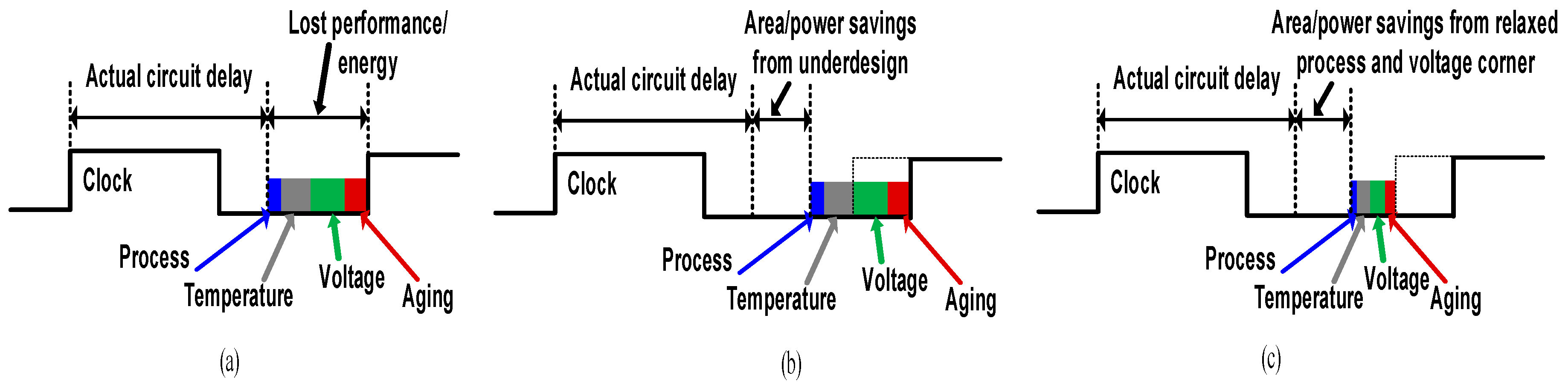
- We propose a simple clock stretcher to borrow slack available in the processor pipeline stage. Timing closure with pessimistic design margins with respect to the delayed clock prevents meta-stability and critical operating point behavior issues in the pipeline.
- (2)
- We come up with two critical path reshaping techniques to convert the extra slack margins created by the clock stretcher into power and area savings as shown in Figure 2b,c. The first approach relaxes the slack margins and redesigns the logic based on the new slack. The second approach replaces the logic library with BTWC sigma corner library.
- (3)
- The proposed approaches downsize the short path logic along with the critical paths, which removes hold buffer overheads. The non-speculative nature of our approach removes error management and latency overheads which minimizes the cost for error resilience.
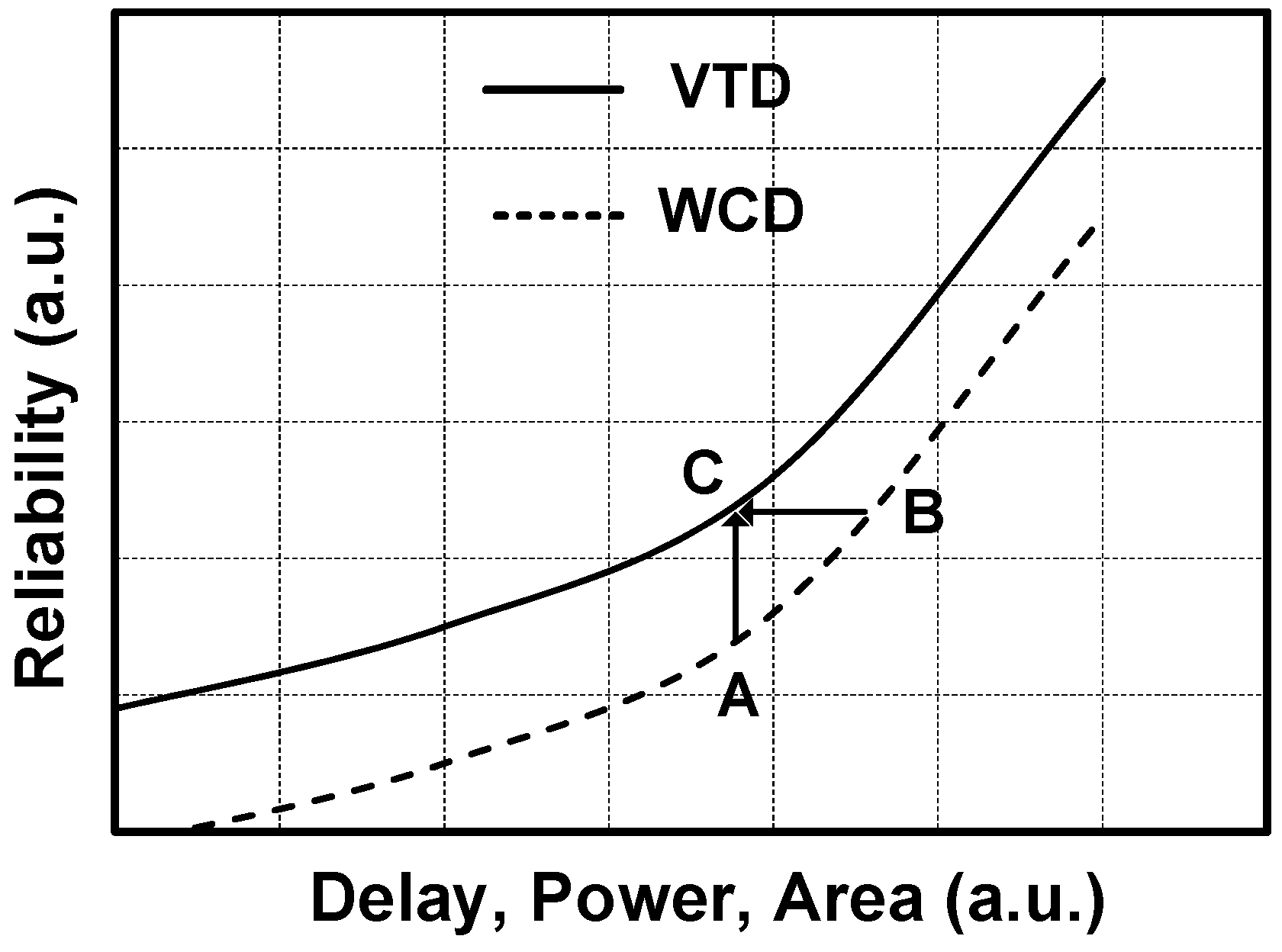
2. Motivation
3. Proposed Design Methodology
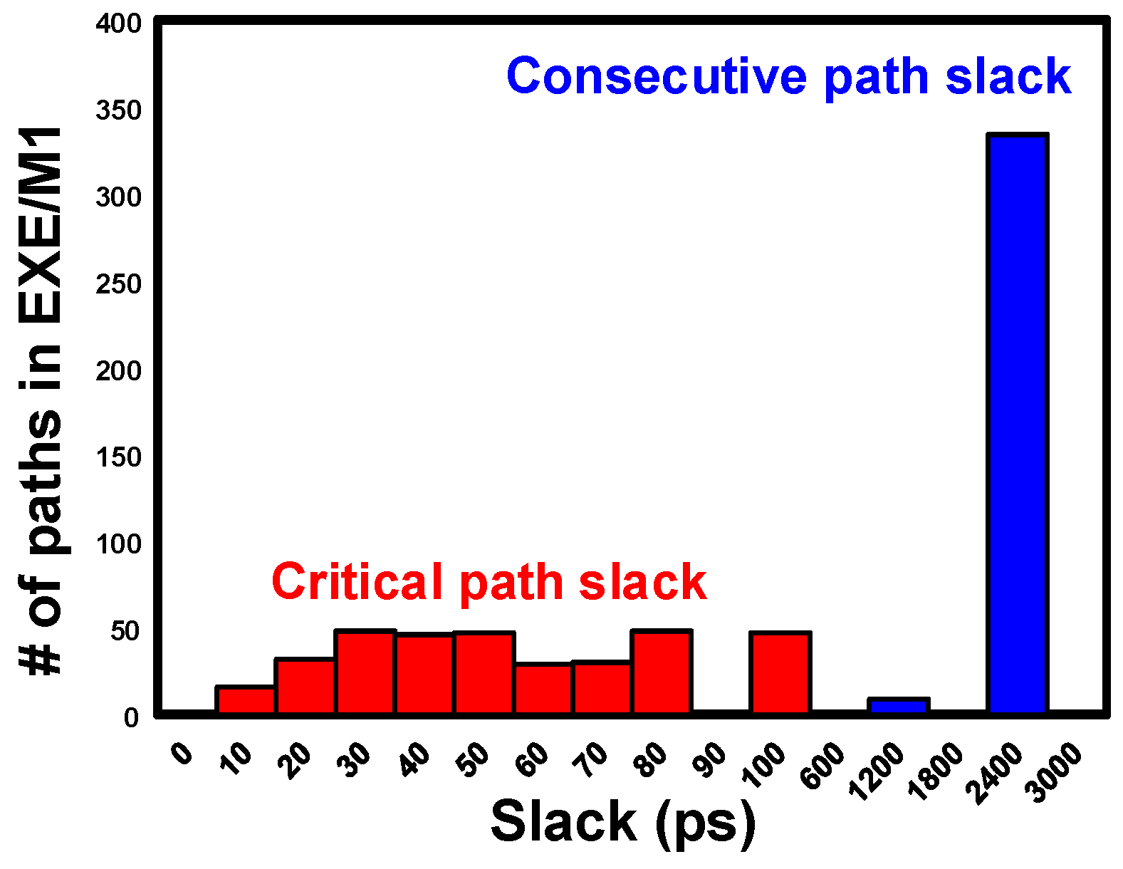
3.1. Slack Balancing
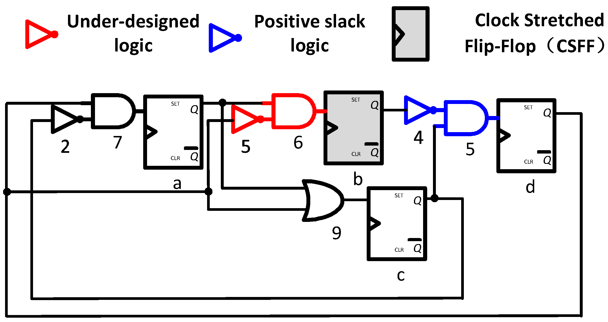
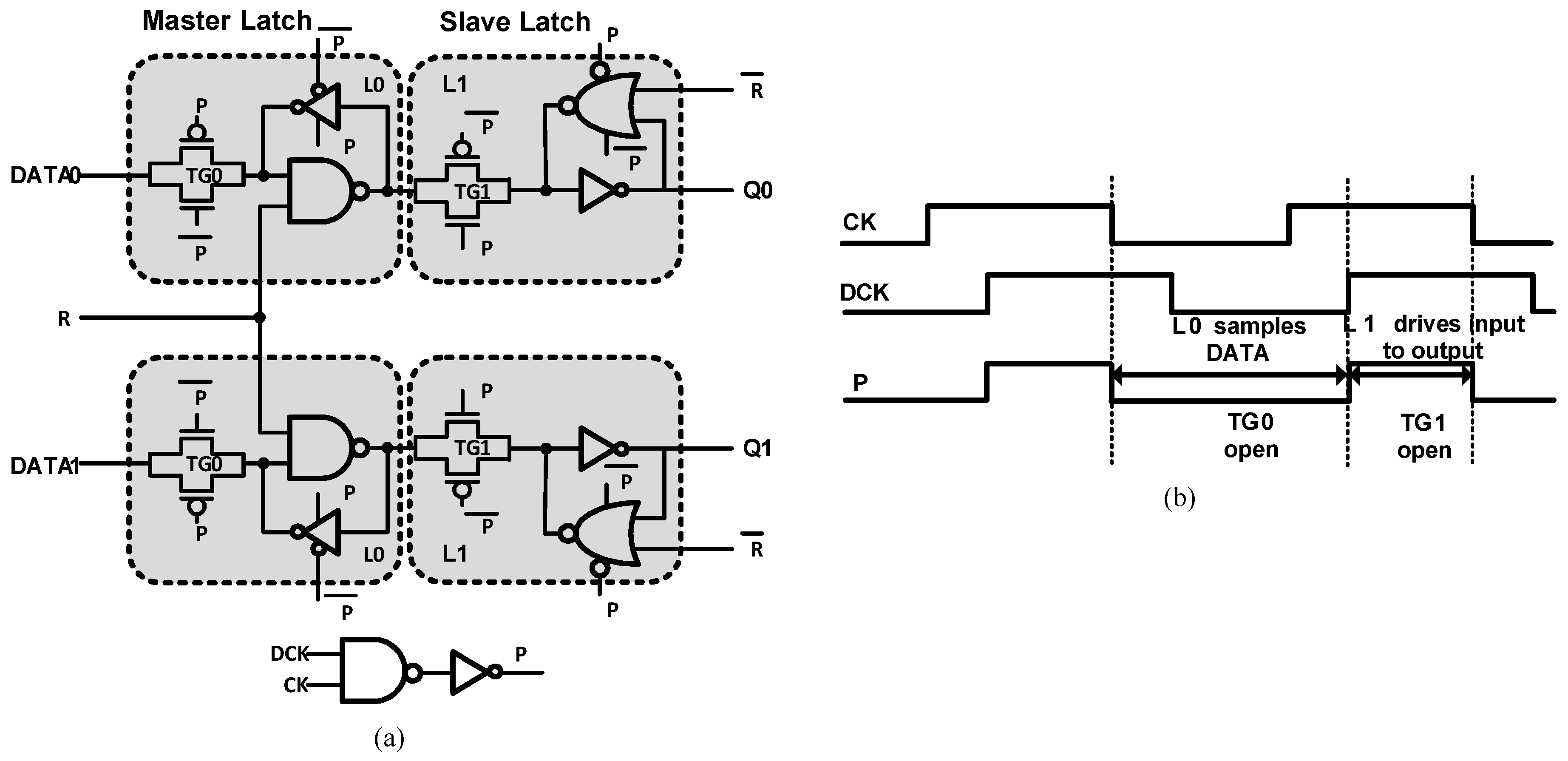
3.2. Clock Stretched Flip-Flop (CSFF)
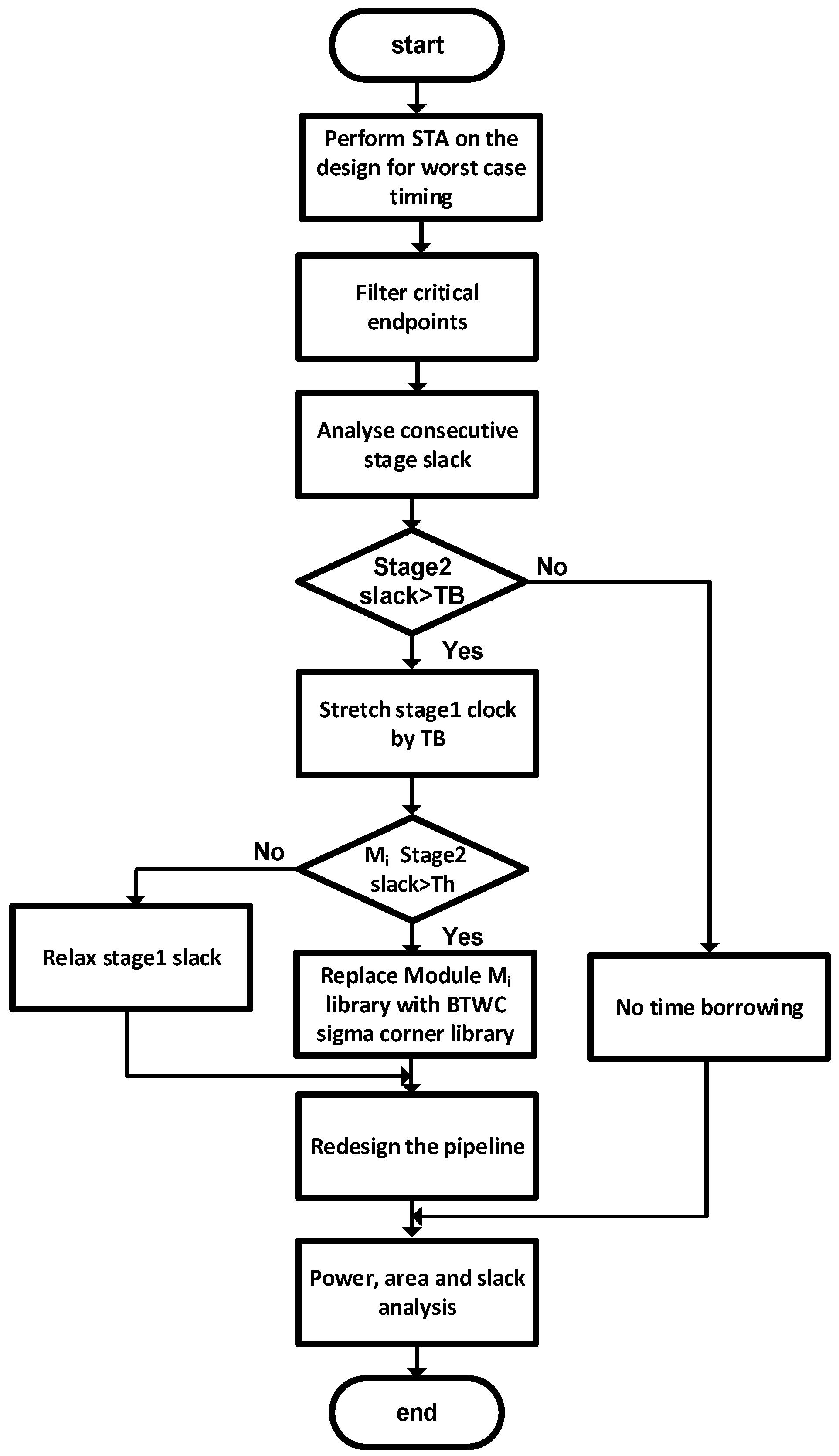
3.3. Design Flow
4. Power Optimization Algorithm
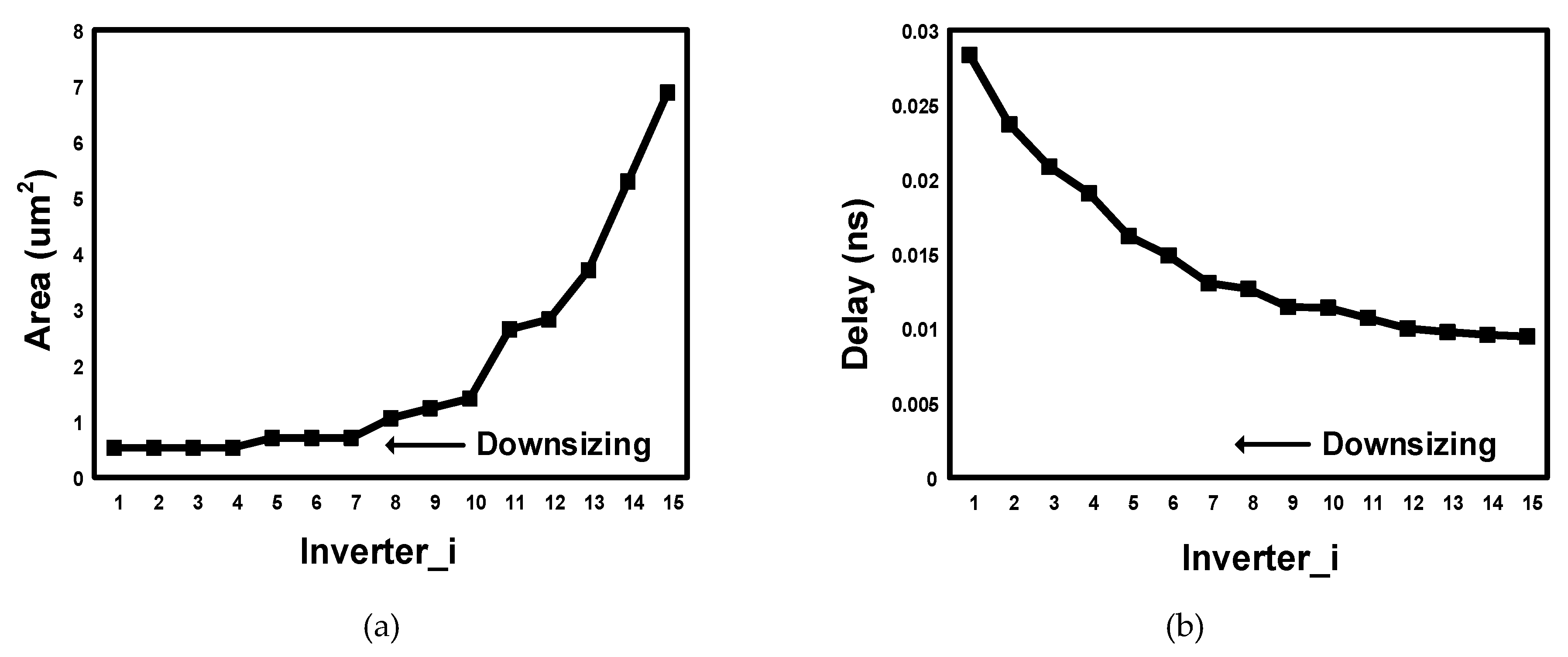
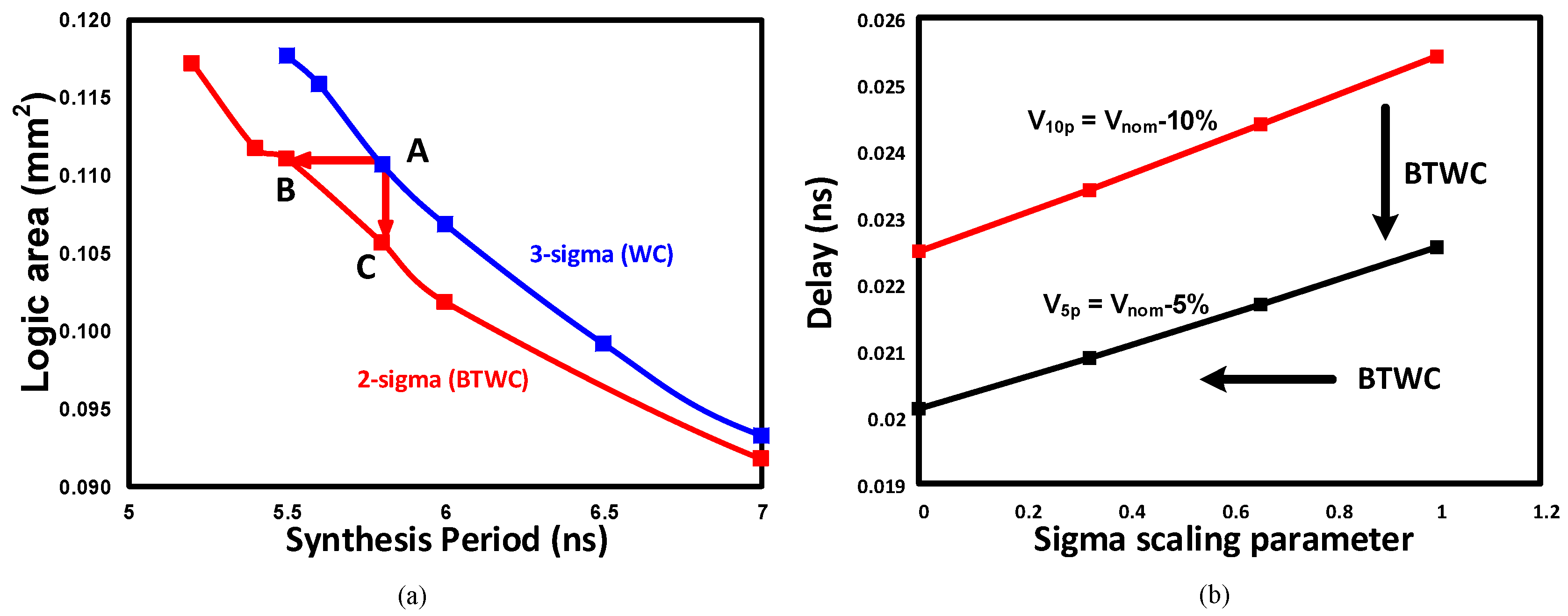
4.1. Power Optimization by Logic Reshaping (SizeOpt)
| Algorithm 1. Slack analysis & Downsizing (SizeOpt) |
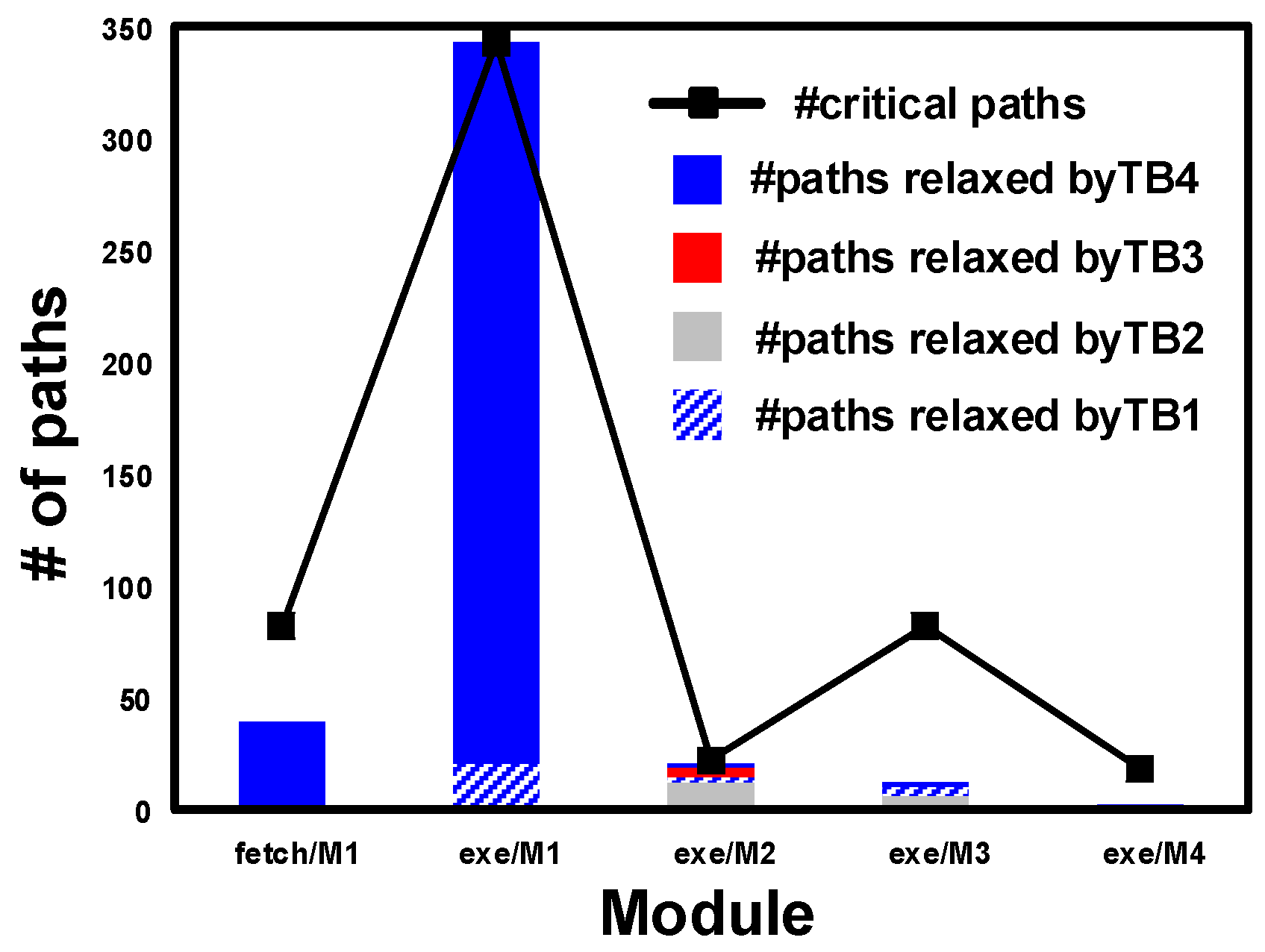
| 1. ProcedureSizeOpt (Initial Netlist) 2. Run STA to find critical paths P and consecutive slacks 3. P ← Φ 4. for all timing endpoints p in the netlist do 5. if slack(p) < Th then 6. P ← P U {p} 7. end if 8. end for 9. for all TB = TB4, TB >= TB1, TB = TB − TB1 do 10. for all p ∈ P do 11. if consecutive slack (p) >= TB and < 2TB then 12. Replace register CLK with stretched CLK, with DCK = TB 13. Relax fan-in logic timing by TB 14. end if 15. end for 16. end for 17. Redesign the pipeline and close timing 18. Calculate Power and Area savings 19. return (netlist) |
4.2. Power Optimization by Library Tuning (SigmaOpt)
| Algorithm 2. BTWC sigma library cell swap (SigmaOpt) |
| 1. ProcedureSigmaOpt (Initial Netlist) 2. Run STA to find critical paths P and consecutive slacks 3. P ← Φ 4. for all timing endpoints p in the netlist do 5. if slack(p) < Th then 6. P ← P U {p} 7. end if 8. end for 9. for all sigma = 0, sigma <= 2, sigma = sigma + 1 do 10. for all I = 0, i <= m, i = i + 1 do 11. if module Mi consecutive slack (Pi) >= TB then 12. Replace register CLK with stretched CLK, with DCK = TB 13. Swap the logic library with sigma library 14. end if 15. end for 16. Redesign the pipeline and close timing 17. Calculate Power and Area savings 18. return (netlistsigma) 19. end for |
5. Results and Analysis
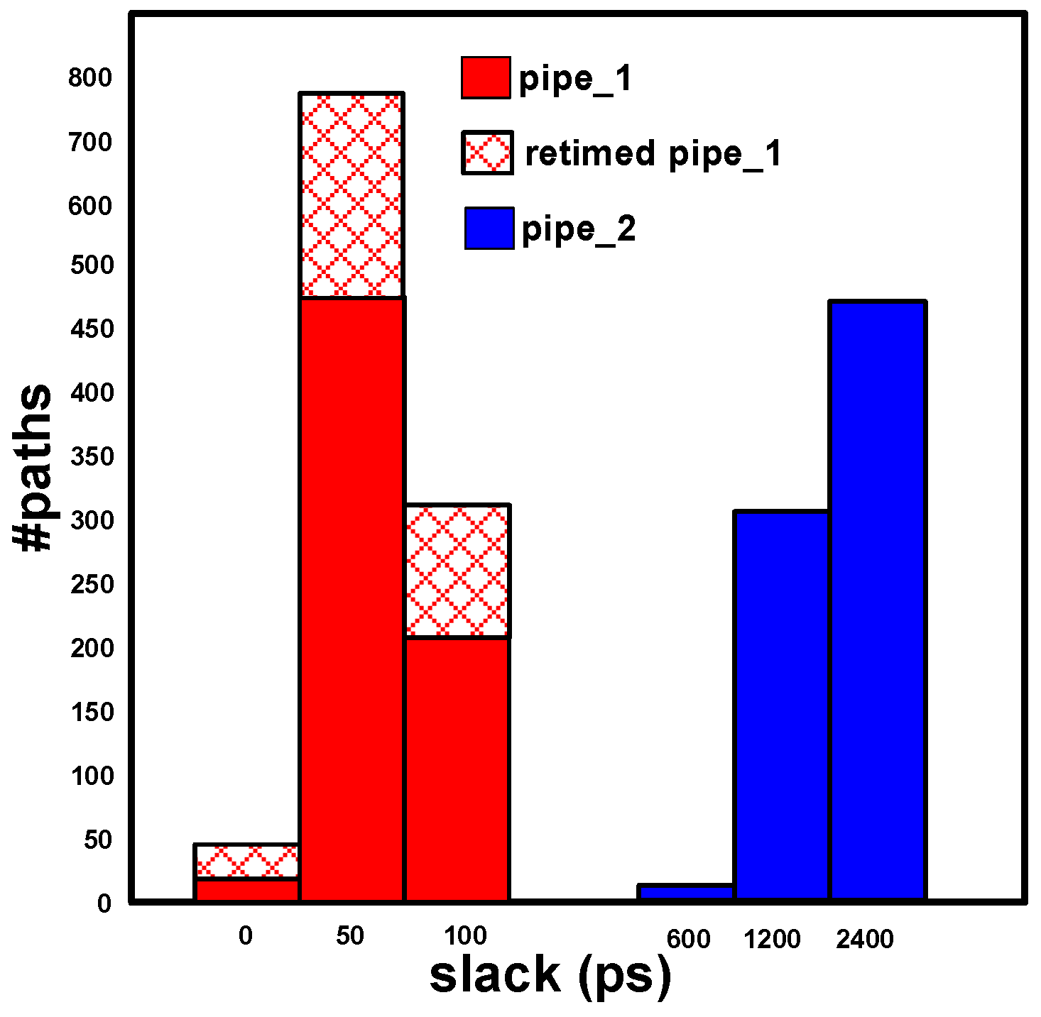
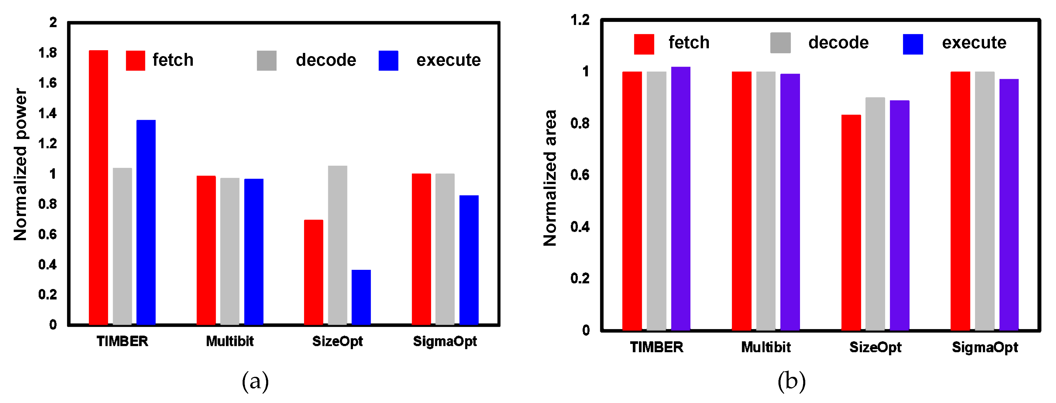
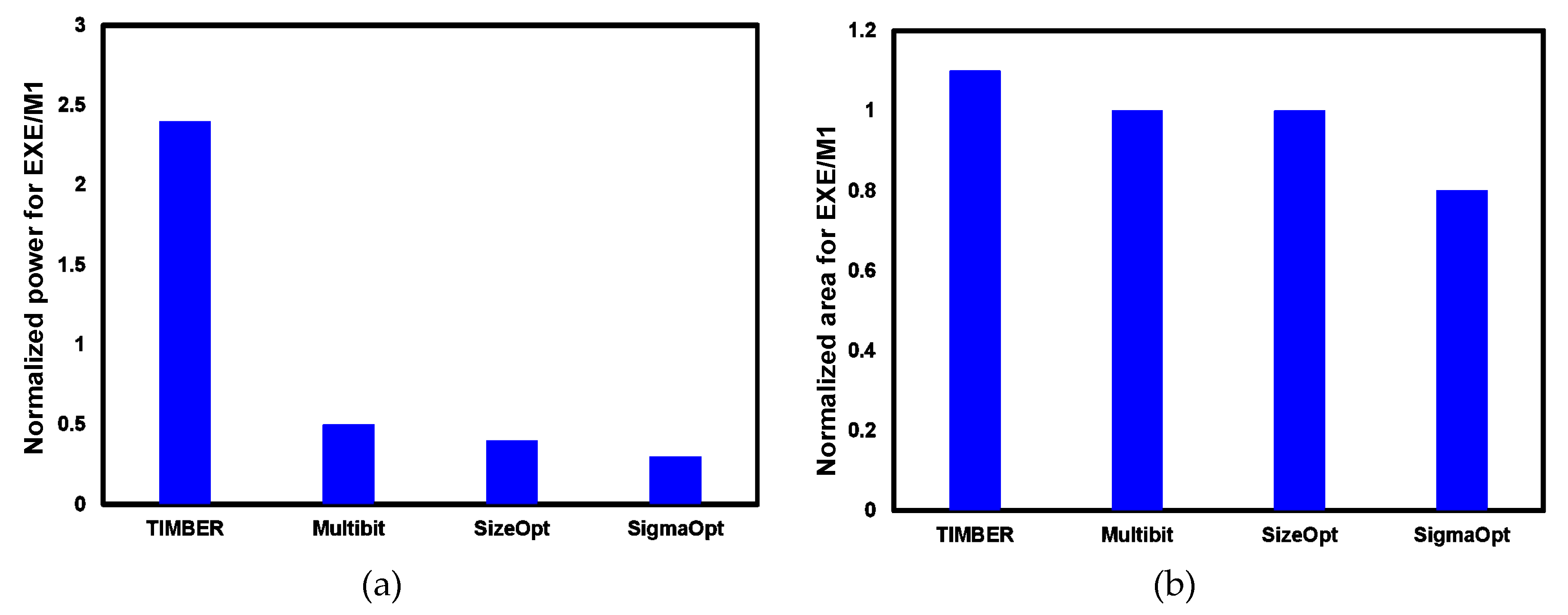
5.1. Flip-Flop Level Savings
5.2. Chip-Level Savings
6. Conclusions
Author Contributions
Funding
Acknowledgments
Conflicts of Interest
References
- Borkar, S.; Karnik, T.; Narendra, S.; Tschanz, J.; Keshavarzi, A.; De, V. Parameter Variations and Impact on Circuits and Microarchitecture. In Proceedings of the 40th Annual Design Automation Conference, Anaheim, CA, USA, 2–6 June 2003; pp. 338–342. [Google Scholar]
- Ghosh, S.; Roy, K. Parameter variation tolerance and error resiliency: New design paradigm for the nanoscale era. Proc. IEEE 2010, 8, 1718–1751. [Google Scholar] [CrossRef]
- Asenov, A.; Brown, A.R.; Davies, J.H.; Kaya, S.; Slavcheva, G. Simulation of intrinsic parameter fluctuations in deca-nanometer and nanometer-scale MOSFETs. IEEE Trans. Electron Devices 2003, 50, 1837–1852. [Google Scholar] [CrossRef]
- Nassif, S.R. Modeling and analysis of manufacturing variations. In Proceedings of the IEEE 2001 Custom Integrated Circuits Conference, San Diego, CA, USA, 9 May 2001; pp. 223–228. [Google Scholar]
- Borkar, S. Designing Reliable Systems from Unreliable Components: The Challenges of Transistor Variability and Degradation. IEEE Micro 2005, 25, 10–16. [Google Scholar] [CrossRef]
- Bowman, K.A.; Duvall, S.G.; Meindl, J.D. Impact of Die-to-Die and Within-Die Parameter Fluctuations on the Maximum Clock Frequency Distribution for Gigascale Integration. IEEE J. Solid State Circuits 2002, 37, 183–190. [Google Scholar] [CrossRef]
- Ronald, G.; Wieckowski, M.; Blaauw, D.; Sylvester, D.; Mudge, T. Near-Threshold Computing: Reclaiming Moore’s Law through Energy Efficient Integrated Circuits. Proc. IEEE 2010, 98, 253–266. [Google Scholar]
- Meijer, M.; Liu, B.; van Veen, R.; de Gyvez, J.P. Post-Silicon Tuning Capabilities of 45nm Low-Power CMOS Digital Circuits. In Proceedings of the Symposium on VLSI Circuits, Kyoto, Japan, 16–18 June 2009; pp. 110–111. [Google Scholar]
- Kim, T.; Persaud, R.; Kim, C.H. Silicon odometer: An on-chip reliability monitor for measuring frequency degradation of digital circuits. In Proceedings of the Very Large Scale Integrated (VLSI) Circuits Symposium, Tlanta, GA, USA, 15–17 October 2007; pp. 122–123. [Google Scholar]
- Gupta, P.; Agarwal, Y.; Dolecek, L.; Dutt, N.; Gupta, R.K.; Kumar, R.; Mitra, S.; Nicolau, A.; Rosing, T.S.; Srivastava, M.B.; et al. Underdesigned and Opportunistic Computing in Presence of Hardware Variability. IEEE Trans. Comput.-Aided Des. Integr. Circuits Syst. 2013, 32, 8–23. [Google Scholar] [CrossRef]
- Tschanz, J.; Bowman, K.; Walstra, S.; Agostinelli, M.; Karnik, T.; De, V. Tunable Replica Circuits and Adaptive Voltage-Frequency Techniques for Dynamic Voltage, Temperature and Aging Variation Tolerance. In Proceedings of the Symposium on VLSI Circuits, Kyoto, Japan, 16–18 June 2009; pp. 112–113. [Google Scholar]
- Ernst, D.; Kim, N.S.; Das, S.; Pant, S.; Rao, R.; Pham, T.; Ziesler, C.; Blaauw, D.; Austin, T.; Mudge, T.; et al. Razor: A Low-Power Pipeline Based on Circuit-Level Timing Speculation. In Proceedings of the 36th Symposium on Microarchitecture (MICRO-36), San Diego, CA, USA, 3–5 December 2003. [Google Scholar]
- Das, S.; Tokunaga, C.; Pant, S.; Ma, W.; Kalaiselvan, S.; Lai, K.; Bull, D.; Blaauw, D. Razor II: In Situ Error Detection and Correction for PVT and SER Tolerance. IEEE J. Solid-State Circuits 2009, 44, 32–48. [Google Scholar] [CrossRef]
- Bowman, K.; Tschanz, J.; Kim, N.; Lee, J.; Wilkerson, C.; Lu, S.; Karnik, T.; De, V. Energy-Efficient and Metastability-Immune Resilient Circuits for Dynamic Variation Tolerance. IEEE J. Solid-State Circuits 2009, 44, 49–63. [Google Scholar] [CrossRef]
- Fojtik, M.; Fick, D.; Kim, Y.; Pinckney, N.; Harris, D.M.; Blaauw, D.; Sylvester, D. Bubble Razor: Eliminating timing margins in an ARM cortex-M3 processor in 45 nm CMOS using architecturally independent error detection and correction. IEEE J. Solid-State Circuits 2013, 48, 66–81. [Google Scholar] [CrossRef]
- Joshi, V.; Blaauw, D.; Sylvester, D. Soft-edge flip-flops for improved timing yield: Design and optimization. In Proceedings of the IEEE/ACM International Conference on Computer-Aided Design, San Jose, CA, USA, 5–8 November 2007; pp. 667–673. [Google Scholar]
- Choudhury, M.; Chandra, V.; Mohanram, K.; Aitken, R. TIMBER: Time borrowing and error relaying for online timing error resilience. In Proceedings of the DATE, Dresden, Germany, 8–12 March 2010; pp. 1554–1559. [Google Scholar]
- Bull, D.; Das, S.; Shivashankar, K.; Dasika, G.; Flautner, K.; Blaauw, D. A power-efficient 32 bit ARM processor using timing-error detection and correction for transient-error tolerance and adaptation to PVT variation. IEEE J. Solid-State Circuits 2011, 46, 18–31. [Google Scholar] [CrossRef]
- Das, S.; Roberts, D.; Lee, S.; Pant, S.; Blaauw, D.; Austin, T.; Flautner, K.; Mudge, T.T. A self-tuning DVS processor using delay error detection and correction. IEEE J. Solid-State Circuits 2006, 41, 792–804. [Google Scholar] [CrossRef]
- Austin, T.; Bertacco, V.; Blaauw, D.; Mudge, T. Opportunities and Challenges for Better Than Worst-Case Design. In Proceedings of the Asia and South Pacific Design Automation Conference, Shanghai, China, 18–21 January 2005; pp. 2–7. [Google Scholar]
- Moreno, S.; de Gyvez, J.P. A better than worst case circuit design using timing-error speculation and frequency adaptation. In Proceedings of the IEEE International SOC Conference, Niagara Falls, NY, USA, 12–14 September 2012; pp. 15–20. [Google Scholar]
- Kahng, A.B.; Kang, S.; Kumar, R.; Sartori, J. Slack Redistribution for Graceful Degradation Under Voltage Overscaling. In Proceedings of the 15th Asia and South Pacific Design Automation Conference (ASP-DAC), Taipei, Taiwan, 18–21 January 2010; pp. 825–831. [Google Scholar]
- Sarangi, S.R.; Greskamp, B.; Tiwari, A.; Torrellas, J. EVAL: Utilizing processors with variation-induced timing errors. In Proceedings of the International Symposium on Microarchitecture, Lake Como, Italy, 8–12 November 2008. [Google Scholar]
- Greskamp, B.; Wan, L.; Karpuzcu, W.R.; Cook, J.J.; Torrellas, J.; Chen, D.; Zilles, C. BlueShift: Designing Processors for Timing Speculation from the Ground Up. In Proceedings of the IEEE International Symposium on High Performance Computer Architecture, Raleigh, NC, USA, 14–18 February 2009; pp. 213–224. [Google Scholar]
- Kahng, A.B.; Kang, S.; Kumar, R.; Sartori, J. Designing a Processor from the Ground Up to Allow Voltage/Reliability Tradeoffs. In Proceedings of the IEEE International Symposimum on High-Performance Computer Architecture, Bangalore, India, 9–14 January 2010. [Google Scholar]
- Kahng, A.B.; Kang, S.; Li, J. A New Methodology for Reduced Cost of Resilience. In Proceedings of the GLSVLSI, Houston, TX, USA, 21–23 May 2014; pp. 157–162. [Google Scholar]
- Jayakrishnan, M.; Chang, A.; Kim, T. Power and Area Efficient Clock Stretching and Critical Path Reshaping for Error Resilience. In Proceedings of the IFIP/IEEE International Conference on Very Large Scale Integration (VLSI-SoC), Tallinn, Estonia, 26–28 September 2016. [Google Scholar]
- Jayakrishnan, M.; Chang, A.; Kim, T. Library Pruning and Sigma Corner Libraries for Power Efficient Variation Tolerant Processor Pipelines. In Proceedings of the IFIP/IEEE International Conference on Very Large Scale Integration (VLSI-SoC), Abu Dhabi, UAE, 23–25 October 2017. [Google Scholar]
- Jayakrishnan, M.; Chang, A.; Kim, T. Opportunistic Design Margining for Area and Power Efficient Processor Pipelines in Real Time Applications. J. Low Power Electron. Appl. 2018, 8, 9. [Google Scholar] [CrossRef]


| Feature | Design Level Optimization | Sequential Optimization Based on Error Detection | Combinational & Sequential Optimization | Sequential Optimization Based on Error Masking | Proposed |
|---|---|---|---|---|---|
| Speculation Mechanism | ABB, ASV, OSB, PCT | Adaptive voltage/frequency scaling | Adaptive voltage/frequency scaling | Adaptive voltage/frequency scaling | Non-speculative, based on cell downsizing and BTWC library |
| Error Handling | Duplicate paths | Duplicate Latch/FFs | Duplicate Latch/FFs | Duplicate Latch/FFs | No error |
| Clock Tree Loading | No | Yes | Yes | Yes | No |
| Short Path Padding | No | Yes | Yes | Yes | Yes |
| Sequential Overhead | Large | Large | Large | Large | None |
| Combinational Overhead | Small | Small | Small | Small | None |
| Meta-stability | Yes | Yes | Yes | Yes | No |
| Techniques | EVAL, Blueshift | Razor I, Razor II, Bubble Razor DSTB, TDTB | Slack Optimizer, Skew Optimizer, CombOpt | TIMBER, soft edge flip-flop | Clock stretched flip-flop |
| Variables | TIMBER FF | Proposed |
|---|---|---|
| C to Q delay rising | 91.62ps | 77.5ps |
| C to Q delay falling | 91.83ps | 80.67ps |
| Max power@ 1.1V | 3.21uW | 2.608uW |
| Min Power@1.1V | 1.857uW | 1.478uW |
| Power (µW) | Baseline | TIMBER | Multibit | SizeOpt | SigmaOpt | ||||||||||
|---|---|---|---|---|---|---|---|---|---|---|---|---|---|---|---|
| Leakage | Dynamic | Total | Leakage | Dynamic | Total | Leakage | Dynamic | Total | Leakage | Dynamic | Total | Leakage | Dynamic | Total | |
| Fetch | 1.5 | 265.1 | 266.6 | 1.5 | 482.4 | 483.9 | 1.5 | 261.2 | 262.7 | 1.1 | 184 | 185.1 | 1.5 | 265.1 | 266.6 |
| Dec. | 0.9 | 149.1 | 150 | 0.8 | 154.8 | 155.6 | 0.9 | 144.9 | 145.8 | 0.7 | 157.3 | 158 | 0.9 | 149.1 | 150 |
| Exe. | 14.8 | 1307.9 | 1322.7 | 14.7 | 1777.4 | 1792.2 | 14.8 | 1262.2 | 1277 | 11.2 | 471.7 | 482.9 | 15.5 | 1118.6 | 1134.1 |
| Area (mm2) | Baseline | TIMBER | Multibit | SizeOpt | SigmaOpt | |||||||||||||||
|---|---|---|---|---|---|---|---|---|---|---|---|---|---|---|---|---|---|---|---|---|
| #Cells | Cell | Net | Total | #Cells | Cell | Net | Total | #Cells | Cell | Net | Total | #Cells | Cell | Net | Total | #Cells | Cell | Net | Total | |
| Fetch | 1976 | 0.005 | 0.007 | 0.012 | 2014 | 0.005 | 0.007 | 0.012 | 1920 | 0.005 | 0.007 | 0.012 | 1751 | 0.004 | 0.006 | 0.01 | 1976 | 0.005 | 0.007 | 0.012 |
| Dec. | 1874 | 0.003 | 0.007 | 0.01 | 1900 | 0.003 | 0.007 | 0.01 | 1867 | 0.003 | 0.007 | 0.01 | 1796 | 0.003 | 0.006 | 0.009 | 1874 | 0.003 | 0.007 | 0.01 |
| Exe. | 16414 | 0.045 | 0.063 | 0.108 | 16356 | 0.047 | 0.063 | 0.11 | 15964 | 0.045 | 0.062 | 0.107 | 15053 | 0.038 | 0.058 | 0.096 | 15734 | 0.043 | 0.061 | 0.105 |
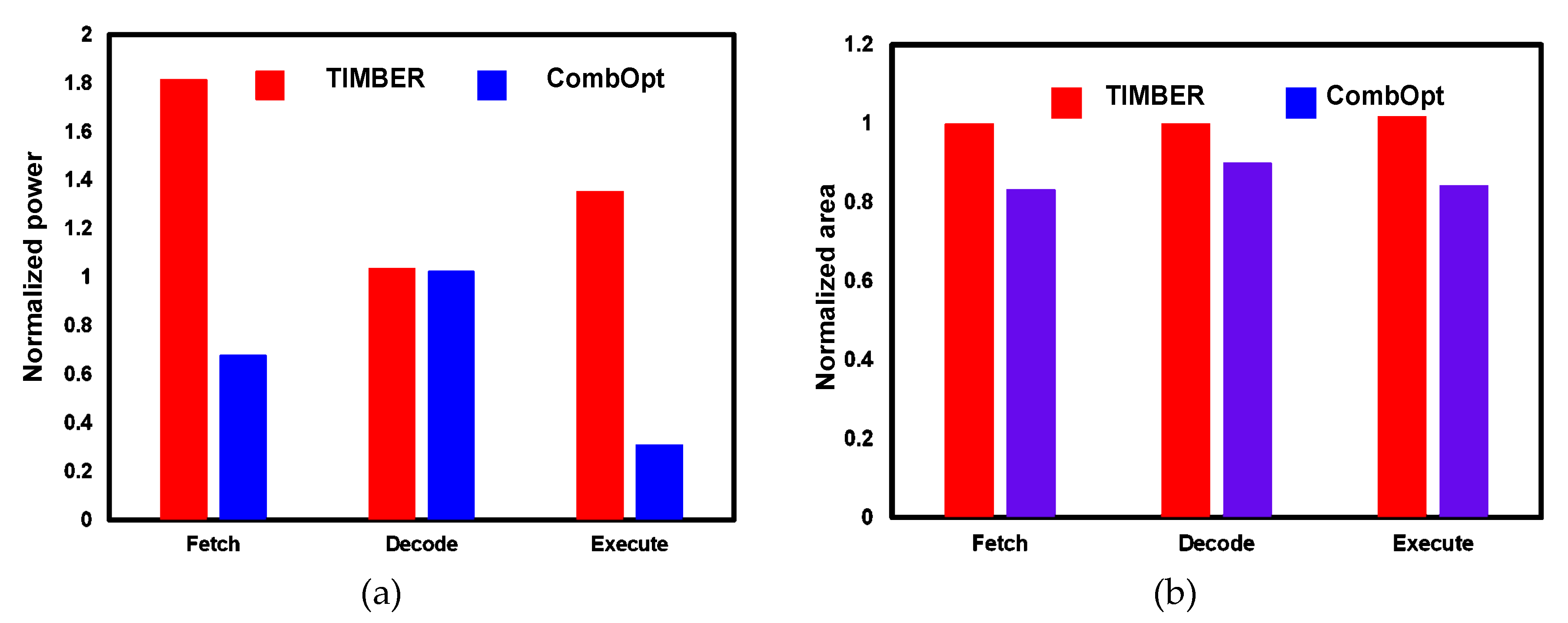
| Power (µW) | Baseline | TIMBER | CombOpt | |||||||||
|---|---|---|---|---|---|---|---|---|---|---|---|---|
| # of Cells | Leakage | Dynamic | Total | # of Cells | Leakage | Dynamic | Total | # of Cells | Leakage | Dynamic | Total | |
| Fetch | 1976 | 1.5 | 265.1 | 266.6 | 2014 | 1.5 | 482.4 | 483.9 | 1695 | 1.1 | 180.1 | 181.2 |
| Dec. | 1874 | 0.9 | 149.1 | 150 | 1900 | 0.8 | 154.8 | 155.6 | 1789 | 0.7 | 153.1 | 153.8 |
| Exe. | 16414 | 14.8 | 1307.9 | 1322.7 | 16356 | 14.7 | 1777.4 | 1792.2 | 14012 | 11.968 | 396.947 | 408.915 |
| Area (mm2) | Baseline | TIMBER | CombOpt | |||||||||
|---|---|---|---|---|---|---|---|---|---|---|---|---|
| # of Cells | Cell Area | Net Area | Total | # of Cells | Cell Area | Net Area | Total | # of Cells | Cell Area | Net Area | Total | |
| Fetch | 1976 | 0.005 | 0.007 | 0.012 | 2014 | 0.005 | 0.007 | 0.012 | 1695 | 0.004 | 0.006 | 0.01 |
| Dec. | 1874 | 0.003 | 0.007 | 0.01 | 1900 | 0.003 | 0.007 | 0.01 | 1789 | 0.003 | 0.006 | 0.009 |
| Exe. | 16414 | 0.045 | 0.063 | 0.108 | 16356 | 0.047 | 0.063 | 0.11 | 14012 | 0.035 | 0.056 | 0.091 |
© 2019 by the authors. Licensee MDPI, Basel, Switzerland. This article is an open access article distributed under the terms and conditions of the Creative Commons Attribution (CC BY) license (http://creativecommons.org/licenses/by/4.0/).
Share and Cite
Jayakrishnan, M.; Chang, A.; Kim, T.T.-H. Power and Area Efficient Clock Stretching and Critical Path Reshaping for Error Resilience. J. Low Power Electron. Appl. 2019, 9, 5. https://doi.org/10.3390/jlpea9010005
Jayakrishnan M, Chang A, Kim TT-H. Power and Area Efficient Clock Stretching and Critical Path Reshaping for Error Resilience. Journal of Low Power Electronics and Applications. 2019; 9(1):5. https://doi.org/10.3390/jlpea9010005
Chicago/Turabian StyleJayakrishnan, Mini, Alan Chang, and Tony Tae-Hyoung Kim. 2019. "Power and Area Efficient Clock Stretching and Critical Path Reshaping for Error Resilience" Journal of Low Power Electronics and Applications 9, no. 1: 5. https://doi.org/10.3390/jlpea9010005
APA StyleJayakrishnan, M., Chang, A., & Kim, T. T.-H. (2019). Power and Area Efficient Clock Stretching and Critical Path Reshaping for Error Resilience. Journal of Low Power Electronics and Applications, 9(1), 5. https://doi.org/10.3390/jlpea9010005