Abstract
The ongoing revolution in Deep Learning is redefining the nature of computing that is driven by the increasing amount of pattern classification and cognitive tasks. Specialized digital hardware for deep learning still holds its predominance due to the flexibility offered by the software implementation and maturity of algorithms. However, it is being increasingly desired that cognitive computing occurs at the edge, i.e., on hand-held devices that are energy constrained, which is energy prohibitive when employing digital von Neumann architectures. Recent explorations in digital neuromorphic hardware have shown promise, but offer low neurosynaptic density needed for scaling to applications such as intelligent cognitive assistants (ICA). Large-scale integration of nanoscale emerging memory devices with Complementary Metal Oxide Semiconductor (CMOS) mixed-signal integrated circuits can herald a new generation of Neuromorphic computers that will transcend the von Neumann bottleneck for cognitive computing tasks. Such hybrid Neuromorphic System-on-a-chip (NeuSoC) architectures promise machine learning capability at chip-scale form factor, and several orders of magnitude improvement in energy efficiency. Practical demonstration of such architectures has been limited as performance of emerging memory devices falls short of the expected behavior from the idealized memristor-based analog synapses, or weights, and novel machine learning algorithms are needed to take advantage of the device behavior. In this article, we review the challenges involved and present a pathway to realize large-scale mixed-signal NeuSoCs, from device arrays and circuits to spike-based deep learning algorithms with ‘brain-like’ energy-efficiency.
1. Introduction
A recent grand challenge in semiconductor technology urges researchers to “Create a new type of computer that can proactively interpret and learn from data, solve unfamiliar problems using what it has learned, and operate with the energy efficiency of the human brain [1].” Artificial Intelligence (AI) techniques such as deep neural networks, or deep learning, have found widespread success when applied to several problems including image and video interpretation, speech and natural language processing, and medical diagnostics [2]. At present, much of cognitive computing is performed on digital graphics processing units (GPUs), accelerator application-specific integrated circuits (ASICs), or field-programmable gate arrays (FPGAs), mostly at the data center end of the Cloud infrastructure. However, the current explosion in widespread deployment of deep-learning applications is expected to hit a power-performance wall with—(1) plateauing in Complementary Metal Oxide Semiconductor (CMOS) scaling, and (2) limits set for energy consumption in the Cloud. These deep learning implementations take long computing cluster days to train a network for realistic applications. Even with remarkable progress made in computing, the agile human brain provides an existential proof that learning can be more sophisticated while allowing compactness and energy-efficiency. Furthermore, there is a growing interest in edge computing and intelligent cognitive assistants (ICAs), where deep learning and/or inference will be available on energy-constrained mobile platforms, autonomous drones, and internet-of-things sensor nodes, which not only eliminate the reliance on cloud-based AI service, but also ensure privacy of user data.
In contrast to the predominant von Neumann computers where memory and computing elements are separated, a biological brain retains memories and performs ‘computing’ using largely homogeneous neural motifs. In a brain, neurons perform computation by propagating spikes and storing memories in the relative strengths of synapses, and by forming new connections (or morphogenesis) [3]. By repeating these simple cortical columnar organization of neurons and synapses, a biological brain realizes a highly energy-efficient cognitive computing motif. Inspired by biological nervous systems, artificial neural networks (ANNs) were developed that have achieved remarkable success in a few specific applications. In the past decade, by leveraging parallel GPUs, ASICs [4], or FPGAs, power consumption of artificial neural networks has been reduced but yet remains significantly higher than their biological counterpart developed through millions of years of evolution. The discovery of spike-timing-dependent-plasticity (STDP) local learning rule [5,6] and mathematical analysis of spike-based winner-take-all (WTA) motifs have opened new avenues in spike-based neural network research. Recent studies have suggested that STDP, and its neural-inspired variants, can be used to train spiking neural networks (SNNs) in situ without trading off their parallelism [7,8].
The current-art in neuromorphic computing has been recently reviewed with focus on the device aspects [9] or high-level system architectures [10,11]. The unique contribution of this review article is the focus on the interfacing of mixed-signal circuits with emerging synaptic devices and discussion on the resulting design considerations that impact the overall energy-efficiency and scalability of large-scale NeuSoCs. In addition, a survey of recent learning algorithms and their associated challenges is presented for the realizing of deep learning in NeuSoCs. This article is organized as follows. Section 2 presents an overview of existing neuromorphic computing platforms and the potential for employing nanoscale emerging memory devices. Section 3 presents a review on mixed-signal approaches to neuromorphic computing leveraging crossbar arrays of emerging memory devices and details on neural circuits and learning algorithms followed by challenges associated with emerging memory devices. Section 4 makes an argument for bio-plausible dendritic processing using compound stochastic synapses. Section 5 discusses energy-efficiency implications of device properties on neuromorphic SoCs. Section 6 presents the direction for algorithm development for large-scale deep learning using neurmorphic substrates followed by conclusions.
2. Neuromorphic Computing and Emerging Devices
2.1. Digital Neuromorphic Platforms
Recent progress in neuromorphic hardware has led to development of asynchronous event-driven, as opposed to synchronous or clock-driven, integrated circuits (ICs) that process and communicate information using spatio-temporal voltage spike signals. Most pertinent examples of a digital neuromorphic hardware are IBM’s TrueNorth [12], SpiNNaker system from the Human Brain Project and the University of Manchester (Manchester, UK) [13], and recently Loihi chip from Intel (Hillsboro, OR, USA) [14]. IBM’s (San Jose, CA, USA) TrueNorth ASIC comprises of 4096 cores, with 1 million programmable neurons and 256 million programmable synapses as communication channels between the digital neurons, and consumes ≈100 mW for pattern classification tasks [12]. However, the networks are trained offline as the chip does not allow in situ learning. On the other hand, Intel’s Loihi ASIC implements on-chip learning with flexibility in neuron and synapse behavior, but trades off learning with reduced neurosynaptic density [14]. Purely digital implementations have low neurosynaptic density and large die area that can limit the scalability and cost of the resulting neuromorphic systems. Furthermore, leakage power in static random access memory (SRAM)-based digital synapses can limit the overall energy-efficiency.
2.2. Subthreshold Analog Neuromorphic Platforms
Advances in analog neuromorphic circuits include subthreshold bio-mimetic CMOS circuits that were developed to reproduce ion-channel dynamics occurring in biological neural networks [15]. These implementations leveraged the fact that the brain performs analog-like spike-based computation with a massive number of imprecise components. However, the fundamental limitation of such architectures was that the weights were dynamically stored and updated on capacitors, which leak away in a few milliseconds, limiting any long-term learning [16,17]. Bistability of analog weights has been used as an intermittent solution for long-term storage of weights [16,18,19,20,21,22,23,24]. However, recent studies on deep SNNs have determined that at least 4-bit resolution is needed for the synaptic weights to attain classification accuracy comparable to conventional deep learning [25,26]. Storing the weights digitally and converting them to analog synapses using a Digital-to-Analog Converter (DAC) is also a possibility and has been implemented on wafer-scale hardware in [27,28]. However, such architectures, even though extremely beneficial for neuroscience research, preclude high synaptic density envisioned for NeuSoCs.
2.3. Neuromorphic Platforms Using Floating-Gate and Phase Change Memories
Other solutions include using non-volatile memories (NVMs) such as the floating gate (or Flash memory) devices [29,30] and phase change memory (PCM) [9,31] for implementing synaptic weights. The endurance of floating-gate devices is typically 100–500k cycles due to the high voltages used for program and erase operations [32]. This will preclude on-chip training of neural networks where millions of program/erase operations need to be supported. Flash memory is best suited for low-power inference applications [33] or for scenarios where learning concludes within the endurance limit of the devices. Recently, IBM’s neuromorphic group has shown encouraging results by employing PCM devices employed as synapses in SNNs [9,34]. PCM devices can provide incremental states in the program direction by controlling the amount of crystallization on the memory cell. However, the erase can be abrupt as the device undergoes a melt-and-quench phase when brought to the amorphous state [9,35].
2.4. Nanoscale Emerging Devices
In the last decade, there has been a renewed interest in two-terminal resistive memory devices, including the elusive memristor, as these resistive random access memory (RRAM), Mott memory [36], and similar devices promise very high memory density (/cm) [37,38]. These devices have demonstrated biologically plausible STDP plasticity behavior in several experiments [38,39] and therefore have emerged as an ideal candidate for realizing electronic equivalent of synapses. In addition, recent advances in these devices have shown low-energy consumption to change their states with sub-100fJ switching energy and very compact layout footprint ( nm pitch with cell size [40,41,42]. Following this trend, hybrid CMOS-RRAM analog very-large-scale integrated (VLSI) circuits have been proposed [43,44] to achieve dense integration of CMOS neurons with these emerging devices for neuromorphic computing chips by leveraging the contemporary nanometer silicon processing technology. Furthermore, three-terminal synaptic transistors based on liquid ion, lithium-ion and transition metal oxides have been reported and can be promising candidates for neuromorphic computing in the future [36,45,46].
The author also introduced a first compact CMOS memristor emulator circuit [47,48] and the resulting dynamic synapse circuits [24] but concluded that non-volatile synapses are needed for long-term retention of weights, high synaptic density and low leakage power in trained neural networks. Consequently, the Neuromorphic computing architecture development requires synergistic development in devices, circuits and learning algorithms to take advantage of the high synaptic density while not being oblivious to the challenges at the device-circuit interface. Following four necessary criterion have been identified for realizing large scale NeuSoCs capable of deep learning:
- Non-volatility and high-resolution of the synaptic weights
- High neurosynaptic density, approaching billions of synapses and millions of neurons per chip
- Massively-parallel learning algorithms with localized updates (or in-memory computing)
- Event-driven ultra-low-power neural computation and communication
3. Mixed-Signal Neuromorphic Architecture
Mixed-signal neuromorphic ICs promise the potential for embedded learning and pattern classification with orders of magnitude lower energy consumption than the von Neumann processors. As discussed in the previous section, this is feasible due to the densely-integrated non-volatile memory devices that include RRAM [49,50], phase-change random access memory (PCRAM), conductive-bridge random access memory (CBRAM) [51], Spin-Transfer Torque Random Access Memory (STTRAM) [52] and 3D crosspoint memory [53]. These are also referred to as memristors or memristive devices in literature [38,54].
3.1. Crossbar Networks
CMOS neurons and RRAM synapses are organized in a crossbar network to realize a single-level of neural interconnections as shown in Figure 1. In this architecture, each input neuron is connected to another output neuron through a two-terminal RRAM to form a crossbar, or cross-point, array. By cascading and/or stacking such crossbars, a deep neural network can be realized in hardware. Furthermore, maximum synaptic density is achieved by minimizing or eliminating the overheads associated with the synapse, while transferring the complexity to the peripheral neurons. The crossbar architecture is tolerant to sneak-paths in the array as all devices are concurrently used in the neural network, as opposed to the random access case where individual RRAM bit(s) are accessed and read out one at a time [55]. Consequently, the sneak paths are absorbed into the network weights with tolerable performance degradation. Furthermore, advanced packaging techniques such as through silicon via (TSV) for multiple chips and flip-chip integration can be leveraged to realize 3D stacking of such networks.
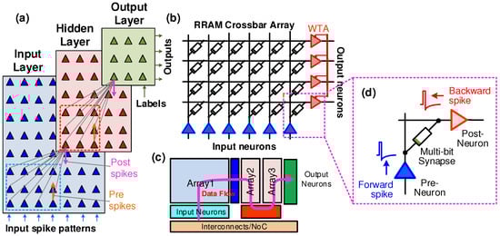
Figure 1.
Neuromorphic System-on-a-chip architecture (NeuSoC): (a) a fully-connected spiking neural network (SNN) showing input, hidden and output layers of spiking neurons. Here, synaptic connections shown for the input receptive field of a single neuron in the hidden and output layers; (b) a section of the neural network architecture implemented using resistive random access memory (RRAM) crossbar array and column/rows of mixed-signal complementary metal oxide semiconductor (CMOS) neurons; (c) a possible chip floorplan showing 2D arrays and peripheral circuits layout common in memory chips to build high-density SNN hardware. Scaling of NeuSoCs requires network-on-chip (NoC) and interconnect architecture for spatiotemporal data communication; (d) a single multi-bit synapse between the input (pre-synaptic) and output (post-synaptic) neurons that adjusts its weight using spike-timing dependent plasticity (STDP).
3.2. Analog Synapses Using RRAM/Memristors
Several nano-scale RRAM or memristors in literature have shown that their conductance modification characteristics are similar to the STDP rule from neurobiology [42,56,57] and thus are potentially an ideal candidate for implementing electronic synapses. STDP states that the synaptic weight w is updated according to the relative timing of the pre- and post-synaptic neuron firing. This is a form of Hebbian learning that postulates that “neurons that fire together, wire together [58].” As illustrated in Figure 2a, a spike pair with the pre-synaptic spike arrives before the post-synaptic spike results in increasing the synaptic strength, or long-term potentiation (LTP); a pre-synaptic spike after a post-synaptic spike results in decreasing the synaptic strength, or long-term depression (LTD). Changes in the synaptic weight plotted as a function of the relative arrival timing of the post-synaptic spike with respect to the pre-synaptic spike is called the STDP learning function or learning window. Furthermore, during the inference mode, only the pre-spikes with the positive rectangular pulse are used for carrying the feedforward inputs through the SNN. The post-spikes and the negative tails are activated during the training mode only to enable on-chip learning. This not only saves energy but also avoids undesirable changes to the synaptic weights [44,59].
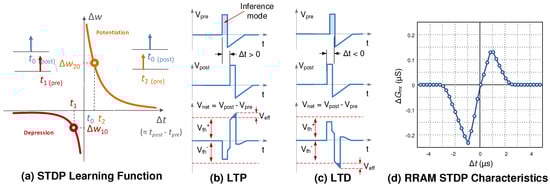
Figure 2.
Pairwise STDP with resistive random access memory (RRAM) devices: (a) graphical illustration of the pairwise STDP learning window with change in weight plotted as a function of time difference between the pre and post spikes. A spike pair creates net potential difference across the RRAM. (b) when , Long-term potentiation (LTP) occurs and RRAM conductance is increased (program operation). (c) For , LTD occurs and the RRAM conductance is decreased (erase operation). During the inference mode, only positive head of the pulse is enabled with amplitude so that the RRAM state is not disturbed; (d) simulated pairwise STDP learning window for modeled RRAM device. The change in conductance is around 1 s conductance with 5 s relative time range.
In pair-wise STDP learning, spikes sent from pre- and post-synaptic have their voltage amplitudes below the program and erase switching thresholds ( and ) of a bipolar RRAM device. RRAM switching events may occur only if this spike pair overlaps and creates a net potential () greater than the switching threshold, as illustrated in Figure 2b,c. Here, for , RRAM is incrementally programmed (conductance is increased) causing long-term potentiation (LTP) in the synapse. On the other hand, for the case , the RRAM is incrementally erased (conductance is decreased) and long-term depression (LTD) occurs in the synapse. In case of no temporal overlap, the pre-synaptic pulse is integrated in the neuron and thus should have a net positive area and smaller amplitude than the program or erase thresholds. This in turn sets a constraint for the voltage spikes that must always be ensured to avoid disturbing the RRAM state. This scheme effectively converts the time overlap () of pre and post spikes into program or erase voltage pulses [59,60,61,62]. During the inference (or read-only) mode, only positive head of the spike pulse is enabled with an amplitude so that the RRAM state is not inadvertently written. The simulated STDP learning window for an RRAM device modeled in [44] is shown in Figure 2d. For experimental pairwise STDP results from similar RRAM devices, the reader is referred to [35,38,56].
3.3. Event-Driven Neurons with Localized Learning
There is a significant body of work over the past several decades on low-power spiking neurons using subthreshold CMOS that are documented in [15] and references therein. However, driving thousands of resistive devices in parallel while maintaining desired energy-efficiency presents difficult challenges for CMOS neurons. This difficulty is further analyzed later in Section 5. For RRAM-based NeuSoC, neurons need to generate voltage spike pulses that are specific to the device characteristics and plasticity mechanisms, and then drive several thousands of these in a crossbar array. Numerous recent spiking neurons in literature are not equipped to provide the current drive that is necessary to drive low resistance loads offered by the resistive (i.e., RRAM, PCRAM, STTRAM, etc.) synapses [63,64,65,66,67]. Some of the recent neuron designs that interface with RRAMs need additional circuitry to implement in situ learning [43,65,68]. An opamp-based neuron design was introduced in [69] to provide the necessary current drive for resistive synapse. In continuation, authors of this article demonstrated low-power integrate-and-fire neuron circuits that can drive memristor/RRAM synapses with in situ STDP based learning [59]. This is illustrated in Figure 3 where a single opamp-based design is employed so that the neuron can drive the resistive load presented by the RRAM synapses [44,59]. The neuron operates in four event-driven modes as shown in Figure 4. In the normal integrating mode during training or inference, they are biased with very low current (<1 A) and integrate the incoming spikes weighted by the RRAM conductance (). When the integrated membrane potential, , crosses the threshold , a firing event occurs whereby the neuron is reconfigured as a voltage buffer and dynamically biased with large current so as to drive the RRAM synapses [59].
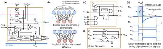
Figure 3.
(a) Schematic of the integrate-and-fire Neuron for neural learning; (b) competitive learning uses explicit one-on-one inhibitory connections, whereas the same function can be implemented with implicit inhibition on a shared winner take-all (WTA) bus; (c) the asynchronous WTA bus interface circuit [44]; (d) spike generator circuit for spikes shown in (e) with rectangular positive tail during the training as well as inference mode, and an exponentially decaying negative tail during the training mode (i.e., when signal T = 1).
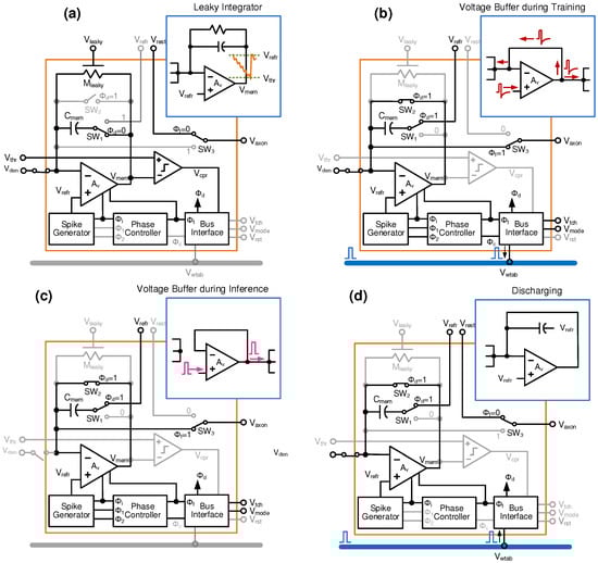
Figure 4.
Event-driven operation of the proposed leaky integrate-and-fire neuron during training and inference.
During the training phase, i.e., when the signal T = 1, the voltage spikes with positive pulse and negative tail are propagated in the forward (pre spikes) as well as the backward direction (post spikes). This enables learning by adjusting the synaptic weights () using STDP based program or erase mechanism seen in Figure 2. During inference (i.e., when T = 0), only the pre-spikes are propagated in the forward direction, and those too with the positive header. Here, no learning takes place and the synaptic weights are preserved while ‘reading’ them. This modification to the neuron circuit, where the negative tail is turned off during inference, is presented for the first time in this article.
After the spike event concludes, the neuron returns to the background integration mode after a refractory period . A fourth mode, called discharge mode, allows competition between neurons. All the neurons are connected using a shared WTA bus; if a winner neuron fires first, other neurons are discharged to discourage them from spiking, forming a powerful neural learning motif [44]. A chip was designed using an earlier version of this neuron where associative learning (Pavlov’s dog experiment) was demonstrated [59]. In this chip fabricated in 180-nm CMOS, neurons generated voltage spikes with configurable parameters to be interfaced with a wide variety of RRAMs. A possible interfacing with CBRAM is shown in Figure 5. The CBRAM device chip was obtained from Prof. Mitkova’s group [70,71,72].
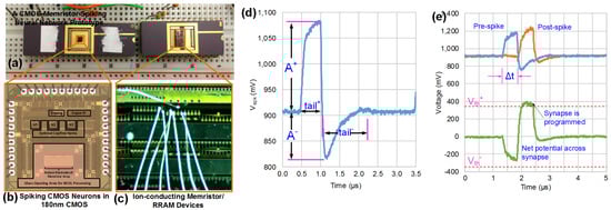
Figure 5.
RRAM-compatible CMOS Neuron: (a) a CMOS-RRAM experimental prototype with (b) 180-nm CMOS spiking neuron chips with digital reconfigurability, and (c) possible interfacing with conductive bridge random access memory (CBRAM) devices [70,71,72]; (d) measured spike output for one of the settings; (e) pre- and post-spike voltage difference applied across a synapse [59].
3.4. Spike-Based Neural Learning Algorithms
SNNs are gaining momentum due to their biological plausibility as well as the potential for low-power hardware implementation. Recently, it was analytically shown that WTA with exponential STDP realizes a powerful unsupervised learning motif that implements expectation maximization; network weights converge to the log probability of the hidden input cause [8,73]. The authors developed algorithms that were compatible with the presented circuits to demonstrate general-purpose pattern recognition engine that consumes ultra-low energy, and were applied to handwritten digit recognition tasks [44,60]. A WTA shared bus architecture with novel event-driven switched-capacitor CMOS neurons was demonstrated. The architecture allows unsupervised as well as supervised competitive learning with significant reduction in hardware complexity and chip area [44]. This two-layer network was simulated with transistor-level circuits using Cadence Spectre for classification of the University of California Irvine (UCI) handwritten digits dataset. Here, a teacher signal was used that only allows the desired neuron to fire based on WTA structure and STDP mechanism for a given output label in the training set.
This semi-supervised spiking network achieved a classification accuracy of 94% for four digits and 83% on all ten digits with around 1000 training samples for each image label. Here, Figure 6 shows the evolution of synaptic weights for each of the ten output neurons as the learning progresses during the training period. Here, we can see that each neuron specializes in detecting only one of the digits and multilevel weights allow higher classification accuracy by emphasizing on critical features of the digits. In the same experiments with binary synapse models, the classification accuracy drops below 80% [44].
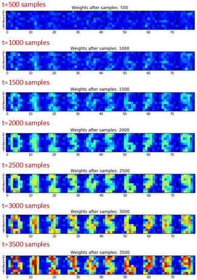
Figure 6.
Evolution of simulated synaptic weights (normalized to the color scale) in the SNN for handwritten character classification.
Deep Learning Using SNNs: Higher classification accuracy can be potentially achieved by increasing the number of competing neurons [74] and/or stacking these spiking WTA motifs with backpropagation (or backprop) algorithm adapted to the SNNs, a challenging task due to the non-differentiable nature of spiking neurons. Recently, there was a successful demonstration of transfer learning whereby first a standard deep ANN was trained and its weights were then transferred to an equivalent SNN achieving close to 99% accuracy on the MNIST handwritten digits dataset [75]. In comparison, the state-of-the-art classification accuracies for the same dataset using conventional deep learning are 99.6% [76] and 99.79% (DropConnect) [77]. Demonstration of transfer learning in SNNs was followed by attempts at spike-based backprop that used membrane potential as a differentiable function [78] or developed differential stochastic neuron models [79]. In parallel, unsupervised deep spike-based convolutional neural networks (ConvNets) based on sparse-coded spikes with WTA and STDP have claimed >98% classification accuracy for the MNIST handwritten digit dataset [80,81].
Backprop for Deep SNNs: There is a growing interest in developing backprop for deep SNNs with some success [79,82]. The reader is referred to the lucid treatment of conventional deep learning using backprop provided in [83] for context and mathematical background. Backprop essentially assigns credits across the neural network layers, which minimizes the overall classification error at the output layer. Standard backprop algorithm relies on the availability of network-wide weights and activation function output and slope information that is stored in high-precision memory. This high-precision memory is accessed using von Neumann bottlenecks, which is precisely the problem we are trying to solve using neuromorphic computing [79]. Implementation of standard backprop on neuromorphic substrates is challenging due to: (1) the weight transport problem as the transpose of the weight matrix, , must be available for computing weight updates at each layer, (2) precise computations of the derivatives of activations functions and multiplications are needed, and (3) the SNN must alternate between forward and backward propagation phases during training [79]. Since the input–output characteristics of a spiking neuron is not differentiable, computing the derivative of its activation function is not directly feasible.
The weight transport bottleneck was mitigated by the development of Random Backprop (RBP) algorithm by Lillicrap [84], where fixed random weight matrix (B) and the output layer error are used for computing all the weight updates in the intermediate layers. Switching to the fixed matrix B from significantly simplifies computation with performance comparable to standard backprop and the backward pass is avoided.
Next, Neftci [79] adapted RBP by recasting it for event-driven SNNs and developed a simplified differentiable model for stochastic spiking neurons. By modeling the membrane potential of the integrate-and-fire neuron with noisy inputs (a valid assumption with circuit noise and/or noisy spike inputs) as a type of Brownian motion, a closed-form expression to relate the input and output firing rates of the neuron was determined, and thus its derivative. Combining RBP with differential stochastic neuron model led to the event-driven random backprop (eRBP) algorithm in [79] resulting in an accuracy of 97.4% for the MNIST handwritten characters dataset. However, the eRBP algorithm abandoned WTA with STDP motifs for local competitive learning, digressing from the understanding derived from computational neuroscience [8,85]. In another parallel work, the WTA motif was included in order to derive backprop equations for SNNs, but STDP was not included [78]. The best case classification accuracy reported in this work for the MNIST handwritten digits dataset was 98.71%.
Even though spike-based backprop, in its current form, may not be the actual algorithm responsible for computation occurring in a biological brain. Nevertheless, it provides an intermittent solution to cognitive applications desired by the computing community. Needless to say, development of learning algorithms for SNN is a promising area of research and, together with developments in the field of computational neuroscience, it may lead to better understanding of brain computation. However, going forward with the development of large-scale NeuSoC architectures, these algorithms must be re-casted based upon the behavior of the synaptic devices such as in the work from IBM [31], where STDP was modified to accommodate abrupt reset or erase operation in (LTD) in PCM-based synapses.
3.5. Challenges with Emerging Devices as Synapses
Contemporary memristive or RRAM devices exhibit several limitations when considered for realizing neuromorphic computing:
(1) Resistive Loading: Resistive loads are typically avoided in CMOS circuits due to the resulting static power consumption. Consequently, large load resistance range is desirable to minimize power consumption in the CMOS neuron circuits that would drive a large number of such resistive devices in parallel. As analyzed later in Section 5, a value of >10 M for the low-resistance state (LRS) or ‘On’ state is needed for obtaining orders of magnitude improvement in energy-efficiency over GPUs. On the other extreme, a very large LRS resistance, say 1 G, will result in extremely low signal-to-noise ratio (SNR) in presence of circuit noise. Thus, the design of resistive memory device structure and the material stack needs to take these trade-offs into consideration.
(2) Variability and Stochasticity: RRAM devices exhibit significant variations (across different devices) and stochasticity (in the same device) in their behavior. This is observed as the program/erase threshold voltages () exhibit stochasticity and variability that in turn depends upon: (1) the initial ‘electroforming’ or ‘breaking-in’ step where the filament is formed in a pristine RRAM cell [86]. The program threshold voltage required for creating a filament (or phase change in the bulk) depends upon the compliance current () and consequently the range of resistance for the LRS state. For example, a low compliance of = 50 nA creates a narrow and weak filament which displays analog-like incremental resistance change behavior, concomitant with large variation in the LRS resistance. Furthermore, these analog-like states may relax to another value within seconds to hours. On the other hand, a large compliance current, say = 5 A, results in a thick filament that exhibits bistable switching behavior with lower variance in the LRS range. Moreover, independently setting the compliance current in a crossbar array in a NeuSoC is unwieldy due to large circuit overhead incurred.
(3) Resolution and Retention: Experimental studies have shown that it can be challenging to obtain stable weights for more than a single-bit resolution in RRAMs, especially without applying compliance current. In some studies, multi-level resistance in oxide-based memristive devices has been observed by fine-tuning the device fabrication and/or electrical pulses for program and erase [86,87]. Analog state retention in actual crossbar circuit configuration of these multi-level RRAMs is presently being studied [87]. Multi-level states have been demonstrated when programming PCM devices; however, the erase operation is abrupt [9,31]. Fundamentally, realizing multiple stable resistance states can be challenging due to the fact that a sufficiently large energy barrier is needed to separate two adjacent resistance states, which is not overcome by thermal energy, leakage or disturbance during the read (inference) operation.
Furthermore, we recently showed, using a simple CMOS emulator circuit, that the pinched hysteresis characteristics of a conceptual memristor doesn’t guarantee analog state retention [24,48]. Based on this discussion, we can assume the worst case scenario that many such RRAM devices in crossbar arrays, with or without setting compliance current, may end up as bistable nonvolatile memory cells.
(4) Polarity: RRAM devices can exhibit either bipolar or unipolar switching characteristics depending upon their material composition. Most RRAMs are employed with bipolar switching where program (Set) and erase (Reset) operations require positive and negative voltage polarity to be applied across the device. On the other hand, unipolar switching devices only use single voltage polarity for program and erase operations [37]. Several filament-based RRAM and CBRAM devices exhibit asymmetric bipolar switching (i.e., the erase threshold is much smaller in magnitude than the program threshold ). This is due to the fact that only a small amount of negative voltage can break or dissolve the filament and erase the device to its high resistance state (HRS) [37,70]. Unipolar and asymmetric bipolar switching characteristics may not be compatible with the STDP scheme shown earlier in Figure 3 and requires circuit modification at the neuron–synapse interface.
(5) Endurance: Since training algorithms continually update network weights while being trained on massive amount of data, synaptic device endurance ultimately governs the in situ on-chip learning capability in a NeuSoC chip. For example, floating-gate or Flash devices are better suited for inference tasks [33] due to < cycles of write endurance [32] , while suitably engineered phase-change memory devices can last for > write cycles [35]. On the other hand, RRAM devices are expected to endure more than write cycles, which makes them promising for continuous online learning on a chip [37].
4. Bio-Inspiration for Higher-Resolution Synapses
Presynaptic and postsynaptic neural activity enables the chemical synapses to change their weights or strengths of connection via biological mechanisms such as LTD and LTP in an adult human brain. This activity dependent synaptic plasticity is evidently the basis of learning and memory in the human brain [3,88]. As evidence of the role played by activity dependent synaptic plasticity in learning and memory is gathered, our understanding of the underlying ‘algorithm’ for cognition in the brain also evolves.
As shown in Figure 7, a biological neuron cell has a body called ‘soma’ with a long axonal tail. The axon branches into axonal terminals or ‘telodendria.’ The soma has projections called dendrites. Synapses are created at the junction between axon terminal of presynaptic neuron and the dendrite on the postsynaptic neuron (soma). Each axonal terminal comprises of thousands of synaptic vesicles, which in turn each contain thousands of neurotransmitter molecules [3]. Neurotransmitters are biochemical molecules that play a vital role in signal transduction between the neurons. In response to an electrical stimulation and resulting Ca influx in the pre-synaptic axon terminal, neurotransmitters are released from synaptic vesicles where they are stored into the synaptic cleft. These biochemical molecules then bind to their specific receptors in the dendrites of the post-synaptic neuron that eventually lead to the opening of ligand-gated ion channels and thus generating an action potential. The whole process takes under two milliseconds of time [3]. The timing between presynaptic and postsynaptic action potential determines the synaptic plasticity and is mediated through biological events such as long-term potentiation and depression of synaptic transmission. The action potential that travels across the axon of postsynaptic neuron is also responsible for initiating a voltage spike in dendrites from which it originated, known as backpropagating action potential (spike). This is now known to be a critical step in synaptic plasticity and involves calcium influx into the dendritic spine.
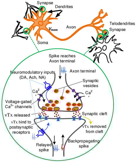
Figure 7.
Synapses are present at the junction of axonal terminal and dendrites of the biological neurons. Some of the known neurotransmitter (Tx) signaling mechanisms are illustrated.
The timing of the spike, amount of calcium influx and distance of dendrites from neuron body determines the degree of the LTP. Dendrites also play a role in neural signal processing through signal attenuation and potentially modification of STDP. The LTD mechanism is still not yet well established. The signal transduction pathways activated by calcium transients in dendrites can impact plasticity by gene activation and synthesis of new proteins that can further modify neurotransmitter release from presynaptic membrane and the number of receptors at the post synaptic membrane. These biological processes are known to affect synaptic plasticity and has been a source of continued research and insight for understanding the learning rules at the individual synaptic level. An axon terminal can contain more than one type of neurotransmitter. The small molecule neurotransmitters such as glutamate, glycine mediate the fast responses of synaptic transmission, whereas the neuropeptide transmitters, as well as the biogenic amines like (DA) and acetylcholine (Ach) and some other small-molecule neurotransmitters, are involved in regulation of neuronal activity and thus the learning rate [3]. Thus, the principle neuromodulatory effect is to gate plasticity by modifying the STDP learning window [89].
Further understanding of neuromodulation mechanisms will help us determine the actual learning mechanism in the brain at the abstraction level of large networks. We now know that dendrites also have a role through nonlinear spike processing and potential modification of STDP [90]. Conclusions from experimental studies are divided over the assertion whether synaptic plasticity is discrete [91] or analog [92] in short-term and long-term dynamics [88]. The difficulty in experimental verification of the discrete plasticity hypothesis arises from the fact that the neurotransmitter release is a stochastic phenomenon and the associated noise can render the discretized step to look continuously varying. In addition, it is known that: (1) synapses are located at varying distances on the soma, (2) spikes undergo a varying amount of nonlinear post-synaptic dendritic filtering, and (3) multiple synaptic connections exist between two neurons in the brain. Consequently, the overall synaptic weight would appear to be analog due to averaging in experiments. For further details, the reader is referred to [88] and the references therein. Further discussion in this article relies upon the bio-plausible hypothesis of discrete, stochastic synapses with dendritic attenuation to realize compound synapses using bistable RRAM devices in parallel.
There is a continual flow of ideas from the computational neuroscience community where they mathematically model and analyze the underlying principles behind neural computing and the role of plasticity, neuromodulation and inhibition. Novel insights lead to refinement of learning algorithms with an ultimate goal of replacing backpropagation by a more biology-like unsupervised and lifelong learning. Implementation of these ideas in circuits follows naturally. At this point, the role of supporting neural cells such as glia and astrocytes, which is comprised of almost half the neural mass, are not well understood; they are ignored in neuromorphic computing until their role becomes clear and significant.
4.1. Compound Synapse with Axonal and Dendritic Processing
The limitations of current memristive or RRAM devices pose a challenge to the realization of continuous-valued synaptic weights with reasonable resolution. Recent work has demonstrated binary-weighted SNNs with 1% to 3% drop in classification accuracy [93]. Other SNN studies have established that synaptic weights with ≥4 bit resolution are required for no significant loss of accuracy [25]. In order to obtain more than binary resolution with the worst-case scenario of bistable RRAM devices, compound synapses were introduced in [94]. Here, several (say ) stochastic memristors were employed in parallel to obtain an approximate resolution of bits on average. This concept was extended to include presynapstic axonal attenuation with parallel stochastic switching RRAMs [95,96]. Recently, the concept was further expanded to combine axonal (presynaptic) as well as dendritic (postsynaptic) processing [55]. This is shown in Figure 8 where parallel RRAM devices are organized in a 2D sub-array structure with spike attenuation being introduced in pre as well as postsynaptic paths. The postsynaptic path is analogous to dendritic processing in biology, while axonal processing is an artificial modification. Fundamentally, in this configuration for the same pre- and post-spike delay (), each stochastic RRAM device is subjected to a different pulse voltage across it and thus has distinct probability of switching. A smaller causes more individual RRAMs to switch than a larger value of , thus providing flexibility in controlling the STDP behavior.
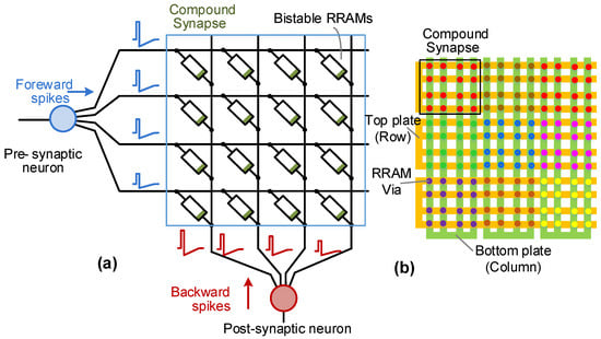
Figure 8.
(a) A compound synapse in a dendritic configuration with M = 16 parallel bistable RRAMs; (b) a possible layout configuration for the compound synapse.
The compound synapse concept with dendritic processing is biologically plausible as the STDP updates can be hypothesized to be discrete and stochastic, similar to the probabilistic release of the neurotransmitters. When averaged over a large number of synapses with individual dendritic attenuation, the discrete probabilistic plasticity emulates continuous analog-like behavior. Figure 9 shows the simulation results for the proposed concept. In this simulation, RRAMs are employed with pre and post synaptic attenuations. Assuming Gaussian distribution of the program/erase threshold voltages, the stochastic switching behavior of the bistable RRAM device is given by cumulative probability for a voltage drop of V across the device. This is expressed as [95,96]
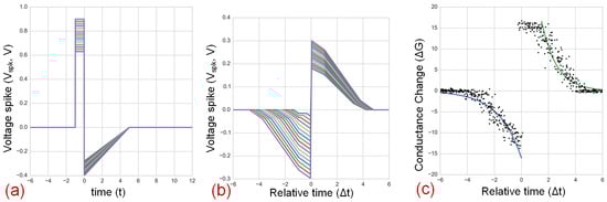
Figure 9.
(a) Simulated spike waveforms with dendritic attenuations; (b) effective potential difference across parallel devices versus ; 16 levels are created over program and erase thresholds and ; (c) simulated STDP learning window with dendritic processing.
is the mean threshold voltages with as the standard deviation. In this simulation, we have chosen program and erase threshold mean values as V and V, respectively, with the same V. Here, is the tail distribution of the standard normal distribution. The LRS conductance of a bistable RRAM is of one unit and HRS conductance is assumed to be zero.
In the compound synapse, the conductance of individual bistable RRAMs will add up to form multi-level weight given by , where is the conductance of the individual bistable RRAM device between pre-neuron i and post-neuron j, and M is the total number of RRAMs in the synapse. The post-synaptic neuron integrates the current given by , where are the spikes from pre-neurons. If RRAM devices are always stuck in their LRS state due to low threshold voltage corner (based on process or electroforming variations), those particular devices may not switch, but other devices will continue to provide stochastic switching. Thus, it is important to ensure that the RRAMs are always operated in the stochastic regime based on extensive statistical device characterization and tunable voltage spike parameters on chip.
In this setup, both axonal attenuations and dendritic attenuations are set to a pre-selected range of varying attenuations from 0.8 to 1. These produce 16 positive and 16 negative voltage levels shown in Figure 9a. Due to this staggering of pulse voltages, each RRAM experiences distinct switching probability as a function of as in Figure 9b. Figure 9c shows the STDP learning window with normalized change in the conductance (Dw) of the compound synapse with dendrites.
The plots in Figure 9c demonstrate 16 levels of , both in the LTP (positive) and LTD (negative) side of the STDP window. These 16 levels result in 4-bit resolution on average. Each dot in the plots represents the probability density of the particular transition between −16 and 16. With dendritic processing, a double exponential curve is fitted to the simulated STDP window with <1-unit fitting error; STDP window without dendrites has approximately 4-unit error when fitted to the double exponential [95,96]. Moreover, the axonal and dendrite coefficients, and , and potentially their respective time delays, can be customized to implement a wide range of STDP learning windows. In future work, in addition to including nonlinear processing, tuning of coefficients during training can allow inclusion of neuromodulation effects, where global error feedback signals can modulate local synaptic plasticity. In summary, combining dendritic processing schemes with stochastic RRAMs can allow a high degree of freedom in implementing high-resolution STDP weights.
4.2. Modified CMOS Neuron with Dendritic Processing
An event-driven integrate-and-fire neuron circuit is adapted from the discussion in Section 3 and shown in Figure 10. Here, dendritic processing is realized by allowing parallel outputs with different gains/attenuations. The dendrites can be implemented using self-biased source follower (SF) based buffers with varying attenuations. The output impedance of the source follower buffers is designed to be smaller than the equivalent LRS resistance of the devices in parallel (). Since the buffers external to the opamp in the CMOS neuron drive the resistive synapses, the power consumption of the opamp is considerably reduced. Consequently, single-stage opamp with ≈40 dB gain and large input swing is sufficient to realize the neuron. Furthermore, splitting the buffers needed to drive the RRAM synapses for each dendrite allows larger synaptic fan-outs. The pre-synaptic buffers in the axonal path, needed for backpropagating the spikes, require some thought. During the integration phase, these buffers should allow the input current to be summed at the opamp’s virtual ground and integrated in the membrane capacitance. Thus, the axonal buffers are bypassed when the neuron is in the integration phase as shown in Figure 10. In the future, nonlinearity in the dendritic circuits can be explored for realizing higher resolution with bistable RRAM synapses, as observed in neurobiology experiments.
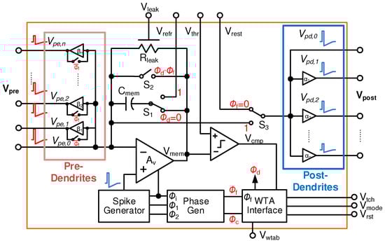
Figure 10.
A simplified schematic of a spiking CMOS neuron modified to accommodate pre-synaptic axonal and post-synaptic dendritic attenuations.
5. Energy-Efficiency of Neuromorphic SoCs
The fundamental reason for investigating NVM or RRAM based NeuSoC architectures is to realize several orders of magnitude improvement in energy-efficiency over the digital ASICs and GPUs, and significantly higher neurosynaptic density when compared to contemporary neuromorphic chips that use digital SRAM synapses. As discussed earlier, resistive loading of CMOS neuron circuits by the resistive synapses poses severe limitations on the achievable energy-efficiency of the NeuSoCs. In the discussed NeuSoC architecture, two factors primarily determine the energy-efficiency at the circuit level, namely the spike shape parameters (i.e., voltage and pulse width) and the range of the LRS, . The HRS range is typically order(s) of magnitude higher than and thus can be ignored in the energy-efficiency calculations. The off/on ratio is an important parameter that denotes the range over which the device can be programmed and impacts the resulting SNR during inference operation. The spike pulse shapes were shown in Figure 3. The spike pulse shape has an amplitude and pulse-width of during the inference mode. Thus, the current input signal is and the energy consumed in driving a synapse is given by [24]
where is the resistance of the synapse with a range . In this calculation, compound synapses with dendritic processing and RRAM devices in parallel are employed to achieve an equivalent analog synapse with 4-bit resolution. Learning algorithm considerations such as the input encoding, neuron sparsity (i.e., the percentage of synapses in LRS state), neuron spike-rate adaptation and homeostasis also determine the energy-efficiency of the overall NeuSoC. For a single instance of training or inference on an input pattern, the energy, , consumed in the spiking neural network is approximated as [96]
where is the total number of neurons, is the total number of synaptic connections in the SNN, is the fraction of synapses in the LRS state, is the neuron static power consumption and the neuron sparsity factor is . Furthermore, energy dissipated in the peripheral circuits and interconnects outside the neurosynpatic array is ignored for the benefit of analytical simplicity.
For benchmarking the NeuSoC architecture performance, we employ AlexNet deep Convolutional Neural Network (CNN) that was the winner of the Imagenet Computer Vision Challenge [97] in 2012. Alexnet neural network was trained on then state-of-the-art Nvidia P4 GPU (Santa Clara, CA, USA), had 640 k neurons with 61 million synapses and a classification energy-efficiency of 170 images/second/Watt [98]. In this analysis, we envisage an equivalent SNN that can achieve classification accuracy within error as that of the deep neural network trained on a GPU. We assume that this can be achieved by leveraging transfer learning [75] in an SNN, and/or by employing spike-based equivalent of the backpropagation or similar algorithms [79]. Thus, the overall circuit architecture is essentially the same as that of the standard ANN but implemented using mixed-signal neurons and RRAM synapse arrays.
The numerical estimates are based on: (1) our RRAM-compatible spiking neuron chip described in [59], (2) 4-bit compound memristive synapses [55,94,95], and (3) ranging from 0.1–10 M. The energy consumption for processing (training or classification) of one image is shown in Table 1. By comparing with the contemporary GPU Nvidia P4 [98] (170 images/s/W), a memristive architecture with = 100 k provides a meager improvement in energy-efficiency. However, the energy consumption can be significantly reduced if the LRS resistance of the memristive devices can be increased to high-M regime, leading to a potential range performance improvement; high LRS also helps reduce the power consumption in the opamp-based neuron circuits [24,59,96,99]. This analysis suggests that the energy-efficiency can be improved solely by increasing the LRS resistance of the RRAM devices. However, there has been less focus on realizing high-LRS-resistance devices as the multi-valued memristive devices are still under development. High-LRS-resistance could potentially be achieved by controlling the compliance current, optimizing material stoichiometry in transition oxide RRAMs [86,87], or by engineering entirely new type of devices.

Table 1.
Energy estimation for a NeuSoC employing compound resistive random access memory (RRAM) compound synapse with M = 16 parallel devices.
6. Towards Large-Scale Neuromorphic SoCs
We have described the underlying device design and operation trade-offs for the emerging memory devices in NeuSoC applications. The write (Program/Erase) and read pulse voltages and temporal profile govern the fundamental trade-offs between performance parameters such as the state retention, stochasticity, crossbar array size and impact of sneak-paths, device endurance, and energy consumption. The LRS resistance governs the energy-efficiency of the NeuSoC. However, the synapse resistance range trades off with the available SNR during inference; a higher HRS resistance would result in the current being integrated to be of the same order as the thermal and flicker noise in the CMOS neuron. The synapse resistance range (or the ratio), synapse stochasticity, and the inference SNR ultimately determine the learning and classification performance of the deep learning architectures. For example, we may require higher endurance if the NeuSoC continually trains while in operation or weight updates exceeding the write cycle endurance are desired during the chip life time. This may require applying lower stress to the devices that can result in higher stochasticity. The amount of stochasticity directly impacts the state retention (more state leakage or relaxation for higher stochasticity). Thus, it is imperative that the device optimization cannot be decoupled from the circuit and system-level requirements driven by the application.
Furthermore, stochastity provides a viable approach for multi-bit synpase realization using realistic devices. In the near-term, the crossbar circuit architecture will continually advance to realize ConvNets and implement the emerging learning algorithms where error feedback (such as in backprop) can be implemented using evolving mechanisms such as neuromodulated STDP [89], random backprop [79,84], or through explicit computation of gradients.
Another major challenge for neuromorphic computing is continuous on-device learning with smaller amount of data, as opposed to Big Data, similar to biological brains. Contemporary deep learning requires a large amount of data for training neural networks using stochastic gradient descent with mini-batches [83]. Gradient descent or backprop-based approaches inherently suffer from catastrophic forgetting in sequential learning as later weight updates cause the network to forget the previously learned representations [100]. Recent solutions to catastrophic learning employ elastic weight consolidation (EWC) [100] or neuron selection for selective weight updates [101]. On the other hand, STDP-based unsupervised deep learning approaches [7,80] that do not use backprop are promising and an active area of investigation. However, further research is needed to consistently achieve performance comparable to deep learning.
Finally, large scale NeuSoCs require development across the entire system hierarchy—(1) densely integrated nonvolatile devices with long-term retention and endurance and higher LRS resistance, (2) ultra-low-power event-driven mixed-signal circuits that can interface with crossbar devices and scale to multiple layers of deep spiking neural networks as seen in Figure 1, and (3) learning algorithms that can train the on-chip neural networks with localized learning within the write endurance limit of the underlying devices. Energy-efficiency analysis of the NeuSoC architecture for realizing large-scale neural networks in Section 5 provides guidance for the target specifications for devices and circuits, and the sparsity for the spiking activity (algorithms) so that the devices don’t wear out quickly. The on-chip data flow can be managed by juxtaposition of crossbar arrays. However, as the neural networks scale to large chips or across several chips, high-bandwidth interconnects become indispensable. Asynchronous Address-event representation (AER) interconnects were developed to interface neuromorphic devices and chips [15,102] before the advent of deep learning. However, AER-based interconnects need to be revisited and adapted to the high-throughput, lower latency and connectivity demanded by deep spiking neural networks. Recent advances in interconnects include asynchronous network-on-chip communication used in TrueNorth [12], Loihi [14] and SpiNNaker [13], and time-domain multiplexing [103].
7. Conclusions
This article provides a review of the application of RRAM synapses to mixed-signal neuromorphic computing and challenges involved in their interfacing with CMOS neuron circuits. The interplay of devices, circuits and algorithm is important and their co-development is critical in optimizing the overall energy-efficiency of large-scale NeuSoC architectures and bringing it closer to the brain-like efficiency. With continued progress, such neuromorphic architectures pave the path for computing beyond the limitations set by the Moore’s scaling of CMOS transistors and the energy bottleneck of von Neumann computers. Moreover, such NeuSoCs open the possibility of realizing general purpose Artificial Intelligence in portable devices instead of always relying upon the energy-intensive Cloud infrastructure. In doing so, NeuSoCs provide a newer avenue for novel memory technology development, where memory itself can be the next generation platform, integral to computing.
Author Contributions
X.W. and V.S. conceived and designed the experiments; X.W. designed the chip and performed the experiments; X.W. and V.S. analyzed the data; I.S. contributed analysis on bio-plausibility of methods; K.Z. helped with the chip design and tests. V.S. coordinated the writing of the paper.
Funding
The authors gratefully acknowledge partial support through U.S. National Science Foundation (NSF) awards CCF-1320987 and EECS-1454411, and Micron Foundation for the Micron Endowed Professorship for Vishal Saxena.
Acknowledgments
The authors also thank John Chiasson and Ruthvik Vaila for technical discussions on spiking neural networks and learning algorithms. We are also extremely grateful to Maria Mitkova and her research group for samples, discussions and experimental insights on CBRAM devices.
Conflicts of Interest
The authors declare no conflict of interest.
Abbreviations
The following abbreviations are used in this manuscript:
| AI | Artificial Intelligence |
| ANN | Artificial Neural Network |
| ASIC | Application Specific Integrated Circuit |
| CBRAM | Conductive Bridge Random Access Memory |
| CMOS | Complementary Metal Oxide Semiconductor |
| CNN | Convolutional Neural Network |
| DAC | Digital-to-Analog Converter |
| eRBP | Event-Driven Random Backpropagation |
| FPGA | Field Programmable Gate Array |
| GPU | Graphics Processing Unit |
| HRS | High-Resistance State |
| IC | Integrated Circuit |
| ICA | Intelligent Cognitive Assistants |
| LRS | Low-Resistance State |
| LTD | Long-Term Depression |
| LTP | Long-Term Potentiation |
| NVM | Non-Volatile Memory |
| PCM | Phase Change Memory |
| PCRAM | Phase Change Random Access Memory |
| RRAM | Resistive Random Access Memory |
| SF | Source Follower |
| RBP | Random Backpropagation |
| SRAM | Static Random Access Memory |
| SNN | Spiking Neural Networks |
| SNR | Signal-to-Noise Ratio |
| STDP | Spike-Timing Dependent Plasticity |
| STTRAM | Spin-Transfer Torque Random Access Memory |
| TSV | Through-Silicon Via |
| NeuSoC | Neuromorphic System-on-a-Chip |
| VLSI | Very Large Scale Integrated Circuits |
| WTA | Winner Take All |
References
- Williams, R.; DeBenedictis, E.P. OSTP Nanotechnology-Inspired Grand Challenge: Sensible Machines. In IEEE Rebooting Computing Whitepaper; 2015; Available online: http://www.webcitation.org/72ppzDEKx (accessed on 30 September 2018).
- Hinton, G.E.; Salakhutdinov, R.R. Reducing the dimensionality of data with neural networks. Science 2006, 313, 504–507. [Google Scholar] [CrossRef] [PubMed]
- Kandel, E.R.; Schwartz, J.H.; Jessell, T.M.; Siegelbaum, S.A.; Hudspeth, A.J. Principles of Neural Science; McGraw-Hill: New York, NY, USA, 2000; Volume 4. [Google Scholar]
- Krzanich, B. Intel Pioneers New Technologies to Advance Artificial Intelligence. Available online: http://www.webcitation.org/72pqcyFZF (accessed on 30 September 2018).
- Bi, G.Q.; Poo, M.M. Synaptic modification by correlated activity: Hebb’s postulate revisited. Annu. Rev. Neurosci. 2001, 24, 139–166. [Google Scholar] [CrossRef] [PubMed]
- Dan, Y.; Poo, M.M. Spike timing-dependent plasticity of neural circuits. Neuron 2004, 44, 23–30. [Google Scholar] [CrossRef] [PubMed]
- Masquelier, T.; Thorpe, S.J. Unsupervised Learning of Visual Features through Spike Timing Dependent Plasticity. PLoS Comput. Biol. 2007, 3, e31. [Google Scholar] [CrossRef] [PubMed]
- Nessler, B.; Pfeiffer, M.; Buesing, L.; Maass, W. Bayesian computation emerges in generic cortical microcircuits through spike-timing-dependent plasticity. PLoS Comput. Biol. 2013, 9, e1003037. [Google Scholar] [CrossRef] [PubMed]
- Burr, G.W.; Shelby, R.M.; Sebastian, A.; Kim, S.; Kim, S.; Sidler, S.; Virwani, K.; Ishii, M.; Narayanan, P.; Fumarola, A.; et al. Neuromorphic computing using non-volatile memory. Adv. Phys. 2017, 2, 89–124. [Google Scholar] [CrossRef]
- James, C.D.; Aimone, J.B.; Miner, N.E.; Vineyard, C.M.; Rothganger, F.H.; Carlson, K.D.; Mulder, S.A.; Draelos, T.J.; Faust, A.; Marinella, M.J.; et al. A historical survey of algorithms and hardware architectures for neural-inspired and neuromorphic computing applications. Biol. Inspired Cogn. Architect. 2017, 19, 49–64. [Google Scholar] [CrossRef]
- Schuman, C.D.; Potok, T.E.; Patton, R.M.; Birdwell, J.D.; Dean, M.E.; Rose, G.S.; Plank, J.S. A survey of neuromorphic computing and neural networks in hardware. arXiv, 2017; arXiv:1705.06963. [Google Scholar]
- Merolla, P.A.; Arthur, J.V.; Alverez-Icaza, R.; Cassidy, A.S.; Sawada, J.; Akopyan, F.; Jackson, B.L.; Imam, N.; Guo, C.; Nakamura, Y.; et al. A million spiking-neuron integrated circuit with a scalable communication network and interface. Sci. Mag. 2014, 345, 668–673. [Google Scholar] [CrossRef] [PubMed]
- Painkras, E.; Plana, L.; Garside, J.; Temple, S.; Davidson, S.; Pepper, J.; Clark, D.; Patterson, C.; Furber, S. Spinnaker: A multi-core system-on-chip for massively-parallel neural net simulation. In Proceedings of the 2012 IEEE Custom Integrated Circuits Conference (CICC), San Jose, CA, USA, 9–12 September 2012; pp. 1–4. [Google Scholar]
- Davies, M.; Srinivasa, N.; Lin, T.H.; Chinya, G.; Cao, Y.; Choday, S.H.; Dimou, G.; Joshi, P.; Imam, N.; Jain, S.; et al. Loihi: A neuromorphic manycore processor with on-chip learning. IEEE Micro 2018, 38, 82–99. [Google Scholar] [CrossRef]
- Liu, S.C. Event-Based Neuromorphic Systems; John Wiley & Sons: Hoboken, NJ, USA, 2015. [Google Scholar]
- Indiveri, G. Neuromorphic Bisable VLSI Synapses with Spike-Timing-Dependent Plasticity. In Proceedings of the Neural Information Processing Systems 2003, Vancouver, BC, Canada, 8–13 December 2003; pp. 1115–1122. [Google Scholar]
- Fusi, S.; Annunziato, M.; Badoni, D.; Salamon, A.; Amit, D.J. Spike-driven synaptic plasticity: Theory, simulation, VLSI implementation. Neural Comput. 2000, 12, 2227–2258. [Google Scholar] [CrossRef] [PubMed]
- Indiveri, G.; Chicca, E.; Douglas, R. A VLSI reconfigurable network of integrate-and-fire neurons with spike-based learning synapses. In Proceedings of the 2004 European Symposium on Artificial Neural Networks, Bruges Belgium, 28–30 April 2004. [Google Scholar]
- Indiveri, G.; Chicca, E.; Douglas, R. A VLSI array of low-power spiking neurons and bistable synapses with spike-timing dependent plasticity. IEEE Trans. Neural Netw. 2006, 17, 211–221. [Google Scholar] [CrossRef] [PubMed]
- Mitra, S.; Fusi, S.; Indiveri, G. Real-Time Classification of Complex Patterns Using Spike-Based Learning in Neuromorphic VLSI. IEEE Trans. Biomed. Circuits Syst. 2009, 3, 32–42. [Google Scholar] [CrossRef] [PubMed]
- Qiao, N.; Mostafa, H.; Corradi, F.; Osswald, M.; Stefanini, F.; Sumislawska, D.; Indiveri, G. A reconfigurable on-line learning spiking neuromorphic processor comprising 256 neurons and 128 K synapses. Front. Neurosci. 2015, 9, 141. [Google Scholar] [CrossRef] [PubMed]
- Azghadi, M.R.; Iannella, N.; Al-Sarawi, S.F.; Indiveri, G.; Abbott, D. Spike-based synaptic plasticity in silicon: design, implementation, application, and challenges. Proc. IEEE 2014, 102, 717–737. [Google Scholar] [CrossRef]
- Benjamin, B.V.; Gao, P.; McQuinn, E.; Choudhary, S.; Chandrasekaran, A.R.; Bussat, J.M.; Alvarez-Icaza, R.; Arthur, J.V.; Merolla, P.; Boahen, K. Neurogrid: A mixed-analog-digital multichip system for large-scale neural simulations. Proc. IEEE 2014, 102, 699–716. [Google Scholar] [CrossRef]
- Saxena, V.; Wu, X.; Zhu, K. Energy-Efficient CMOS Memristive Synapses for Mixed-Signal Neuromorphic System-on-a-Chip. In Proceedings of the 2018 IEEE International Symposium on Circuits and Systems (ISCAS), Florence, Italy, 27–30 May 2018; pp. 1–5. [Google Scholar]
- Pfeil, T.; Potjans, T.C.; Schrader, S.; Potjans, W.; Schemmel, J.; Diesmann, M.; Meier, K. Is a 4-bit synaptic weight resolution enough?-constraints on enabling spike-timing dependent plasticity in neuromorphic hardware. arXiv, 2012; arXiv:1201.6255. [Google Scholar]
- Neftci, E.; Das, S.; Pedroni, B.; Kreutz-Delgado, K.; Cauwenberghs, G. Event-driven contrastive divergence for spiking neuromorphic systems. Front. Neurosci. 2013, 7, 272. [Google Scholar] [CrossRef] [PubMed]
- Pfeil, T.; Grübl, A.; Jeltsch, S.; Müller, E.; Müller, P.; Petrovici, M.A.; Schmuker, M.; Brüderle, D.; Schemmel, J.; Meier, K. Six networks on a universal neuromorphic computing substrate. Front. Neurosci. 2013, 7, 11. [Google Scholar] [CrossRef] [PubMed]
- Schemmel, J.; Briiderle, D.; Griibl, A.; Hock, M.; Meier, K.; Millner, S. A wafer-scale neuromorphic hardware system for large-scale neural modeling. In Proceedings of the 2010 IEEE International Symposium on Circuits and Systems (ISCAS), Paris, France, 30 May–2 June 2010; pp. 1947–1950. [Google Scholar]
- Brink, S.; Nease, S.; Hasler, P. Computing with networks of spiking neurons on a biophysically motivated floating-gate based neuromorphic integrated circuit. Neural Netw. 2013, 45, 39–49. [Google Scholar] [CrossRef] [PubMed]
- Lu, J.; Young, S.; Arel, I.; Holleman, J. A 1 TOPS/W analog deep machine-learning engine with floating-gate storage in 0.13 μm CMOS. IEEE J. Solid-State Circuits 2015, 50, 270–281. [Google Scholar] [CrossRef]
- Kim, S.; Ishii, M.; Lewis, S.; Perri, T.; BrightSky, M.; Kim, W.; Jordan, R.; Burr, G.; Sosa, N.; Ray, A.; et al. NVM neuromorphic core with 64k-cell (256-by-256) phase change memory synaptic array with on-chip neuron circuits for continuous in situ learning. In Proceedings of the 2015 IEEE International Electron Devices Meeting (IEDM), Washington, DC, USA, 7–9 December 2015. [Google Scholar]
- TN-12-30: NOR Flash Cycling Endurance and Data Retention; Technical Report; Micron Technology Inc.: Boise, ID, USA, 2013.
- Demler, M. Mythic Multiplies in a Flash: Analog In-Memory Computing Eliminates DRAM Read/Write Cycles; Technical Report; Microprocessor Report: Redwood City, CA, USA, 2018. [Google Scholar]
- Burr, G.W.; Shelby, R.M.; Sidler, S.; Di Nolfo, C.; Jang, J.; Boybat, I.; Shenoy, R.S.; Narayanan, P.; Virwani, K.; Giacometti, E.U.; et al. Experimental demonstration and tolerancing of a large-scale neural network (165,000 synapses) using phase-change memory as the synaptic weight element. IEEE Trans. Electron Devices 2015, 62, 3498–3507. [Google Scholar] [CrossRef]
- Burr, G.W.; Brightsky, M.J.; Sebastian, A.; Cheng, H.Y.; Wu, J.Y.; Kim, S.; Sosa, N.E.; Papandreou, N.; Lung, H.L.; Pozidis, H.; et al. Recent progress in phase-change memory technology. IEEE J. Emerg. Sel. Top. Circuits Syst. 2016, 6, 146–162. [Google Scholar] [CrossRef]
- Zhou, Y.; Ramanathan, S. Mott memory and neuromorphic devices. Proc. IEEE 2015, 103, 1289–1310. [Google Scholar] [CrossRef]
- Waser, R.; Ielmini, D.; Akinaga, H.; Shima, H.; Wong, H.S.P.; Yang, J.J.; Yu, S. Introduction to nanoionic elements for information technology. In Resistive Switching: From Fundamentals of Nanoionic Redox Processes to Memristive Device Applications; Wiley: Hoboken, NJ, USA, 2016; pp. 1–30. [Google Scholar]
- Jo, S.H.; Chang, T.; Ebong, I.; Bhadviya, B.B.; Mazumder, P.; Lu, W. Nanoscale memristor device as synapse in neuromorphic systems. Nano Lett. 2010, 10, 1297–1301. [Google Scholar] [CrossRef] [PubMed]
- Li, Y.; Zhong, Y.; Xu, L.; Zhang, J.; Xu, X.; Sun, H.; Miao, X. Ultrafast Synaptic Events in a Chalcogenide Memristor. Sci. Rep. 2013, 3, 1619. [Google Scholar] [CrossRef] [PubMed]
- Yang, J.J.; Strukov, D.B.; Stewart, D.R. Memristive devices for computing. Nat. Nanotechnol. 2013, 8, 13–24. [Google Scholar] [CrossRef] [PubMed]
- Chang, T.; Yang, Y.; Lu, W. Building neuromorphic circuits with memristive devices. IEEE Circuits Syst. Mag. 2013, 13, 56–73. [Google Scholar] [CrossRef]
- Yu, S.; Kuzum, D.; Wong, H.S.P. Design considerations of synaptic device for neuromorphic computing. In Proceedings of the IEEE International Symposium on Circuits and Systems (ISCAS), Melbourne, Australia, 1–5 June 2014; pp. 1062–1065. [Google Scholar]
- Indiveri, G.; Legenstein, R.; Deligeorgis, G.; Prodromakis, T. Integration of Nanoscale Memristor Synapses in Neuromorphic Computing Architectures. Nanotechnology 2013, 24, 384010. [Google Scholar] [CrossRef] [PubMed]
- Wu, X.; Saxena, V.; Zhu, K. Homogeneous Spiking Neuromorphic System for Real-World Pattern Recognition. IEEE J. Emerg. Sel. Top. Circuits Syst. 2015, 5, 254–266. [Google Scholar] [CrossRef]
- Shi, J.; Ha, S.D.; Zhou, Y.; Schoofs, F.; Ramanathan, S. A correlated nickelate synaptic transistor. Nat. Commun. 2013, 4, 2676. [Google Scholar] [CrossRef] [PubMed]
- Fuller, E.J.; Gabaly, F.E.; Léonard, F.; Agarwal, S.; Plimpton, S.J.; Jacobs-Gedrim, R.B.; James, C.D.; Marinella, M.J.; Talin, A.A. Li-ion synaptic transistor for low power analog computing. Adv. Mater. 2016, 29, 1604310. [Google Scholar] [CrossRef] [PubMed]
- Saxena, V. Memory Controlled Circuit System and Apparatus. US Patent Application No. 14/538,600, 1 October 2015. [Google Scholar]
- Saxena, V. A Compact CMOS Memristor Emulator Circuit and its Applications. In Proceedings of the IEEE International Midwest Symposium on Circuits and Systems (MWSCAS), Windsor, ON, Canada, 5–8 August 2018; pp. 1–5. [Google Scholar]
- Govoreanu, B.; Kar, G.; Chen, Y.; Paraschiv, V.; Kubicek, S.; Fantini, A.; Radu, I.; Goux, L.; Clima, S.; Degraeve, R.; et al. 10× 10 nm 2 Hf/HfO x crossbar resistive RAM with excellent performance, reliability and low-energy operation. In Proceedings of the 2011 IEEE International Electron Devices Meeting (IEDM), Washington, DC, USA, 5–7 December 2011; pp. 31–36. [Google Scholar]
- Chen, Y.Y.; Degraeve, R.; Clima, S.; Govoreanu, B.; Goux, L.; Fantini, A.; Kar, G.S.; Pourtois, G.; Groeseneken, G.; Wouters, D.J.; et al. Understanding of the endurance failure in scaled HfO 2-based 1T1R RRAM through vacancy mobility degradation. In Proceedings of the IEEE International Electron Devices Meeting (IEDM), San Francisco, CA, USA, 10–13 December 2012; pp. 20–23. [Google Scholar]
- Kozicki, M.N.; Mitkova, M.; Valov, I. Electrochemical Metallization Memories. In Resistive Switching; Wiley-Blackwell: Hoboken, NJ, USA, 2016; pp. 483–514. [Google Scholar]
- Fong, X.; Kim, Y.; Venkatesan, R.; Choday, S.H.; Raghunathan, A.; Roy, K. Spin-transfer torque memories: Devices, circuits, and systems. Proc. IEEE 2016, 104, 1449–1488. [Google Scholar] [CrossRef]
- Micron. 3D XPointTM Technology: Breakthrough Nonvolatile Memory Technology. Available online: http://www.webcitation.org/72pvm4wn3 (accessed on 30 September 2018).
- Strukov, D.B.; Snider, G.S.; Stewart, D.R.; Williams, R.S. The Missing Memristor Found. Nature 2008, 453, 80. [Google Scholar] [CrossRef] [PubMed]
- Saxena, V.; Wu, X.; Srivastava, I.; Zhu, K. Towards spiking neuromorphic system-on-a-chip with bio-plausible synapses using emerging devices. In Proceedings of the 4th ACM International Conference on Nanoscale Computing and Communication, Washington, DC, USA, 27–29 September 2017; p. 18. [Google Scholar]
- Kuzum, D.; Jeyasingh, R.G.; Lee, B.; Wong, H.S.P. Nanoelectronic programmable synapses based on phase change materials for brain-inspired computing. Nano Lett. 2011, 12, 2179–2186. [Google Scholar] [CrossRef] [PubMed]
- Seo, K.; Kim, I.; Jung, S.; Jo, M.; Park, S.; Park, J.; Shin, J.; Biju, K.P.; Kong, J.; Lee, K.; et al. Analog memory and spike-timing-dependent plasticity characteristics of a nanoscale titanium oxide bilayer resistive switching device. Nanotechnology 2011, 22, 254023. [Google Scholar] [CrossRef] [PubMed]
- Koch, C. Computation and the single neuron. Nature 1997, 385, 207. [Google Scholar] [CrossRef] [PubMed]
- Wu, X.; Saxena, V.; Zhu, K.; Balagopal, S. A CMOS Spiking Neuron for Brain-Inspired Neural Networks With Resistive Synapses and In Situ Learning. IEEE Trans. Circuits Syst. II Express Briefs 2015, 62, 1088–1092. [Google Scholar] [CrossRef]
- Wu, X.; Saxena, V.; Zhu, K. A CMOS Spiking Neuron For Dense Memristor-synapse Connectivity For Brain-inspired Computing. In Proceedings of the International Joint Conference on Neural Networks (IJCNN), Killarney, Ireland, 12–17 July 2015; pp. 1–6. [Google Scholar]
- Serrano-Gotarredona, T.; Prodromakis, T.; Linares-Barranco, B. A proposal for hybrid memristor-CMOS spiking neuromorphic learning systems. IEEE Circuits Syst. Mag. 2013, 13, 74–88. [Google Scholar] [CrossRef]
- Serrano-Gotarredona, T.; Masquelier, T.; Prodromakis, T.; Indiveri, G.; Linares-Barranco, B. STDP and STDP variations with memristors for spiking neuromorphic learning systems. Front. Neurosci. 2013, 7, 2. [Google Scholar] [CrossRef] [PubMed]
- Indiveri, G.; Linares-Barranco, B.; Hamilton, T.J.; Van Schaik, A.; Etienne-Cummings, R.; Delbruck, T.; Liu, S.C.; Dudek, P.; Häfliger, P.; Renaud, S.; et al. Neuromorphic silicon neuron circuits. Front. Neurosci. 2011, 5, 73. [Google Scholar] [CrossRef] [PubMed]
- Joubert, A.; Belhadj, B.; Héliot, R. A robust and compact 65 nm LIF analog neuron for computational purposes. In Proceedings of the 2011 IEEE 9th International New Circuits and Systems Conference (NEWCAS), Bordeaux, France, 26–29 June 2011; pp. 9–12. [Google Scholar]
- Wang, R.; Hamilton, T.J.; Tapson, J.; van Schaik, A. A generalised conductance-based silicon neuron for large-scale spiking neural networks. In Proceedings of the 2014 IEEE International Symposium on Circuits and Systems (ISCAS), Melbourne, Australia, 1–5 June 2014; pp. 1564–1567. [Google Scholar]
- Cruz-Albrecht, J.M.; Yung, M.W.; Srinivasa, N. Energy-efficient neuron, synapse and STDP integrated circuits. IEEE Trans. Biomed. Circuits Syst. 2012, 6, 246–256. [Google Scholar] [CrossRef] [PubMed]
- Sahoo, B.D. Ring oscillator based sub-1V leaky integrate-and-fire neuron circuit. In Proceedings of the 2017 IEEE International Symposium on Circuits and Systems (ISCAS), Baltimore, MD, USA, 28–31 May 2017; pp. 1–4. [Google Scholar]
- Ebong, I.E.; Mazumder, P. CMOS and Memristor-Based Neural Network Design for Position Detection. Proc. IEEE 2012, 100, 2050–2060. [Google Scholar] [CrossRef]
- Serrano-Gotarredona, T.; Linares-Barranco, B. Design of adaptive nano/CMOS neural architectures. In Proceedings of the 2012 19th IEEE International Conference on Electronics, Circuits and Systems (ICECS), Seville, Spain, 9–12 December 2012; pp. 949–952. [Google Scholar]
- Latif, M.R. Nano-Ionic Redox Resistive RAM–Device Performance Enhancement through Materials Engineering, Characterization and Electrical Testing. Ph.D. Thesis, Boise State University, Boise, ID, USA, 2014. [Google Scholar]
- Latif, M.; Csarnovics, I.; Kökényesi, S.; Csik, A.; Mitkova, M. Photolithography-free Ge–Se based memristive arrays; materials characterization and device testing 1. Can. J. Phys. 2013, 92, 623–628. [Google Scholar] [CrossRef]
- Latif, M.R.; Mitkova, M.; Tompa, G.; Coleman, E. PECVD of GexSe1−x films for nano-ionic redox conductive bridge memristive switch memory. In Proceedings of the 2013 IEEE Workshop on Microelectronics and Electron Devices (WMED), Boise, ID, USA, 12 April 2013; pp. 1–4. [Google Scholar]
- Masquelier, T.; Guyonneau, R.; Thorpe, S.J. Spike Timing Dependent Plasticity Finds the Start of Repeating Patterns in Continuous Spike Trains. PLoS ONE 2008, 3, e1377. [Google Scholar] [CrossRef] [PubMed]
- Diehl, P.U.; Cook, M. Unsupervised Learning of Digit Recognition Using Spike-timing-dependent Plasticity. Front. Comput. Neurosci. 2015, 9, 99. [Google Scholar] [CrossRef] [PubMed]
- Diehl, P.U.; Neil, D.; Binas, J.; Cook, M.; Liu, S.C.; Pfeiffer, M. Fast-classifying, high-accuracy spiking deep networks through weight and threshold balancing. In Proceedings of the International Joint Conference onNeural Networks (IJCNN), Budapest, Hungary, 14–19 July 2015; pp. 1–8. [Google Scholar]
- Simard, P.Y.; Steinkraus, D.; Platt, J.C. Best practices for convolutional neural networks applied to visual document analysis. In Proceedings of the Seventh International Conference on Document Analysis and Recognition (ICDAR), Edinburgh, UK, 6 August 2003; p. 958. [Google Scholar]
- Wan, L.; Zeiler, M.; Zhang, S.; Le Cun, Y.; Fergus, R. Regularization of neural networks using dropconnect. In Proceedings of the International Conference on Machine Learning, Atlanta, GA, USA, 16–21 June 2013; pp. 1058–1066. [Google Scholar]
- Lee, J.H.; Delbruck, T.; Pfeiffer, M. Training deep spiking neural networks using backpropagation. Front. Neurosci. 2016, 10, 508. [Google Scholar] [CrossRef] [PubMed]
- Neftci, E.O.; Augustine, C.; Paul, S.; Detorakis, G. Event-driven random back-propagation: Enabling neuromorphic deep learning machines. Front. Neurosci. 2017, 11, 324. [Google Scholar] [CrossRef] [PubMed]
- Kheradpisheh, S.R.; Ganjtabesh, M.; Thorpe, S.J.; Masquelier, T. STDP-based spiking deep convolutional neural networks for object recognition. Neural Netw. 2018, 99, 56–67. [Google Scholar] [CrossRef] [PubMed]
- Tavanaei, A.; Maida, A.S. Bio-Inspired Spiking Convolutional Neural Network using Layer-wise Sparse Coding and STDP Learning. arXiv, 2016; arXiv:1611.03000. [Google Scholar]
- Saxena, V. Tutorial—Neuromorphic Computing: Algorithms, Devices and Circuits. In Proceedings of the IEEE International Midwest Symposium on Circuits and Systems (MWSCAS), Windsor, ON, Canada, 5–8 August 2018. [Google Scholar]
- Nielsen, M. Neural Networks and Deep Learning, 1st ed.; 2017; Available online: http://neuralnetworksanddeeplearning.com (accessed on 30 September 2018).
- Lillicrap, T.P.; Cownden, D.; Tweed, D.B.; Akerman, C.J. Random synaptic feedback weights support error backpropagation for deep learning. Nat. Commun. 2016, 7, 13276. [Google Scholar] [CrossRef] [PubMed]
- Maass, W. Searching for principles of brain computation. Curr. Opin. Behav. Sci. 2016, 11, 81–92. [Google Scholar] [CrossRef]
- He, W.; Sun, H.; Zhou, Y.; Lu, K.; Xue, K.; Miao, X. Customized binary and multi-level HfO2-x-based memristors tuned by oxidation conditions. Sci. Rep. 2017, 7, 10070. [Google Scholar] [CrossRef] [PubMed]
- Beckmann, K.; Holt, J.; Manem, H.; Van Nostrand, J.; Cady, N.C. Nanoscale Hafnium Oxide RRAM Devices Exhibit Pulse Dependent Behavior and Multi-level Resistance Capability. MRS Adv. 2016, 1, 3355–3360. [Google Scholar] [CrossRef]
- Sjostrom, J.; Gerstner, W. Spike-timing dependent plasticity. Scholarpedia 2010, 5, 1362. [Google Scholar] [CrossRef]
- Pedrosa, V.; Clopath, C. The Role of Neuromodulators in Cortical Plasticity. A Computational Perspective. Front. Synapt. Neurosci. 2016, 8, 38. [Google Scholar] [CrossRef] [PubMed]
- Poirazi, P.; Mel, B.W. Impact of active dendrites and structural plasticity on the memory capacity of neural tissue. Neuron 2001, 29, 779–796. [Google Scholar] [CrossRef]
- O’Connor, D.H.; Wittenberg, G.M.; Wang, S.S.H. Graded bidirectional synaptic plasticity is composed of switch-like unitary events. Proc. Natl. Acad. Sci. USA 2005, 102, 9679–9684. [Google Scholar] [CrossRef] [PubMed]
- Tanaka, J.I.; Horiike, Y.; Matsuzaki, M.; Miyazaki, T.; Ellis-Davies, G.C.; Kasai, H. Protein synthesis and neurotrophin-dependent structural plasticity of single dendritic spines. Science 2008, 319, 1683–1687. [Google Scholar] [CrossRef] [PubMed]
- Rueckauer, B.; Lungu, I.A.; Hu, Y.; Pfeiffer, M.; Liu, S.C. Conversion of continuous-valued deep networks to efficient event-driven networks for image classification. Front. Neurosci. 2017, 11, 682. [Google Scholar] [CrossRef] [PubMed]
- Bill, J.; Legenstein, R. A compound memristive synapse model for statistical learning through STDP in spiking neural networks. Front. Neurosci. 2014, 8, 412. [Google Scholar] [CrossRef] [PubMed]
- Wu, X.; Saxena, V. Enabling Bio-Plausible Multi-level STDP using CMOS Neurons with Dendrites and Bistable RRAMs. In Proceedings of the International Joint Conference on Neural Networks (IJCNN), Anchorage, AK, USA, 14–19 May 2017. [Google Scholar]
- Wu, X.; Saxena, V. Dendritic-Inspired Processing Enables Bio-Plausible STDP in Compound Binary Synapses. arXiv, 2018; arXiv:1801.02797v1. [Google Scholar] [CrossRef]
- Krizhevsky, A.; Sutskever, I.; Hinton, G.E. Imagenet Classification with Deep Convolutional Neural Networks. In Proceedings of the 2012 Neural Information Processing Systems Conference, Lake Tahoe, NV, USA, 3–6 December 2012; pp. 1097–1105. [Google Scholar]
- Harris, M. New Pascal GPUs Accelerate Inference in the Data Center. 2016. Available online: http://www.webcitation.org/72pzi62Tb (accessed on 30 September 2018).
- Saxena, V.; Baker, R.J. Indirect Compensation Techniques For Three-stage Cmos Op-amps. In Proceedings of the IEEE International Midwest Symposium on Circuits and Systems (MWSCAS), Cancun, Mexico, 2–5 August 2009; pp. 9–12. [Google Scholar]
- Kirkpatrick, J.; Pascanu, R.; Rabinowitz, N.; Veness, J.; Desjardins, G.; Rusu, A.A.; Milan, K.; Quan, J.; Ramalho, T.; Grabska-Barwinska, A.; et al. Overcoming catastrophic forgetting in neural networks. Proc. Natl. Acad. Sci. USA 2017, 13, 3521–3526. [Google Scholar] [CrossRef] [PubMed]
- Goodrich, B.; Arel, I. Unsupervised neuron selection for mitigating catastrophic forgetting in neural networks. In Proceedings of the 2014 IEEE 57th International Midwest Symposium on Circuits and Systems (MWSCAS), College Station, TX, USA, 3–6 August 2014; pp. 997–1000. [Google Scholar]
- Boahen, K. Neurogrid: Emulating A Million Neurons In The Cortex. In Proceedings of the International Conference of the IEEE Engineering in Medicine and Biology Society, New York, NY, USA, 30 August–3 September 2006. [Google Scholar]
- Rasul, R.A.; Teimouri, P.; Chen, M.S.W. A time multiplexed network architecture for large-scale neuromorphic computing. In Proceedings of the 2017 IEEE 60th International Midwest Symposium on Circuits and Systems (MWSCAS), Boston, MA, USA, 6–9 August 2017; pp. 1216–1219. [Google Scholar]


© 2018 by the authors. Licensee MDPI, Basel, Switzerland. This article is an open access article distributed under the terms and conditions of the Creative Commons Attribution (CC BY) license (http://creativecommons.org/licenses/by/4.0/).