Article

0.45 v and 18 μA/MHz MCU SOC with Advanced Adaptive Dynamic Voltage Control (ADVC)

1
PLSense, Yokneam 2066724, Israel
2
Faculty of Engineering, Bar Ilan University, Ramat Gan 52900, Israel
*
Author to whom correspondence should be addressed.
J. Low Power Electron. Appl. 2018, 8(2), 14; https://doi.org/10.3390/jlpea8020014
Submission received: 9 April 2018 / Revised: 1 May 2018 / Accepted: 2 May 2018 / Published: 9 May 2018
(This article belongs to the Special Issue Selected Papers from IEEE S3S Conference 2017)

Abstract

:
An ultra-low-power MicroController Unit System-on-Chip (MCU SOC) is described with integrated DC to DC power management and Adaptive Dynamic Voltage Control (ADVC) mechanism. The SOC, designed and fabricated in a 40 nm ULP standard CMOS technology, includes the complete Synopsys ARC EM5D core MCU, featuring a full set of DSP instructions and minimizing energy consumption at a wide range of frequencies: 312 K–80 MHz. A number of unique low voltage digital libraries, comprising of approximately 300 logic cells and sequential elements, were used for the MCU SOC design. On-die silicon sensors were utilized to continuously change the operating voltage to optimize power/performance for a given frequency and environmental conditions, and also to resolve yield and life time problems, while operating at low voltages. A First Fail (FFail) mechanism, which can be digitally and linearly controlled with up to 8 bits, detects the failing SOC voltage at a given frequency. The core operates between 0.45–1.1 V volts with a direct battery connection for an input voltage of 1.6–3.6 V. Measurement results show that the peak energy efficiency is 18μW/MHz. A comparison to state-of-the-art commercial SOCs is presented, showing a 3–5× improved current/DMIPS (Dhrystone Million Instructions per second) compared to the next best chip.

1. Introduction

With advances in Internet of Thing (IoT) applications and the expansion of mobile devices, energy consumption has become a primary focus of attention in integrated circuits design [1,2,3,4,5,6,7,8,9,10,11,12,13,14,15,16,17,18]. While IoT applications cover a broad range of products from wearable devices, smart houses, automotive devices, smart meters to inspection tools and many others, more than 50% of the market is dominated by battery operated devices. This includes wearable sensors, hearing aids, smart phones, smart meters, etc. Unlike devices that operate with an unlimited power supply, these mobile battery-operated units need to operate for extended periods without recharging, therefore, requiring ultra-low energy consumption. The demand for low energy dissipation is usually associated with a significant drop in performance, which can be acceptable in some applications. However, most portable IoT devices must operate in a wide range of frequencies that are dynamically defined by the application. In many cases, the IoT chips have two modes of operation: the low performance mode, where the device is mostly in deep sleep mode and simply senses the target, and the high performance mode, where the data from the environment are collected, computed and transmitted. Several publications presented state-of-the-art IC solutions with integrated dynamic voltage and frequency scaling (DVFS) [19,20,21], allowing adaptation of the voltage to the frequency requirements. The design of complex (and cost efficient) Systems on a Chips (SoC) that can support both minimum energy operation, and also reliably adapt their operating voltage to different environmental conditions is very challenging.
Unfortunately, conventional SoCs, using supply voltages in the range of 0.9–1.8 V, are not suitable for IoT applications. In these SoCs, the “on” transistors operate in “super-threshold” region, far above the switching threshold of a transistor. In this region, the “Ion” current of a transistor is very strong, which results in a ratio of many orders of magnitude between the “Ion” and the “Ioff” (parasitic leakage) currents. This results in a very fast and reliable, albeit power hungry operation.
Low voltage operation in the “sub-threshold” or “near-threshold” regions have been found to be advantageous in dramatically reducing energy dissipation [16,18,19]. However, the power supply reduction is accompanied by a number of problems and significant challenges, especially in mass production designs [22,23,24,25,26]. The low voltage associated with frequency reduction is not suitable for all modes of operation, and an adaptive voltage control mechanism is required. Lower supply voltages also mean lower noise margins, reduced yield, and increased vulnerability to process variations and temperature fluctuations [27,28,29,30,31,32]. The characteristics of semiconductor behavior in sub/near-threshold are not well represented by standard transistor models and are different from those in the super-threshold region, resulting in different sizing and ratio optimizations.
The subthreshold current is exponentially dependent on the transistor’s threshold voltage. Hence, process variations that substantially affect the threshold voltages can cause considerable variance (up to a few orders of magnitude between slow/fast process corners to a typical corner) in the behavior of low voltage circuits. Another challenge is the effect of temperature variations on circuit behavior. During the super-threshold operation, a rise in temperature generally slows down circuits due to the loss of mobility. However, a rise in temperature causes a drop in the threshold voltage, which exponentially increases the subthreshold current. At a certain temperature, this increase overtakes the decline in mobility and sub/near-threshold circuits get faster with a significant increase in leakage current. In extreme cases, the combination of process and temperature variations can even cause certain circuits to malfunction. Therefore, specific measures need to be taken to deal with this drawback.
Sub-threshold and near-threshold circuits have received a lot of attention in the research community during the last decade [6,7,8,10,11,12,13] with successful ultra-low voltage chip implementations: microprocessors [6,8,10,11,12], as well as dedicated ASICs for biomedical applications [7,13,33,34,35,36], for wireless sensor nodes [10,15,17,37,38,39], communication [40,41], image processing [42,43], RFIDs [44] and many others. While previous research indicated significant power reduction and successful minimum energy operation, it did not present complete MCU SoC solutions that are suitable for mass production.
This paper presents a 40 nm MCU System-on-a-Chip (SoC), which includes the complete Synopsys ARC EM5D core MCU and features a full set of DSP instructions [29]. The SoC demonstrates minimum energy per operation and reliably adapts its operation to different environmental conditions across a wide operating voltage range (0.45 V to 1.1 V). The proposed solution is different from a conventional DVFS approach, which only allows adaption of the voltage to the frequency requirements and doesn’t take into account of the environmental conditions. A holistic cross abstraction layer approach was utilized to design the proposed SoC. According to this approach, low voltage optimization has been done at all abstraction layers, starting from a dedicated digital library development, dedicated SRAM and special SRAM bit-cell, through analog and sensors optimization, continuing with unique power management and Adaptive Dynamic Voltage Control (ADVC) algorithm, and finishing with software, which allows real time dynamic interaction with all the abstraction levels. Measurement results show that the peak energy efficiency is 18 μW/MHz. A comparison to state-of-the-art commercial SoCs is presented, showing a 3–5x improved current/DMIPS (Dhrystone Million Instructions per second) compared to the next best chip. These unique properties of the presented SoC device make it suitable for many IoT applications, including Computer Vision System, smart meters, smart watches, security systems, medical applications and many others.
This paper is an extended version of [29], where we briefly presented the proposed MCU SOC for the first time. In this paper, we extend the content by adding detailed descriptions of the concepts of library characterization, first fail circuit operation, DC2DC and ADC circuits and providing schemes of the circuits, used in the PMU. The paper is organized as follows. In Section 2, we discuss the architecture, ADVC mechanism, FirstFail (FFail) and DC2DC circuits of proposed MCU SoC. Measurement results from the fabricated test chips are shown in Section 3. Section 4 concludes the paper.

2. The Proposed MCU SOC

Design of a reliable low voltage SoC, which can support minimum energy dissipation in a wide range of operation requirements, defined by the application is not a trivial task. This task becomes much more difficult when these requirements are defined dynamically by the users’ needs and different environmental conditions. Targeting mass production brings a completely different level of complexity and can only be achieved by using a holistic approach. As mentioned in Section 1, a cross abstraction layer holistic approach was utilized to design the proposed SoC. In this Section, we present a number of basic concepts, starting from a basic library characterization, through to the MCU SoC architecture description, and finishing with Adaptive Dynamic Voltage Control, First Fail mechanism and DC2DC circuits.

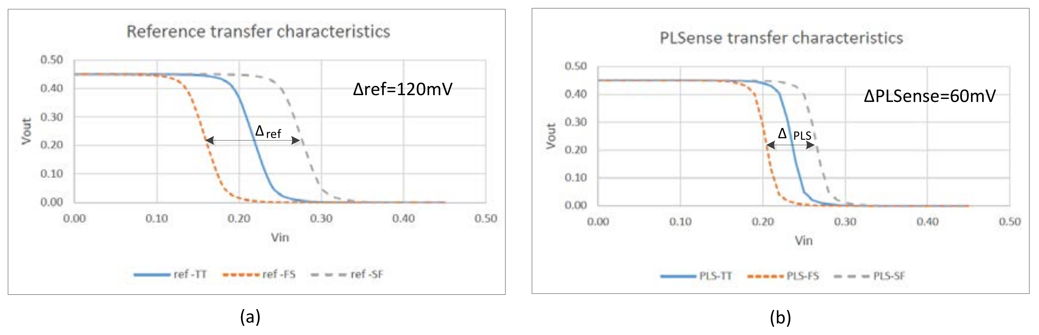
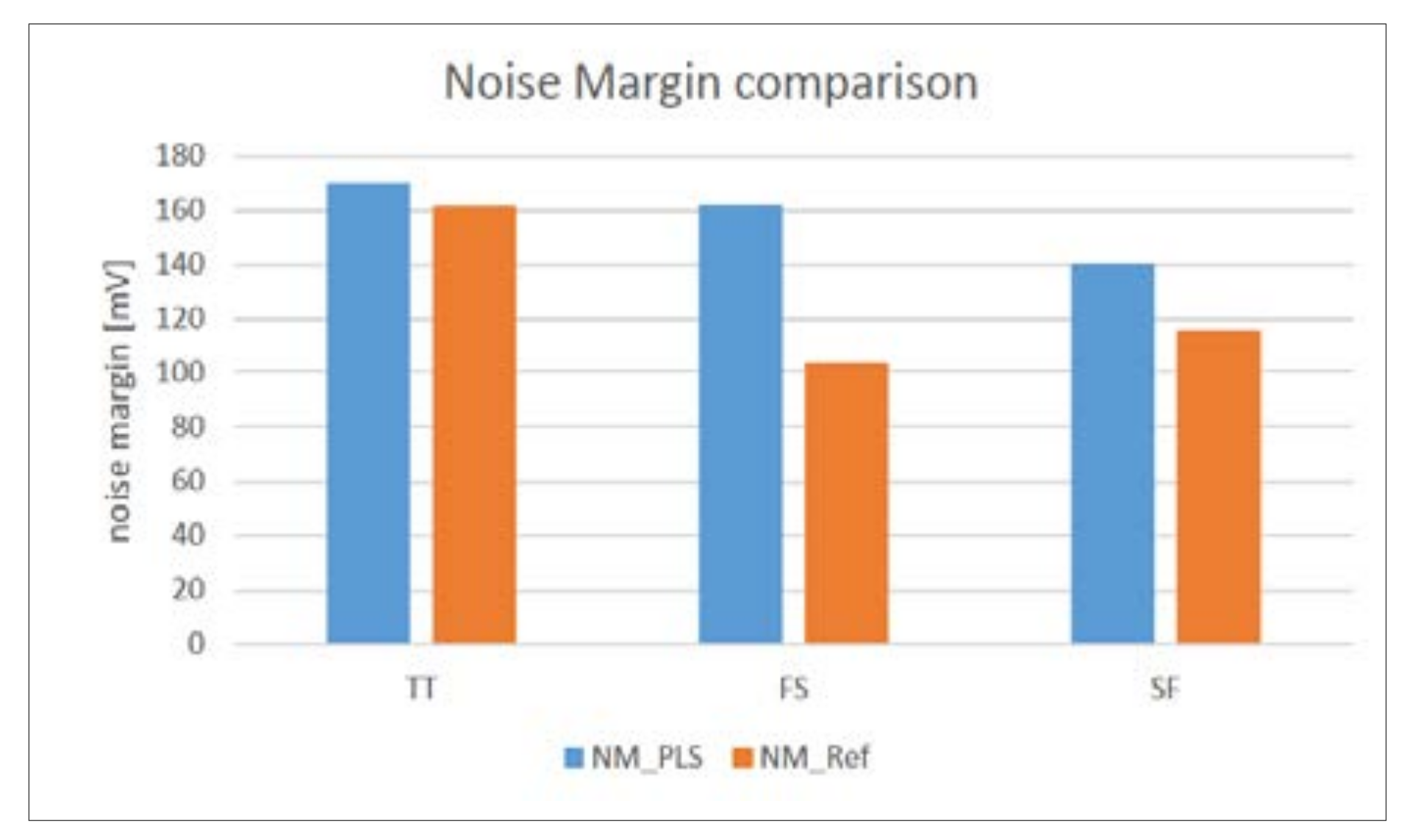
2.1. Low Voltage Libraries Characterization

Low voltage library characterization was one of the first and most important steps in the holistic approach. Utilization of a conventional digital library for low voltage operation is not efficient for many reasons, including high sensitivity to process and temperature variations, non-compatibility of conventional Flip-flops and latches for low voltage operation, lack of mechanisms that allow dynamic adaptation of the gates, and sequential elements to follow real time requirements and environmental conditions and many others. Figure 1 depicts an example of voltage transfer characteristics (VTC) of a conventional standard cell operating from a 450 mV supply voltage under global process variations. As observed in Figure 1, moving from FS to SF corners results in VTC shift of 120 mV. This shift will be even worse, if local (on die) variations are considered, causing a reduced noise margin and reduced reliability. To solve the aforementioned challenges, more than one low voltage libraries were characterized in the frame of this work. Each one of the libraries, comprising approximately 300 digital cells and sequential elements, presented different tradeoffs in terms Vt, size, energy dissipation, minimum supply voltage, and performance. The libraries were used in different modules according to the architectural requirements. The libraries present the following features to address the challenges: (a) mixed threshold (mixed Vt) transistors are utilized. Using transistors with different threshold voltages in different cells and libraries is a known methodology, however, in our case, transistors with different Vts are used inside the same digital cells and sequential elements. The use of mixed Vt transistors (HVT and SVT) in the same cell targets to overcome the relatively slow speed of p-channel transistors and to improve the noise margin (more symmetric VTC) and speed of the cell. To meet certain performance, one can either use a significantly large transistor or use a transistor with a lower Vth (i.e., standard Vth vs. high Vth). In conventional chips, utilization of mixed Vt transistors in a single cell can lead to increased sensitivity to process variations, especially under a low voltage operation. However, the unique Adaptive Dynamic Voltage Control (ADVC) approach, utilized in the proposed MCU SOC, allows reduction of this sensitivity by real time adaptation of the operating voltage, bulk biasing, frequency and other parameters of the systems, according to the process variations and environmental conditions. Mixing different V-th level transistors in the same cell require meeting additional design rules which in some cases require wider space. However, when comparing this to the option of enlarging the transistors, we found that the method of using mixed Vth, provides a better optimization of performance vs. area; (b) most of the cells allow selective bulk biasing for the PMOS transistors; (c) high fan-ins are avoided; (d) flip flop architecture avoid any ratioed logic and (e) careful sizing to assure area-energy-performance-reliability tradeoff.
Figure 1b demonstrates the advantages of the characterized low voltage library over a conventional solution, showing 50% variance reduction. This also results in improved static noise margins, as shown in Figure 2.

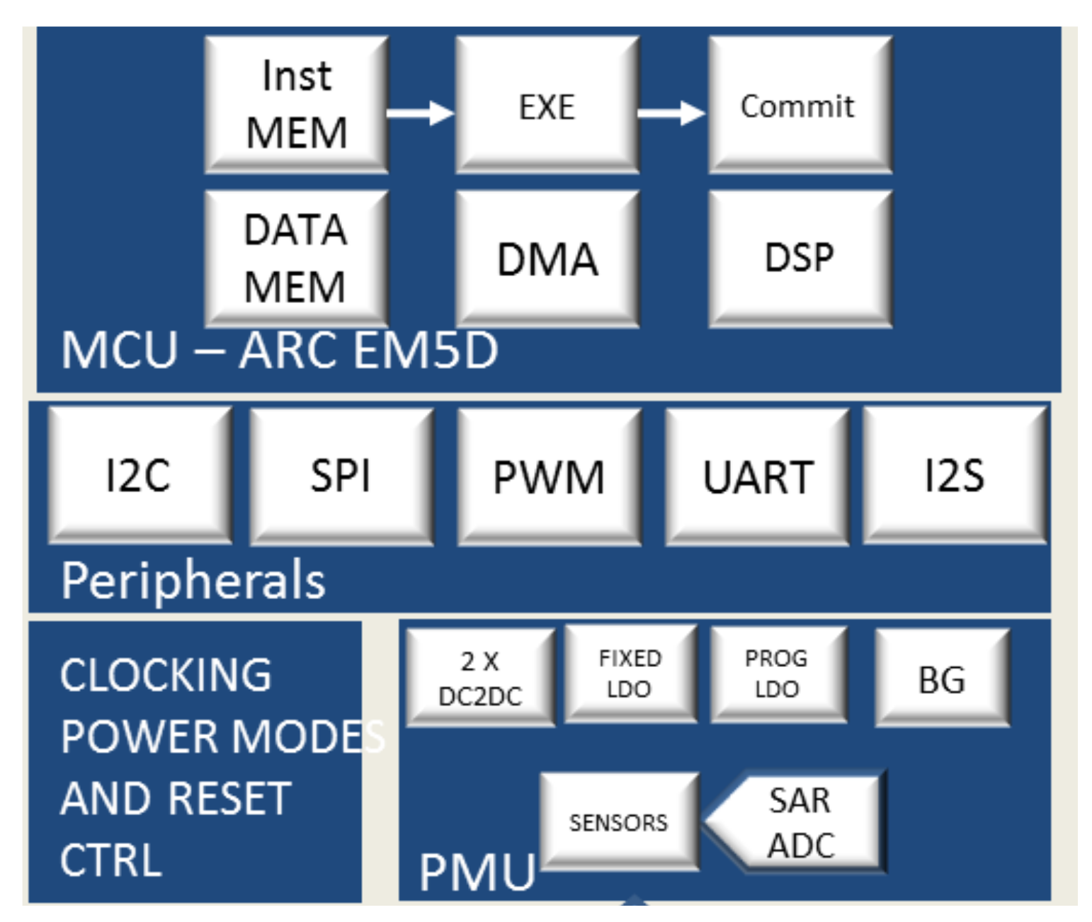
2.2. MCU SoC Architecture

The SoC includes the complete Synopsys ARC EM5D MCU core, featuring a full set of DSP instructions and minimizing energy consumption at a wide range of frequencies: 312 K–80 MHz. It also contains all external interfaces to support the SOC operation, including an “Always-On” function at the system level. The SoC integrates all the needed analog blocks which are required for a complete “Sub/Near-threshold” operation, including programmable DC to DC converters (DC2DC), LDO, ADC, level shifters and other needed components, as shown in Figure 3.
The chip can be connected directly to a battery source and can accept input voltages from 1.6 V up to 3.6 V. The chip also supports an advanced Adaptive Dynamic Voltage Control (ADVC) approach of the internal core and bias voltages change to achieve the best power per performance for the desired speed and given environmental conditions. Furthermore, it improves the production yield and life time of the chip. The SoC chip incorporates a set of embedded memories and an extensive range of on-chip enhanced I/O’s.

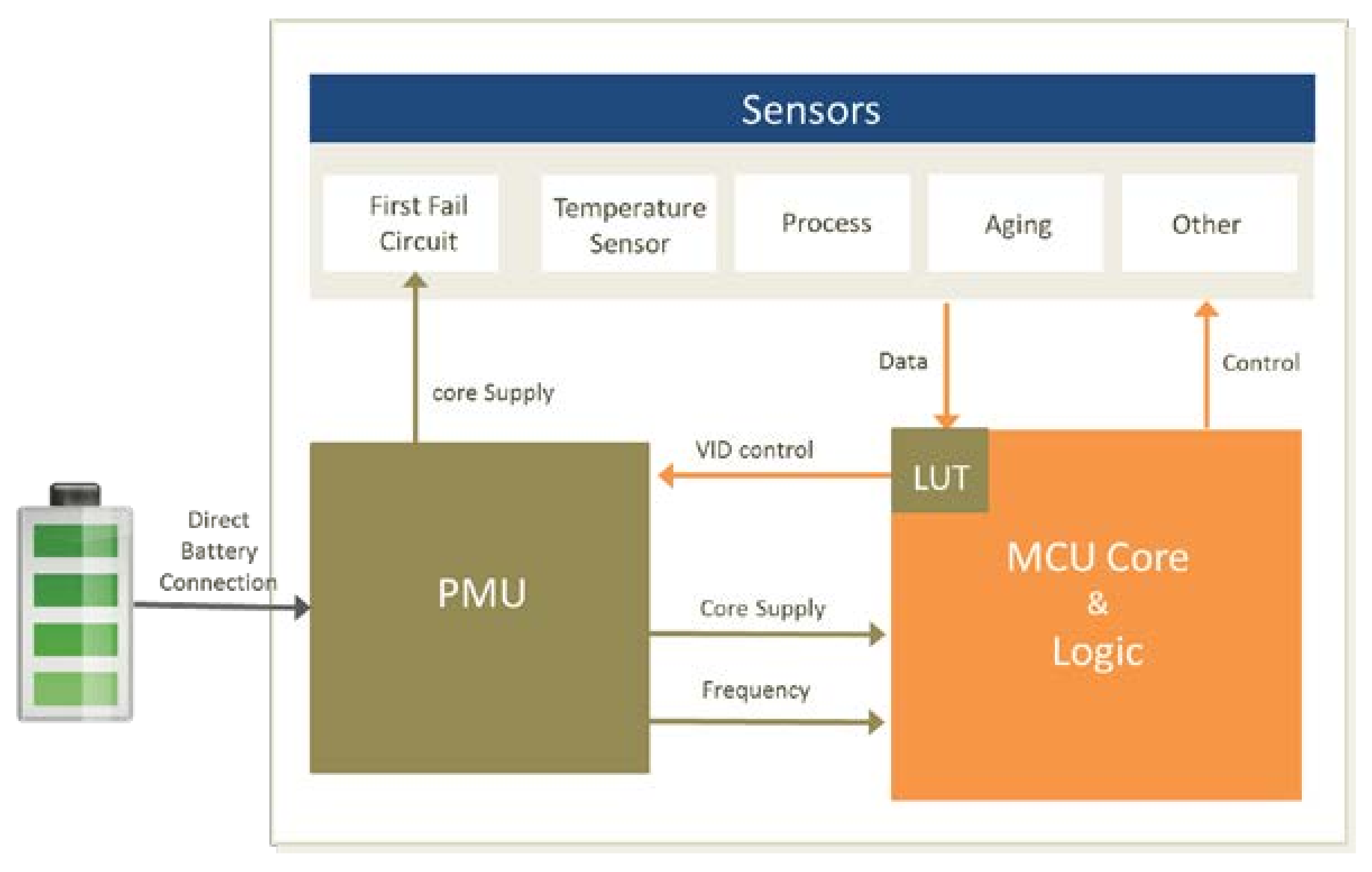
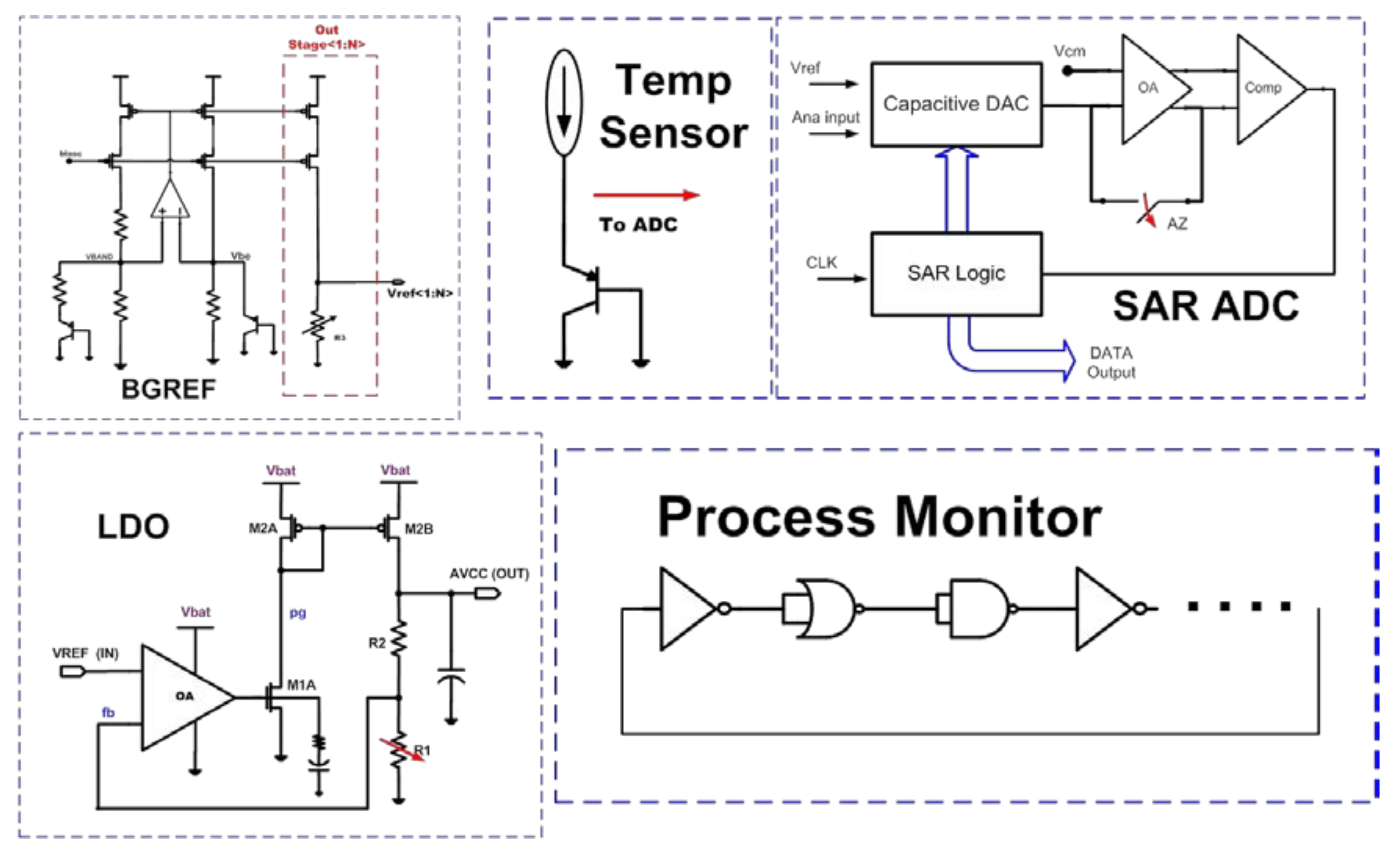
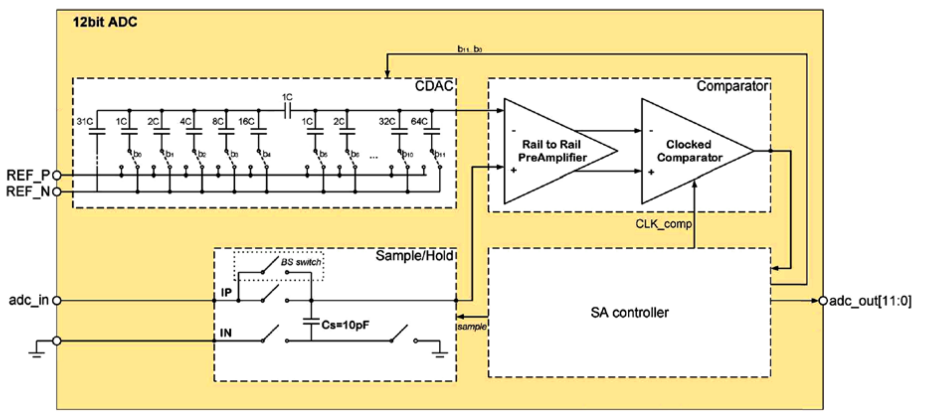
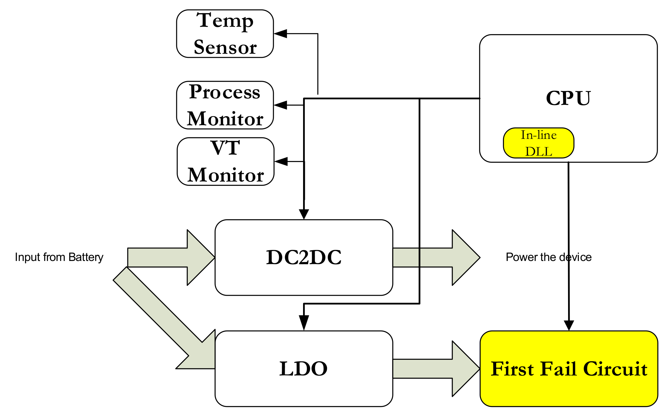
2.3. Adaptive Dynamic Voltage Control (ADVC)

A diagram describing the ADVC feature is shown in Figure 4. The Power Management Unit (PMU) contains switching and linear power supply generators, all of which are connected to the battery. A series of sensors continuously measure the relevant Silicon operating parameters of the IC and feeds this information into a look-up-table (LUT) which sets the voltage identification code (VID) to the PMU. The VID determines the VCC level of the core and a programmable first-fail circuit (Ffail), whose VCC characteristics track those of the core. The user sets the target operating speed, and a built-in SW algorithm controls the core and the bias voltages based on monitored sensors and the data in the LUT. This Adaptive Dynamic Voltage Control (ADVC) continuously optimizes the core voltage to optimize power consumption for any user-selected target frequency and different environment conditions, and also improve the chip yield and reliability. The core voltage can be changed between 0.45 V to 1.1 V in small steps of 10 mv. The sensors include process monitors, temperature sensor, aging sensor, threshold voltage (Vt) sensor, and other sensors.
The PMU contains power supply circuits required for energy efficient operation. There is two inductor based DC to DC converters (DC2DC) which supply separate VCC voltages to the Core at an efficiency above 85% even at low VCC voltages and low load currents. The supplies can operate from near-Vt levels (0.45 V) up to 1.1 V. Figure 5 shows a fixed voltage LDO which provides a 0.9–1.1 V supply to analog and always-on circuits, while the sensors are supplied by a separate dynamically programmable LDO. A current mirror output stage is used in the LDO in order to improve the power supply rejection. The current mirror links the gate of the PMOS driver to VCC, while enables a more constant current even when VCC has AC ripples. The accuracy of all of these circuits is enabled by an on-die Bandgap reference circuit (BGREF), also shown in Figure 5. The PMU has the option of controlling the body bias of the MCU N-wells for Vt variance compensation.
Figure 5 shows several examples of the on-die sensors used to measure the Silicon parameters. These sensors are distributed in several locations on the chip to compensate for on die variations and supply the necessary feedback to the software ADVC algorithm. Temperature is measured by monitoring the Base-Emitter (Vbe) voltage of a parasitic PNP transistor and comparing it to a reference voltage, similar to [45]. The accuracy of this thermal sensor is ±5 °C across the operating range, which is sufficient for this application.
All of the analog parameters are sampled by Successive Approximation Analog-to-Digital Converters (SAR ADC). A more detailed diagram of the SAR ADC is shown in Figure 6 and it is similar to the architecture shown in [46]. It has a coarse and fine split capacitor array, which is divided by an attenuation capacitor to save cap area while maintaining high resolution. It is a pseu-differential 12-bit SAR ADC that is configurable to be used with varying sample rates and 2 resolution options to allow for high resolution, high speed solutions which consume more power as well as low resolution, low speed solutions which consume minimal power. The accuracy of ADC can also be increased by oversampling and the decimation is done by the digital section inside the PLS15 to reach up to 16-bit accuracy. At the high-performance mode, it is capable of a 12 bit, 1 MSPs (1 Mega Sample per second) measurement consuming 410 uW and 0.35 pJ/step. Vbat is used as the reference voltage. An additional 6 bit SAR is available for the low power modes (12 uW @ 1 MSPs). The ADC is capable of a single shot or continuous sampling and has a built-in averaging of multiple samples.
A process monitoring circuit (PM), is utilized to obtain an accurate reading of the SoC’s frequency capability. The PM is comprised of a ring oscillator which uses a variety of standard cells. The first-fail (FFail) circuit is a programmable critical path monitor (CPM) [47] designed to show the lowest acceptable SoC core voltage. The FFail gives a fail signal at a voltage which is slightly higher than the failing SoC voltage at a given frequency. It is designed from elements representing critical paths of the chip and can be digitally and linearly controlled with up to 8 bits. The detailed description of the FFail circuit is presented in the next sub-section.

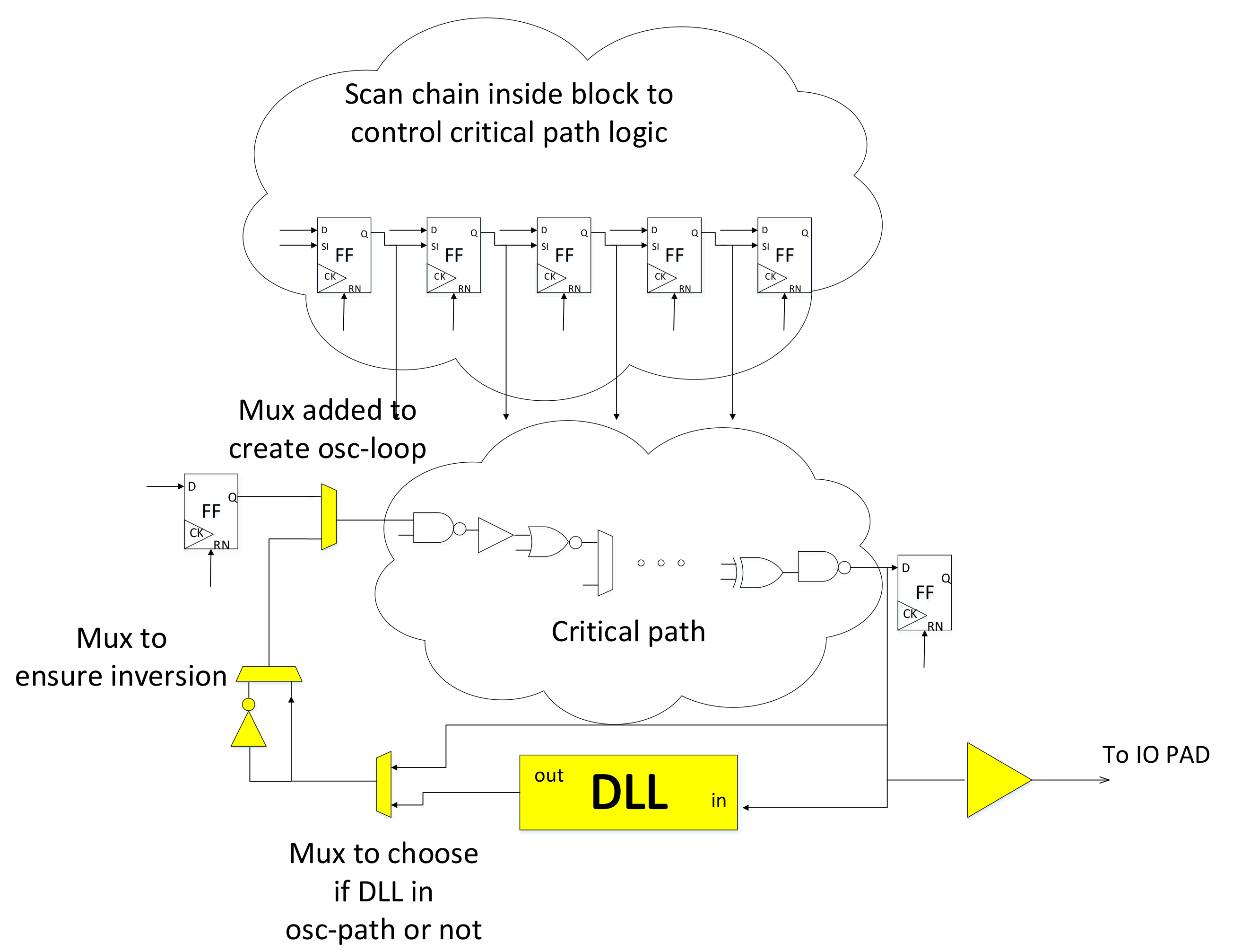
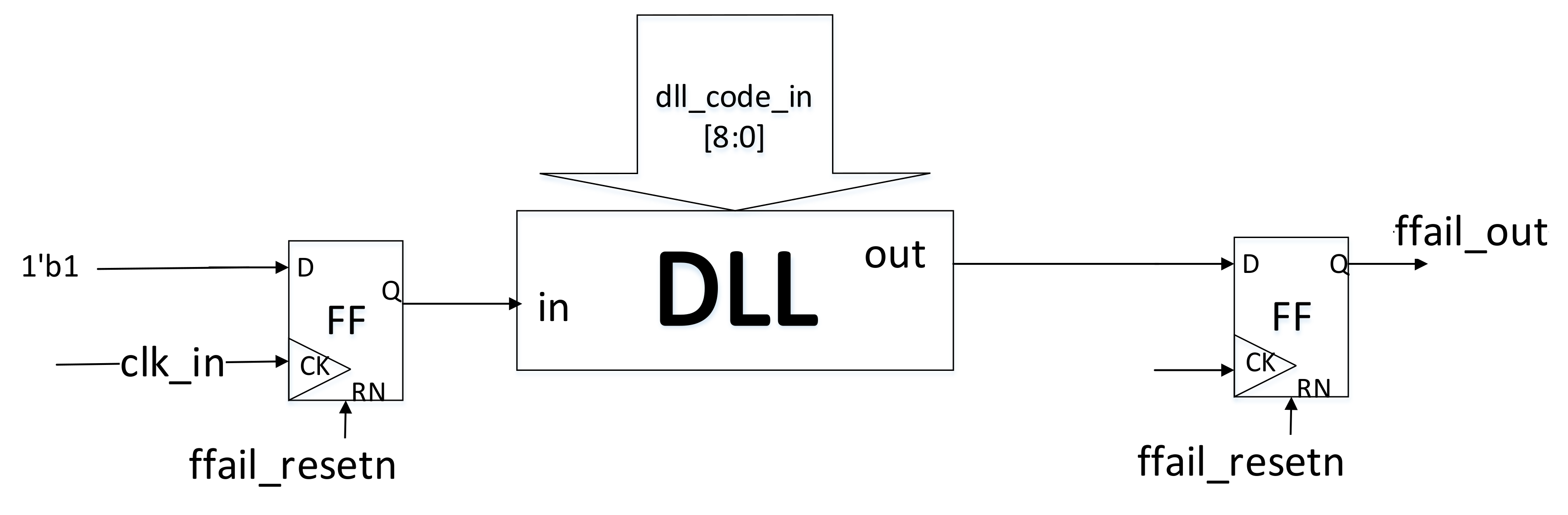
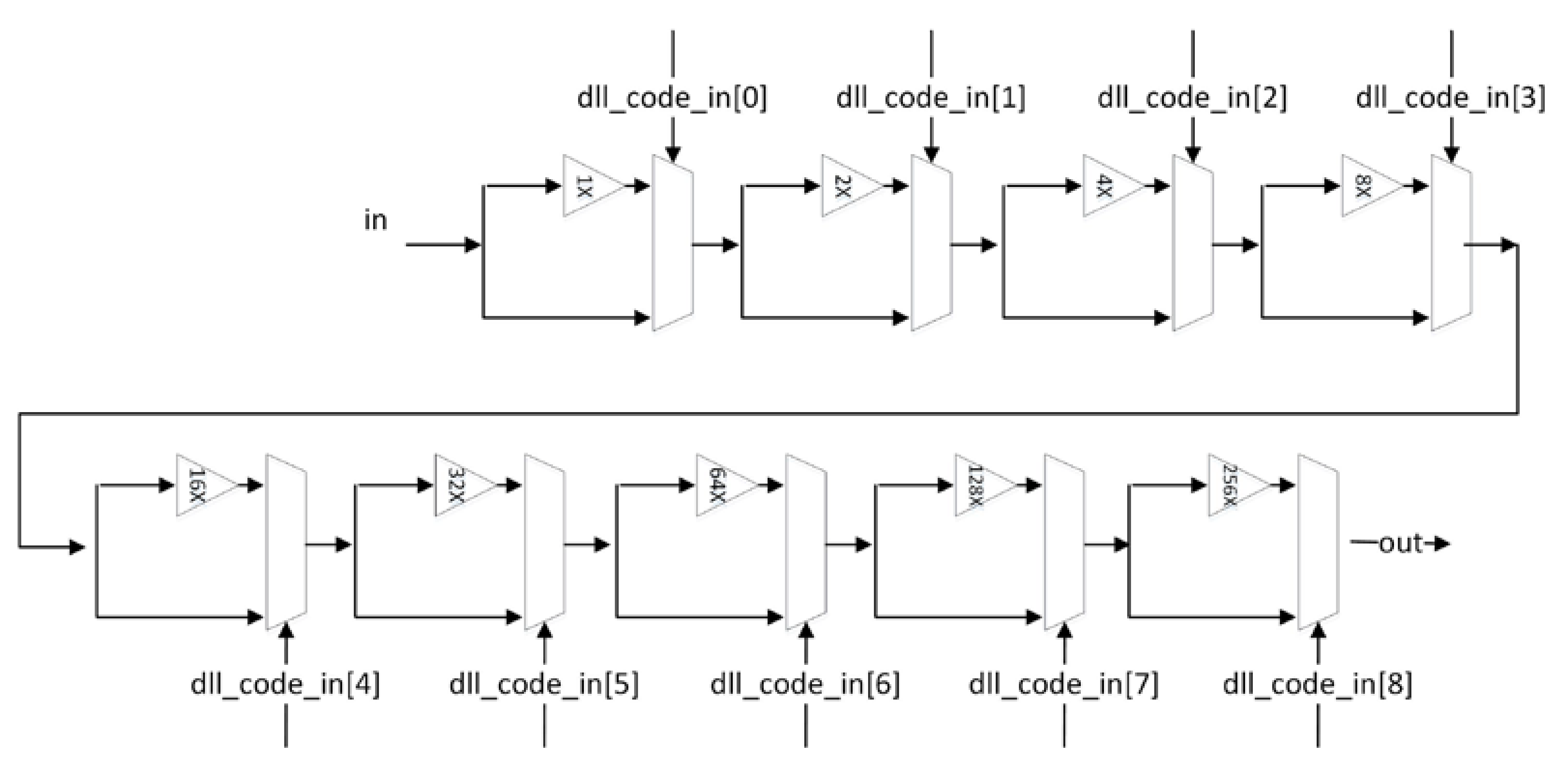
2.3.1. First Fail Circuit
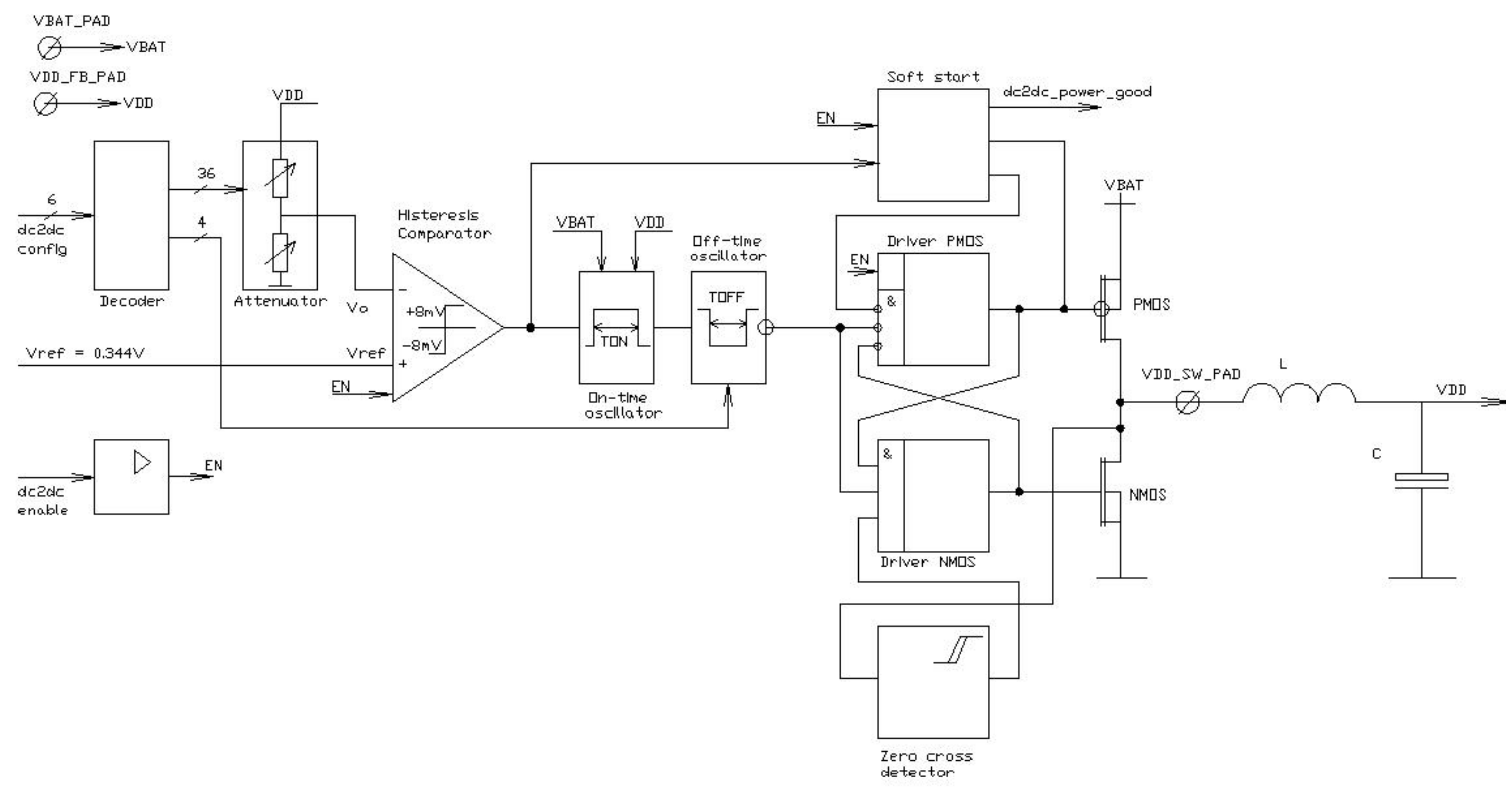
FFail circuit is one of the most important and key components of the proposed system. It is used to determine the optimal operating voltage per device for a required frequency and environment conditions, such as the chip silicon corner or temperature. The FFail employs the exact programmable DLL which is used to represent the accurate delay of the critical path, which represents the worst-case timing path of the system. By using FFail circuit, it is possible to mimic the exact delay of the critical path and with this emulation, it is possible to get an accurate optimal operating voltage. The proposed FFail is unique since the measurement of the critical path delay is done in-line to the critical path logic, and an accurate representation of this path is done using a programmable DLL which is connected to the critical path logic. In the existing solutions, the measurements of the critical path delay are done either externally from the critical path logic or by not being represented using a programmable DLL.
A general architecture of the proposed FFail concept is shown in Figure 7. The structure of the in-line DLL is depicted in Figure 8. A programmable DLL is connected to the output and input of the combinational cells (represent the critical path) in a way which creates an oscillation loop, as seen in Figure 8. The output of the oscillation loop is driven to an external PAD to be sampled by an external frequency measurement tool. Critical path combinational cells can be controlled through existing Flip-Flops in the device, which drives a valid data into each Flip-Flop in order to control the logic of the critical path to ensure that the logic of the selected critical path enables the signal propagation.
To ensure the desired operation, three multiplexers are added within the oscillation path. The first multiplexer is used to bypass the programmable DLL when required. The goal of the second multiplexer is to close the oscillation loop. The third multiplexer is used to add an additional inversion stage if needed to ensure oscillation. By using these three multiplexers with different settings, it is possible to create an oscillation loop through the critical path logic or the critical path logic and the programmable DLL.
The DLL is programed to represent the delay of the critical path delay in the following way. At the first stage, the critical path is configured to assure the data flows through that critical path. The second stage of this method is to set the multiplexer controls so that only the plurality of the critical path combinational cells are closed in an oscillation loop, and the frequency is measured off-chip. The third stage of this method is to set the multiplexer controls so that the programmable DLL is also connected within the oscillation loop, while all DLL control bits are zero and the frequency is again measured off-chip. The fourth stage of this method is to modify the programmable DLL code in a binary search until the output frequency equals half the frequency, which was measured in the second stage (via the combination cells only). The fifth stage of this method is to record the DLL code within a memory element within the device. This code represents the delay of the critical path and will be further used to program the FFail circuit.
The structure of the FFail circuit is shown in Figure 9. The circuit is constructed from the same programmable DLL, which is used in-line with the critical path. The same DLL control code, which was generated using the in-line DLL and the critical path oscillation loop is also used for the FFail programmable DLL. Two Flip-Flops are used within the FFail Circuit. The first Flip-flop drives the input to the programmable DLL and has an input which is always connected to “1”, and the second Flip-Flop which is connected to the output of the programmable DLL. Both Flip-Flops can be reset before the test is performed. Subsequently, exactly two clock cycles are given to both Flip-Flops, after these two clock cycles, the output of the second Flip-Flop is sampled by the CPU. If the result equals ‘1′ then the DLL delay is too short, and if the result equals ‘0′, the DLL delay is too long.
In order to determine the optimal voltage, the operating voltage of the FFail logic, which is controlled by a separate voltage source from the rest of the device, is set to the minimal voltage. For a given frequency, which is given to the clock of the FFail Flip-Flops, a test can be performed to check if the DLL delay is too short or too long at a given voltage. By using this method, the voltage can be increased until a pass result is obtained by the FFail circuit. A pass condition indicates that the FFail delay is exactly within the given clock period. Once this condition is met, the test can be stopped, and the last passing voltage can be used by the rest of the device as the operating voltage. As the FFail circuit has an equal path delay as the worst case critical path within the device, we ensured that the device would function correctly given the same voltage of operation, which is also used by the FFail Circuit.
A more detailed drawing of the DLL circuit is shown in Figure 10. The dll_code_in [8:0] bus determines how many delay elements will be enabled. These are binarily weighted for a total of 511 different delay combinations, which are used to tune the FFail function.

2.3.2. DC2DC

The DC2DC, implemented in this work is optimized for low power applications and maintains high efficiency, even at low load current and low output voltages. In general, switched DC-to_DC conversion can be accomplished by three modes of operation: Pulse-Width Modulation (PWM), Pulse-Frequency Modulation (PFM) and Pulse-Skipping Modulation (PSM—also known as discontinuous mode) (Figure 11). Among the above-mentioned, Pulse Width Modulation (PWM) mode is most appropriate for high power modes, where the switching and conduction losses are relatively small and maximum load current is required. The Pulse-Frequency Modulation (PFM) mode is used when the transmitted power is comparable to the switching losses. Adjusting the frequency limits these switching losses, such that this mode is useful at medium loads. At very low loads, the PSM mode “skips” many of the pulses and generates a pulse only when the voltage drops below a pre-determined threshold, which increases the light-load efficiency. Consequently, the PSM mode is appropriate for low-current loads and was adopted in this design.
Figure 12 shows the schematic implementation of the DC2DC. The configuration of the DC2DC is input through the decoder, a block which operates at 1.1 V. The output voltage, VDD, is determined by the attenuator, which is a resistive voltage divider for the sensed output signal. The divided voltage is compared with the reference voltage, Vref, by the comparator. The comparator features a 4 mV-wide hysteresis loop. The soft start block ensures smooth charging of the output capacitor at power-up. If the signal EN = 0 then the signal power_good = 0. The soft start circuit blocks PMOS Driver and puts the fixed voltage to the gate of the PMOS driver, such that it acts as a current source. When the voltage VDD reaches a predetermined level, the high-level output of the comparator will disable the soft start circuit. The power_good signal is enabled, which allows the normal function of the PMOS driver. The turn-on time of the PMOS driver during normal operation is determined by the On-Time Oscillator according to the following expression:
Ton = L*Ip/(VBAT-VDD)
where L is inductance, Ip is peak current (15 mA), VBAT is battery voltage and VDD is output voltage.
The off-time of the PMOS is determined by the off-time oscillator according to:
Toff = L*Ip/VDD
A zero-cross detector senses when the NMOS current changes direction, at which point the NMOS driver is disabled. Additionally, a second-order L-C filter is connected at the output of the DC2DC to smoothen its output voltage.
Figure 13 shows typically measured efficiency for an input voltage of 3.0 V and an output of 0.8 V. The efficiency is high across 3 orders of magnitude. The DC2DC is capable of driving currents from 1 Ua–10 mA for output voltages of 0.4–1.1 V and input voltages of 1–3.8 V.

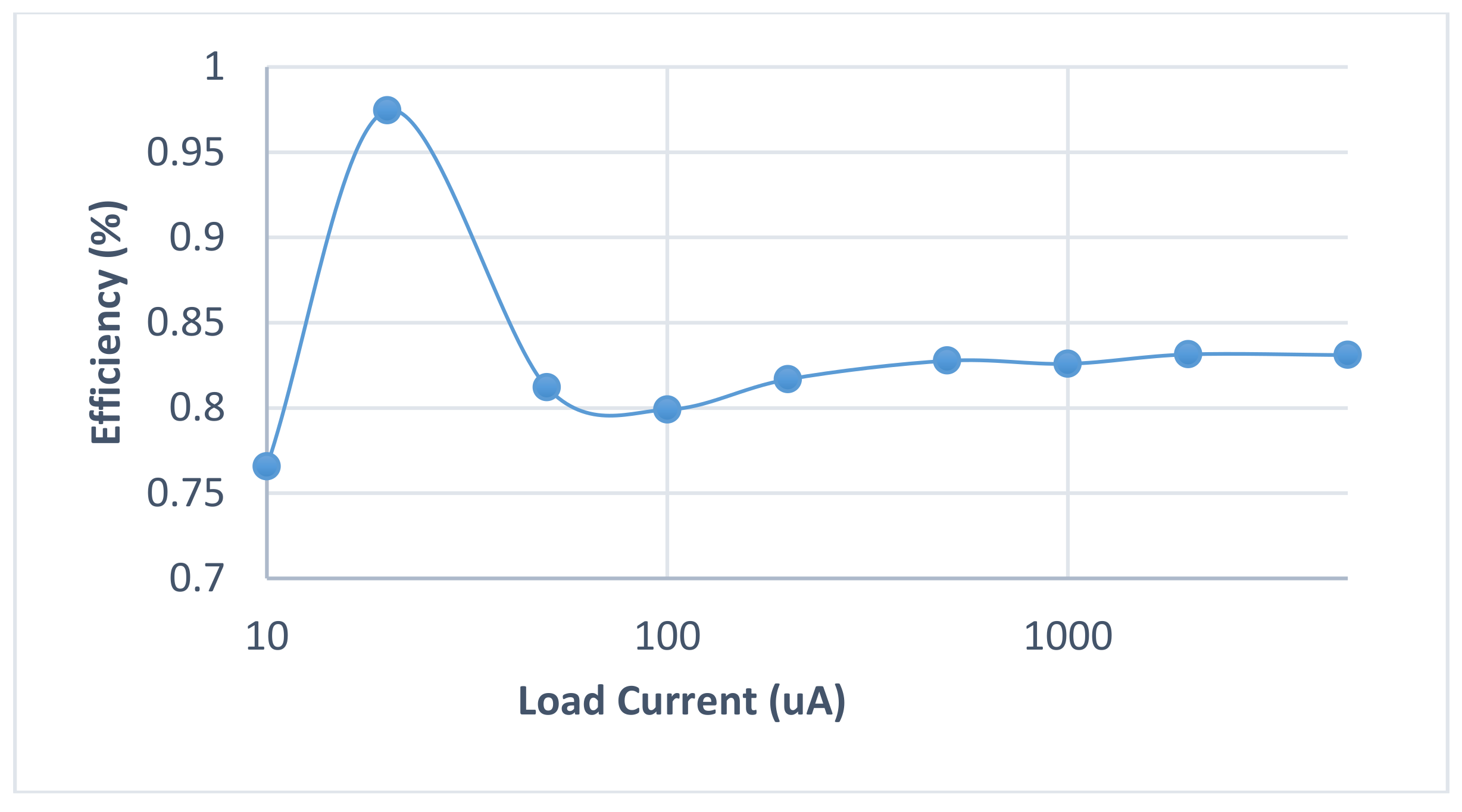
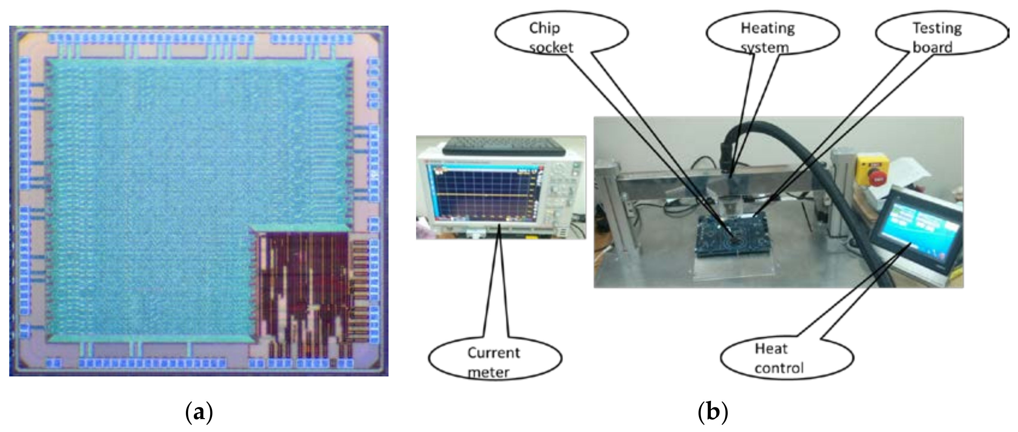
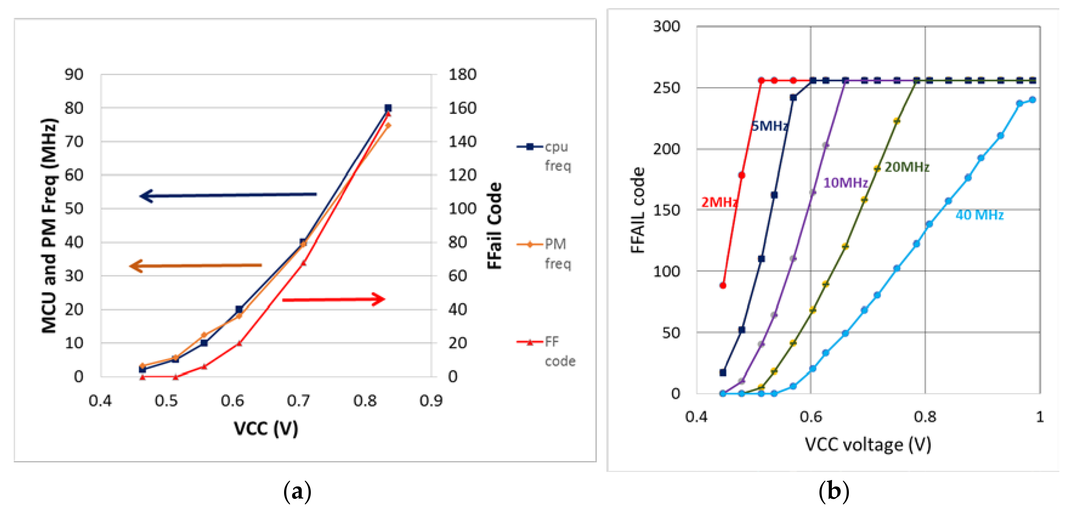
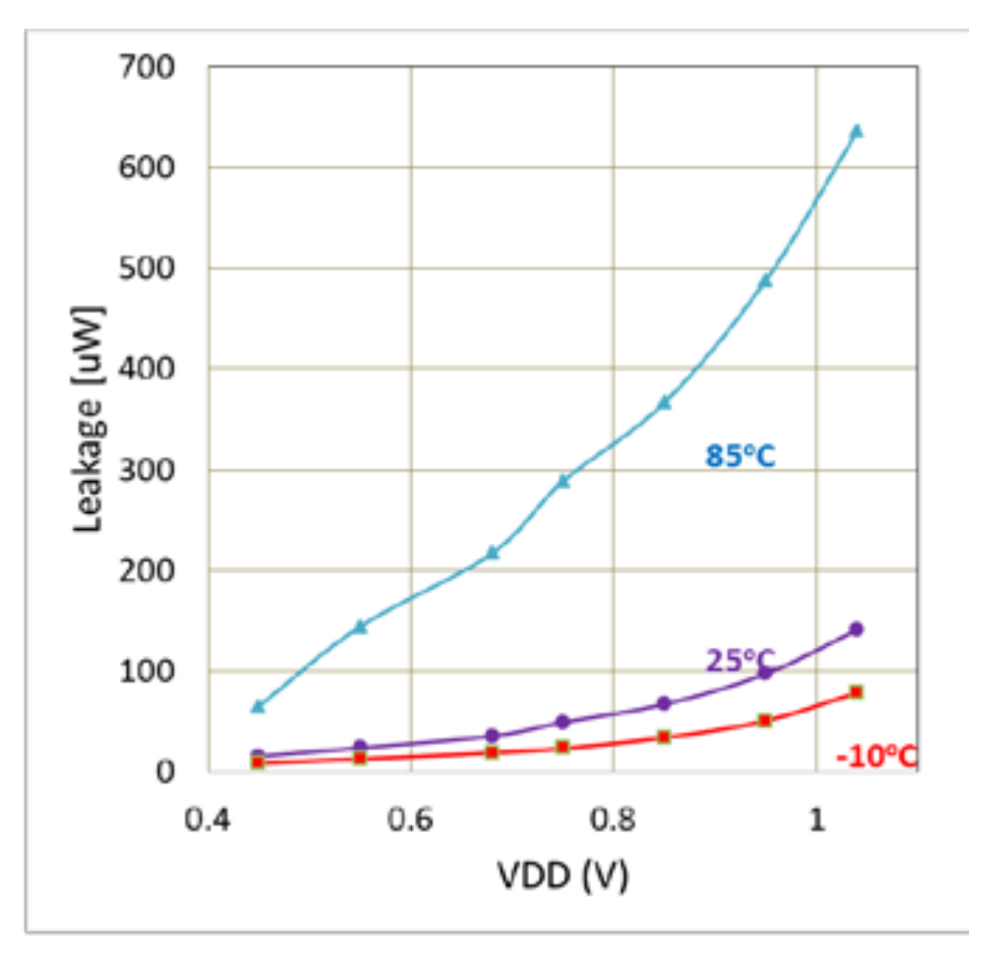
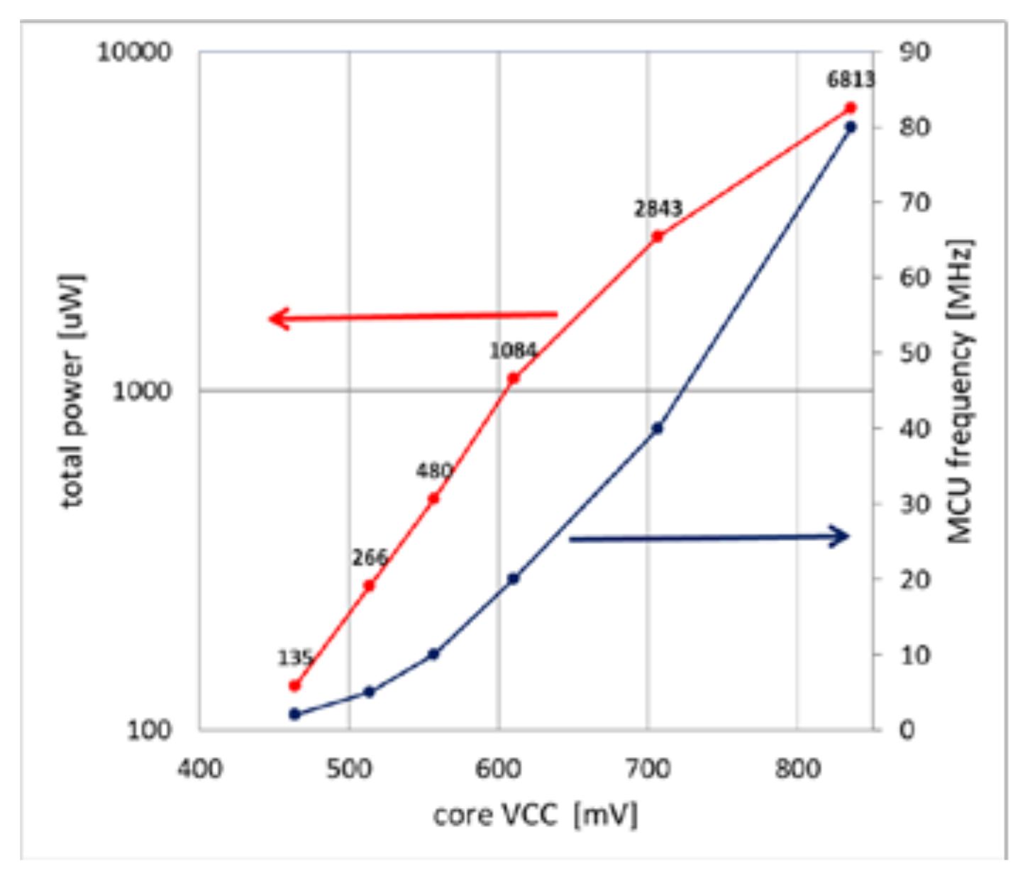
3. Measurements Results

A test chip, dubbed PLS10, consisting of the proposed MPU SoC has been designed and fabricated in TSMC’s 40 nm ULP process (die photo is shown in Figure 14a). The measurement setup is shown in Figure 14b. It includes conventional tools, such dedicated testing board, current meter and heating system. Many units have been characterized at different temperatures, process corners, and voltages.
The measured functionality of the FFail circuit is shown in Figure 15. On the left graph of Figure 15, the Core and PM circuit frequencies are plotted against the supply VCC voltage. The PM circuit is designed such that its frequency is similar to the Core’s. The FFail code (at 40 MHz) is shown on the right axis of the figure. It is shown that the FFail code tracks the Core frequency very accurately, proving its usefulness as a canary-bird circuit to determine the minimum operating voltage. On the right graph of Figure 15, the FFail fail code is plotted against VCC for 5 frequencies. At lower VCC levels, the FFail code shows a nearly linear response to VCC level up to code saturation. Figure 15 indicates good MCU and Ffail functionality down to VCC = 0.45 V at 2 MHz.
The power and performance of the MCU are shown in Figure 16 and Figure 17. The graph shows a power range of 135–6800 μW at frequencies of 2–80 MHz for VCC ranging from 0.45–0.85 V, which includes current for always on. As expected, the leakage power is a strong function of temperature, as shown in Figure 16, but is reduced dramatically with the VCC reduction.
A comparison to state-of-the-art commercial SOCs is shown in Table 1. In order to make an “apples-to-apples” comparison, we listed only Cortex M4F MCUs. Our IC (PLS10) has a 3× improved current/DMIPS (Dhrystone Million Instructions per second) compared to the next best chip. We also showed a 2× improvement in current/MHz, which is a measure of energy efficiency. The table was measured and compared at a nominal 20 MHz but at lower frequencies < 2 MHz and VCC = 0.45–0.5 V, the power difference being 3–4×. We also listed the next generation of our SOC (PLS15). PLS15 is an improved version of the PLS10, which also includes an improved Ffail circuits (the concept was presented in Section 2.3.1), embedded flash memory, 12 bit ADC, LCD controller, real time clock (RTC) operating in the deep subthreshold regime and consuming less than 100 nA.

4. Conclusions

In this paper, an ultra-low power MCU SoC was presented. The SoC Includes the complete Synopsys ARC EM5D core MCU, featuring a full set of DSP instructions and minimizing energy consumption at a wide range of frequencies: 312 K–80 MHz. Detailed descriptions of the design approach, including library characterization, SoC architecture, ADVC mechanism, Ffail and DC2DC circuits were shown. The proposed core allows for operation between 0.45–1.1 V volts, with a direct battery connection for an input voltage of 1.6–3.6 V. Measurement resulting from a PLS10 test chip, designed and fabricated in 40 nm ULP technology, showed that the peak energy efficiency is 18 μW/MHz. A comparison to state-of-the-art commercial SoCs was presented, showing a 3–5× improved current/DMIPS (Dhrystone Million Instructions per second) in comparison to the next best chip. It was shown that the next generation of the SoC is expected to improve these numbers by almost 2×.

Author Contributions

All authors contributed equally to this work.

Funding

We would like to acknowledge Taiwan Semiconductor Manufacturing Company, Ltd. for technical assistance and test chip manufacturing support.

Conflicts of Interest

The authors declare no conflict of interest.

References

  1. Whatmough, P.; Lee, S.K.; Lee, H.; Rama, S.; Brooks, D.; Wei, G. A 28 nm SoC with a 1.2 GHz 568 nJ/prediction sparse deep-neural-network engine with >0.1 timing error rate tolerance for IoT applications. In Proceedings of the IEEE International Solid-State Circuits Conference, San Francisco, CA, USA, 5–9 February 2017. [Google Scholar]
  2. Kuo, F.W.; Ferreira, S.B.; Chen, H.N.R.; Cho, L.-C.; Jou, C.-P.; Hsueh, F.-L.; Madadi, I.; Tohidian, M.; Shahmohammadi, M.; Babaie, M.; et al. A Bluetooth Low-Energy Transceiver With 3.7-mW All-Digital Transmitter, 2.75-mW High-IF Discrete-Time Receiver, and TX/RX Switchable On-Chip Matching Network. IEEE J. Solid-State Circuits 2017, 52, 1144–1162. [Google Scholar] [CrossRef]
  3. Alioto, M. Enabling the Internet of Things: From Integrated Circuits to Integrated Systems; Springer: Berlin/Heidelberg, Germany, 2017. [Google Scholar]
  4. Sarwesh, P.; Shekar, N.; Shet, V.; Chandrasekaran, K. Energy-Efficient Network Architecture for IoT Applications; Springer: Berlin/Heidelberg, Germany, 2017. [Google Scholar]
  5. Bang, S.; Wang, J.; Li, Z.; Gao, C.; Kim, Y.; Dong, Q.; Chen, Y.P.; Fick, L.; Sun, X.; Dreslinski, R.; et al. 14.7 a 288 µw programmable deep-learning processor with 270 kb on-chip weight storage using non-uniform memory hierarchy for mobile intelligence. In Proceedings of the IEEE International Solid-State Circuits Conference, San Francisco, CA, USA, 5–9 February 2017. [Google Scholar]
  6. Gautschi, M.; Schiavone, P.D.; Traber, A.; Loi, I.; Pullini, A.; Rossi, D.; Flamand, E.; Gürkaynak, F.K.; Benini, L. Near-threshold RISC-V core with DSP extensions for scalable IoT endpoint devices. IEEE Trans. Very Large Scale Integr. (VLSI) Syst. 2017, 25, 2700–2713. [Google Scholar] [CrossRef]
  7. Kulkarni, A.; Page, A.; Attaran, N.; Jafari, A.; Malik, M.; Homayoun, H.; Mohsenin, T. An energy-efficient programmable manycore accelerator for personalized biomedical applications. IEEE Trans. Very Large Scale Integr. (VLSI) Syst. 2018, 26, 96–109. [Google Scholar] [CrossRef]
  8. Adegbija, T.; Rogacs, A.; Patel, C.; Gordon-Ross, A. Microprocessor optimizations for the Internet of things: A survey. IEEE Trans. Comput.-Aided Design Integr. Circuits Syst. 2018, 37, 7–20. [Google Scholar] [CrossRef]
  9. Rabaey, J. Low Power Design Essentials; Springer: Berlin/Heidelberg, Germany, 2009. [Google Scholar]
  10. Myers, J.; Savanth, A.; Howard, D.; Gaddh, R.; Prabhat, P.; Flynn, D. 8.1 An 80 nW retention 11.7 pJ/cycle active subthreshold ARM Cortex-M0+ subsystem in 65 nm CMOS for WSN application. In Proceedings of the 2015 IEEE International Solid-State Circuits Conference, San Francisco, CA, USA, 22–26 February 2015. [Google Scholar]
  11. Lim, W.; Lee, I.; Sylvester, D.; Blaauw, D. 8.2 Batteryless Sub-nW Cortex-M0+ processor with dynamic leakage-suppression logic. In Proceedings of the 2015 IEEE International Solid-State Circuits Conference, San Francisco, CA, USA, 22–26 February 2015. [Google Scholar]
  12. Pons, M.; Le, T.; Arm, C.; Severac, D.; Nagel, J.; Morgan, M.; Emery, S. Sub-threshold latch-based icyflex2 32-bit processor with wide supply range operation. In Proceedings of the ESSCIRC Conference European Solid-State Circuits Conference, Lausanne, Switzerland, 12–15 September 2016. [Google Scholar]
  13. Han, J.; Zhang, Y.; Huang, S.; Chen, M.; Zeng, X. An Area-Efficient Error-Resilient Ultralow-Power Subthreshold ECG Processor. IEEE Trans. Circuits Syst. II 2016, 63, 984–988. [Google Scholar] [CrossRef]
  14. Calhoun, B.; Cao, Y.; Li, X.; Mai, K.; Pileggi, L.; Rutenbar, R.; Shepard, K. Digital Circuit Design Challenges and Opportunities in the Era of Nanoscale CMOS. Proc. IEEE 2008, 96, 343–365. [Google Scholar] [CrossRef]
  15. Calhoun, B.; Bolus, J.; Khanna, S.; Jurik, A.; Weaver, A.; Blalock, T. Sub-threshold operation and cross-hierarchy design for ultra low power wearable sensors. In Proceedings of the IEEE International Symposium on Circuits and Systems (ISCAS), Taipei, Taiwan, 24–27 May 2009; pp. 1437–1440. [Google Scholar]
  16. Wang, A.; Calhoun, B.; Chandrakasan, A. Sub-Threshold Design for Ultra-Low-Power Systems; Springer: New York, NY, USA, 2006. [Google Scholar]
  17. Warneke, B.; Pister, K. An ultra-low energy microcontroller for Smart Dust wireless sensor networks. In Proceedings of the IEEE International Solid-State Circuits Conference, San Francisco, CA, USA, 15–19 February 2004; pp. 316–317. [Google Scholar]
  18. Vittoz, E.; Fellrath, J. CMOS analog integrated circuits based on weak inversion operations. IEEE J. Solid-State Circuits 1977, 12, 224–231. [Google Scholar] [CrossRef]
  19. Soeleman, H.; Roy, K. Ultra-low power digital subthreshold logic circuits. In Proceedings of the ACM/IEEE International Symposium on Low Power Electronics and Design, San Diego, CA, USA, 16–17 August 1999; pp. 94–96. [Google Scholar]
  20. Zimmer, B.; Lee, Y.; Puggelli, A.; Kwak, J.; Jevtić, R.; Keller, B.; Bailey, S.; Blagojević, M.; Chiu, P.F.; Le, H.P.; et al. A RISC-V vector processor with simultaneous-switching switched-capacitor DC–DC converters in 28 nm FDSOI. IEEE J. Solid-State Circuits 2016, 51, 930–942. [Google Scholar]
  21. Keller, B.; Cochet, M.; Zimmer, B.; Kwak, J.; Puggelli, A.; Lee, Y.; Blagojević, M.; Bailey, S.; Chiu, P.F.; Dabbelt, P.; Schmidt, C. A risc-v processor soc with integrated power management at submicrosecond timescales in 28 nm fd-soi. IEEE J. Solid-State Circuits 2017, 52, 1863–1875. [Google Scholar] [CrossRef]
  22. Bae, W.; Ju, H.; Park, K.; Han, J.; Jeong, D.K. A Supply-Scalable-Serializing Transmitter with Controllable Output Swing and Equalization for Next-Generation Standards. IEEE Trans. Ind. Electron. 2018, 65, 5979–5989. [Google Scholar] [CrossRef]
  23. Bol, D. Robust and Energy-Efficient Ultra-Low-Voltage Circuit Design under Timing Constraints in 65/45 nm CMOS. J. Low Power Electron. Appl. 2011, 1, 1–19. [Google Scholar] [CrossRef]
  24. Fisher, S.; Teman, A.; Vaysman, D.; Gertsman, A.; Yadid-Pecht, O.; Fish, A. Digital Subthreshold Logic Design—Motivation and Challenges. In Proceedings of the IEEE 25th Convention of Electrical and Electronics Engineers in Israel, Eilat, Israel, 3–5 December 2008; pp. 702–706. [Google Scholar]
  25. Patel, H.N.; Calhoun, B.H.; Mann, R.W. Soft errors: Reliability challenges in energy-constrained ULP body sensor networks applications. In Proceedings of the IEEE 23rd International Symposium on On-Line Testing and Robust System Design (IOLTS), Thessaloniki, Greece, 3–5 July 2017; pp. 209–210. [Google Scholar]
  26. Datta, A.; Ramakrishna, M.; Verma, S.; Joginapally, S. Tutorial T9: Devices and Circuits to Address the Challenges in IOT. In Proceedings of the 30th International Conference on InVLSI Design and 2017 16th IEEE International Conference on Embedded Systems (VLSID), Hyderabad, India, 7–11 Janurary 2017. [Google Scholar]
  27. Jain, S.; Khare, S.; Yada, S.; Ambili, V.; Salihundam, P.; Ramani, S.; Muthukumar, S. A 280mV-to-1.2V Wide-Operating-Range IA-32 Processor in 32 nm CMOS. In Proceedings of the IEEE International Solid-State Circuits Conference, San Francisco, CA, USA, 19–23 February 2012; pp. 66–68. [Google Scholar]
  28. Beigné, E.; Valentian, A.; Miro-Pamades, I.; Wilson, R.; Flatresse, P.; Abouzeid, F.; Benoist, T.; Bernand, C.; Billoint, O.; Clerc, S.; et al. A 460 MHz at 397 mV, 2.6 GHz at 1.3 V, 32 bits VLIW DSP Embedding FMAX Tracking. IEEE J. Solid State Circuits 2015, 50, 125–136. [Google Scholar] [CrossRef]
  29. Zangi, U.; Feldman, N.; Shor, J.; Fish, A. 0.45 v and 18 μA/MHz MCU SOC with Advanced Adaptive Dynamic Voltage Control (ADVC). In Proceedings of the 2017 IEEE S3S Conference, Burlingame, CA, USA, 16–19 October 2017. [Google Scholar]
  30. Li, B.; Hashimoto, M.; Schlichtmann, U. From Process Variations to Reliability: A Survey of Timing of Digital Circuits in the Nanometer Era. IPSJ Trans. Syst. LSI Design Methodol. 2018, 11, 2–15. [Google Scholar] [CrossRef]
  31. Samal, S.K.; Chen, G.; Lim, S.K. Improving performance under process and voltage variations in near-threshold computing using 3D ICs. ACM J. Emerg. Technol. Comput. Syst. (JETC) 2017, 13, 59. [Google Scholar] [CrossRef]
  32. Sarfraz, K.; He, J.; Chan, M. A 140-mV Variation-Tolerant Deep Sub-Threshold SRAM in 65-nm CMOS. IEEE J. Solid-State Circuits 2017, 52, 2215–2220. [Google Scholar] [CrossRef]
  33. Kwong, J.; Ramadass, Y.; Verma, N.; Chandrakasan, A. A 65 nm sub-Vt microcontroller with integrated SRAM and switched capacitor DC-DC converter. IEEE J. Solid-State Circuits 2009, 44, 115–126. [Google Scholar] [CrossRef]
  34. Sridhara, S.; DiRenzo, M.; Lingam, S.; Lee, S.J.; Blazquez, R.; Maxey, J.; Ghanem, S.; Lee, Y.H.; Abdallah, R.; Singh, P.; et al. Microwatt embedded processor platform for medical system-on-chip applications. In Proceedings of the 2010 IEEE Symposium on VLSI Circuits (VLSIC), Honolulu, HI, USA, 16–18 June 2010; pp. 15–16. [Google Scholar]
  35. Sadollahi, M.; Hamashita, K.; Sobue, K.; Temes, G.C. An 11-Bit 250-nW 10-kS/s SAR ADC with Doubled Input Range for Biomedical Applications. IEEE Trans. Circuits Syst. I Regul. Pap. 2018, 65, 61–73. [Google Scholar] [CrossRef]
  36. Chen, C.; Chen, L.; Wang, X.; Zhang, F. A 0.6 V, 8.4 uW AFE circuit for biomedical signal recording. Microelectron. J. 2018, 75, 105–112. [Google Scholar] [CrossRef]
  37. Chen, G.; Fojtik, M.; Kim, D.; Fick, D.; Park, J.; Seok, M.; Chen, M.T.; Foo, Z.; Sylvester, D.; Blaauw, D. Millimeter-scale nearly perpetual sensor system with stacked battery and solar cells. In Proceedings of the 2010 IEEE International Solid-State Circuits Conference, San Francisco, CA, USA, 7–11 February 2010; pp. 288–289. [Google Scholar]
  38. Zhai, B.; Nazhandali, L.; Olson, J.; Reeves, A.; Minuth, M.; Helfand, R.; Pant, S.; Blaauw, D.; Austin, T. A 2.60 pJ/Inst Subthreshold Sensor Processor for Optimal Energy Efficiency. In Proceedings of the 2006 IEEE Symposium on VLSI Circuits (VLSIC), Honolulu, HI, USA, 15–17 June 2006. [Google Scholar]
  39. Gao, H.; Matters-Kammerer, M.; Milosevic, D.; Baltus, P.G. Batteryless mm-Wave Wireless Sensors; Springer: Berlin/Heidelberg, Germany, 2018. [Google Scholar]
  40. Zarate-Roldan, J.; Abuellil, A.; Elsayed, O.; Hussien, F.A.L.; Eladawy, A.; Sánchez-Sinencio, E. 0.2-nJ/b Fast Start-Up Ultralow Power Wireless Transmitter for IoT Applications. IEEE Trans. Microw. Theory Tech. 2018, 66, 259–272. [Google Scholar] [CrossRef]
  41. Sze, V.; Chandrakasan, A. A 0.4-V UWB baseband processor. In Proceedings of the 2007 ACM/IEEE International Symposium on Low Power Electronics and Design, Portland, OR, USA, 27–29 August 2007; pp. 262–267. [Google Scholar]
  42. Sze, V.; Finchelstein, D.; Sinangil, M.; Chandrakasan, A. A 0.7-V 1.8-mW H.264/AVC 720p Video Decoder. IEEE J. Solid-State Circuits 2009, 44, 2943–2956. [Google Scholar] [CrossRef]
  43. Pu, Y.; Pineda de Gyvez, J.; Corporaal, H.; Ha, Y. An Ultra-Low-Energy Multi-Standard JPEG Co-Processor in 65 nm CMOS With Sub/Near Threshold Supply Voltage. IEEE J. Solid-State Circuits 2010, 45, 668–680. [Google Scholar] [CrossRef]
  44. Hocquet, C.; Kamel, D.; Regazzoni, F.; Legat, J.D.; Flandre, D.; Bol, D.; Standaert, F.-X. Harvesting the potential of nano-CMOS for lightweight cryptography: An ultra-low-voltage 65 nm AES coprocessor for passive RFID tags. J. Cryptogr. Eng. 2011, 1, 79–86. [Google Scholar] [CrossRef]
  45. Shor, J.; Luria, K. Miniaturized BJT-Based Thermal Sensor for Microprocessors in 32-and 22-nm Technologies. IEEE J. Solid State Circuits 2013, 48, 2860–2867. [Google Scholar] [CrossRef]
  46. Lyu, T.; Yao, S.; Nie, K.; Xu, J. A 12-Bit High-Speed Column-Parallel Two-Step Single-Slope Analog-to-Digital Converter (ADC) for CMOS Image Sensors. Sensors 2014, 14, 21603–21625. [Google Scholar] [CrossRef] [PubMed]
  47. Zangi, U.; Feldman, N. In Line Critical Path Delay Measurement for Accurate Timing Indication for a First Fail Mechanism. U.S. Patent 9,882,564, 30 January 2018. [Google Scholar]
  48. MSP432P401R, MSP432P401M SimpleLink™ Mixed-Signal Microcontrollers. Available online: http://www.ti.com/lit/ds/slas826g/slas826g.pdf (accessed on 6 April 2018).
  49. Very Low Drop Voltage Regulator with Inhibit Function. Available online: http://www.st.com/resource/en/datasheet/cd00000546.pdf (accessed on 6 April 2018).
  50. ATSAM ARM-based Flash MCU SAM4L Series. Available online: http://ww1.microchip.com/downloads/en/DeviceDoc/Atmel-42023-ARM-Microcontroller-ATSAM4L-Low-Power-LCD_Datasheet.pdf (accessed on 6 April 2018).
  51. Apollo Datasheet, Ultra-Low Power MCU Family. Available online: https://www.eembc.org/ulpmark/Apollo_MCU_Data_SheetDS0010V0p90.pdf (accessed on 6 April 2018).
Figure 1. Voltage transfer characteristics of (a) Regular (reference) standard cell and (b) The characterized standard cell with 50% variance reduction.
Jlpea 08 00014 g001
Figure 2. Comparing the proposed and conventional (reference) solutions to noise margins.
Jlpea 08 00014 g002
Figure 3. SOC Block Diagram including full MCU sub-system, clock generation unit and Power Management Unit (PMU).
Jlpea 08 00014 g003
Figure 4. The ADVC features an interaction between the PMU, LUT and the on-die sensors.
Jlpea 08 00014 g004
Figure 5. Simplified schematics of some of the circuits used in the PMU.
Jlpea 08 00014 g005
Figure 6. Diagram of the SAR ADC.
Jlpea 08 00014 g006
Figure 7. A general architecture of the FFail circuit which utilizes the in-line DLL.
Jlpea 08 00014 g007
Figure 8. The scheme of the in-line DLL. The yellow elements represent modules that were added to the original design.
Jlpea 08 00014 g008
Figure 9. The structure of the FFail circuit.
Jlpea 08 00014 g009
Figure 10. The structure of the DLL circuit.
Jlpea 08 00014 g010
Figure 11. The three modes of the DC2DC operation.
Jlpea 08 00014 g011
Figure 12. Schematic of the DC2DC.
Jlpea 08 00014 g012
Figure 13. Measured efficiency vs. load current for Vin = 3 V and Vout = 0.8 V.
Jlpea 08 00014 g013
Figure 14. (a) Die Photo, (b) Measurements setup.
Jlpea 08 00014 g014
Figure 15. (a) measured correlation between the FFail circuit code (at 40 MHz) and the MCU and PM frequencies at 25oC; (b) Measured FFail code vs. voltage for frequencies between 2–40 MHz.
Jlpea 08 00014 g015
Figure 16. Leakage power of the SOC vs. VCC for different temperatures.
Jlpea 08 00014 g016
Figure 17. Power and performance of the SOC vs. Core VCC at room temperature.
Jlpea 08 00014 g017
Table 1. Power/performance metrics compared to other commercial Cortex Cores (Running Dhrystone 2.1 at 20 MHz). The performance numbers were taken from commercial data-sheets.
ChipMCUDMIPS/MHzCurrent/DMIPSOptimal Current per MHz on VBAT at 3 V [uj]
TI MSP432P401x [48]32 bit Cortex M4F1.276.491.6 uA/MHz
STM43L433xx [49]32 bit Cortex M4F1.279.295 uA/MHz
ATMEL SAM4L [50]32bit Cortex M4F1.2147.5177 uA/MHz
Ambiq Apollo [51]32 bit Cortex M4F1.229.235 uA/MHz
This Work
(PLS10)
32 bit EM5D (equivalent to Cortex M4F)1.810.3318.6 uA/MHz
This Work
(PLS15)
32 bit EM5D1.85.5510 uA/MHz

