Article

SOTB Implementation of a Field Programmable Gate Array with Fine-Grained Vt Programmability †

1
Electroinformatics Group, Nanoelectronics Research Institute, National Institute of Advanced Industrial Science and Technology (AIST), 1-1-1 Umezono, Tsukuba, Ibaraki 305-8568, Japan
2
Department of Information and Computer Science, College of Engineering, Kanazawa Institute of Technology, 7-1 Ohgigaoka, Nonoichi, Ishikawa 921-8501, Japan
3
Computer Science Course, Fundamental Science and Technology, Graduate School of Science and Technology, Meiji University, 1-1-1 Higashi-Mita, Tama-ku, Kawasaki-shi, Kanagawa 214-8571, Japan
*
Author to whom correspondence should be addressed.
This is an extended version of paper that was presented at the IEEE S3S Conference 2013.
J. Low Power Electron. Appl. 2014, 4(3), 188-200; https://doi.org/10.3390/jlpea4030188
Submission received: 28 February 2014 / Revised: 28 May 2014 / Accepted: 25 June 2014 / Published: 15 July 2014
(This article belongs to the Special Issue Selected Papers from IEEE S3S Conference 2013)

Abstract

:
Field programmable gate arrays (FPGAs) are one of the most widespread reconfigurable devices in which various functions can be implemented by storing circuit connection information and logic values into configuration memories. One of the most important issues in the modern FPGA is the reduction of its static leakage power consumption. Flex Power FPGA, which has been proposed to overcome this problem, uses a body biasing technique to implement the fine-grained threshold voltage (Vt) programmability in the FPGA. A low-Vt state can be assigned only to the component circuits along the critical path of the application design mapped on the FPGA, so that the static leakage power consumption can be reduced drastically. Flex Power FPGA is an important application target for the SOTB (silicon on thin buried oxide) device, which features a wide-range body biasing ability and the high sensitivity of Vt variation by body biasing, resulting in a drastic subthreshold leakage current reduction caused by static leakage power. In this paper, the Flex Power FPGA test chip is fabricated in SOTB technology, and the functional test and performance evaluation of a mapped 32-bit binary counter circuit are performed successfully. As a result, a three orders of magnitude static leakage reduction with a bias range of 2.1 V demonstrates the excellent Vt controllability of the SOTB transistors, and the 1.2 V bias difference achieves a 50× leakage reduction without degrading speed.

1. Introduction

Field programmable gate arrays (FPGAs) are one of the most widespread reconfigurable devices in which various functions can be implemented by storing circuit connection information and logic values into configuration memories. By this reconfigurability, various applications, such as prototyping, automotive, consumer products, mobile devices, industrial equipment, military equipment, aerospace applications, video/picture processing and telecommunication, can be performed on FPGAs. Another attractive point of FPGA is that the logic implementation on FPGAs needs no mask production for front-end design in ASICs. The system embedding FPGAs, promising an overall lower non-recurring engineering (NRE) cost, has cost benefits in comparison with ASIC-based systems. Moreover, FPGAs can be fabricated by advanced semiconductor process technologies, resulting in the reduction of chip costs and the improvement of device performance by rapidly shrinking the silicon die area, because FPGAs ensure a high-volume production capability, due to the implementability of many types of applications. However, the silicon area of FPGAs becomes lager than that of ASICs generally because FPGAs integrate many silicon resources, e.g., programmable interconnects, logic elements and configuration memories, to maintain the feasibility of many types of applications. While the increase of the silicon area, which lengthens interconnection wires, reduces the operating speed of mapped circuits on FPGAs, longer interconnection wires consume more dynamic power. This is one of the reasons why FPGAs are applied to advanced semiconductor process technologies aggressively.
One of the most important issues in the modern FPGA is the reduction of its static leakage power consumption [1]. Static leakage is a serious problem in FPGAs, partly because of the rich and redundant circuit resources provided for flexible programmability and partly because of the lack of a multi-threshold voltage (Vt) optimization capability for the sake of its field-programmability. Previously, techniques to reduce the static leakage current in FPGAs were aggressively examined. It is shown in [2] that the look-up-table (LUT) leakage is reduced by setting a higher threshold voltage (Vt) to static random access memories (SRAMs). In [3], various low-leakage techniques, such as redundant SRAM design, dual Vt design, body biasing and gate biasing, are evaluated. As described in [4], cutting off the power supply of an unused region by sleep transistors aims at reducing the logic slice leakage, which occupies 45% of the total leakage in their FPGA, while the assignment of a higher Vt to the configuration SRAM reduces 98% of the SRAM leakage, while increasing the configuration time by 20%. A routing switch in [5] can reduce the leakage current by 40% and 61% in low-power mode and sleep mode, respectively. The interconnection with fine-grained power-gating technique reduces the total power by 38% in [6]. It is shown in [7] that the heterogeneous routing architecture reduces standby power by 33% without any area penalty and at the cost of less than a 5% performance degradation. A standby power reduction by 99% by using low-leakage memories and the power-gating technique is presented in [8]. On the other hand, our Flex Power FPGA technique [9] uses a body biasing technique to implement the fine-grained programmability of the Vt of the FPGA building block circuits, such as LUT and multiplexer (MUX). A low-Vt state is assigned only to the building blocks along the critical path of the user application design based on the analysis of the design, while the high-Vt state is assigned to the greater part of the FPGA. As a result, a drastic reduction of the static power consumption can be expected. The key factors to attain good static leakage power reduction performance are: (1) a higher sensitivity of the Vt in the transistor to the back gate bias; (2) a fine grain size of the Vt control domain; and (3) the nature of the critical path of the application design.
The SOTB (silicon on thin buried oxide) transistor [10] has an excellent Vt controllability. Compared with the bulk MOS transistor, a wider variation range of the threshold voltage is promised in principle, because it is formed using a thinner buried oxide under a lightly-doped and fully-depleted body region. The SOTB structure is ideal for Flex Power FPGA to attain better static power reduction performance than bulk technology.
After the development of generations of the conventional bulk transistor implementation of Flex Power FPGA test chips [11], the SOTB version of the Flex Power FPGA test chip is fabricated, and its functional test and performance evaluation are performed successfully by mapping the 32-bit binary counter circuit on the test chip. This paper is organized as follows. Section 2 gives overviews of the SOTB and Flex Power FPGA architecture. In Section 3, evaluation results of the operating speed, static leakage current and area-overhead in the fabricated chip are shown. Finally, in Section 4, this paper is concluded.

2. Overviews of the SOTB Transistor and Flex Power FPGA Architecture

2.1. Silicon on Thin Buried Oxide (SOTB) Transistor
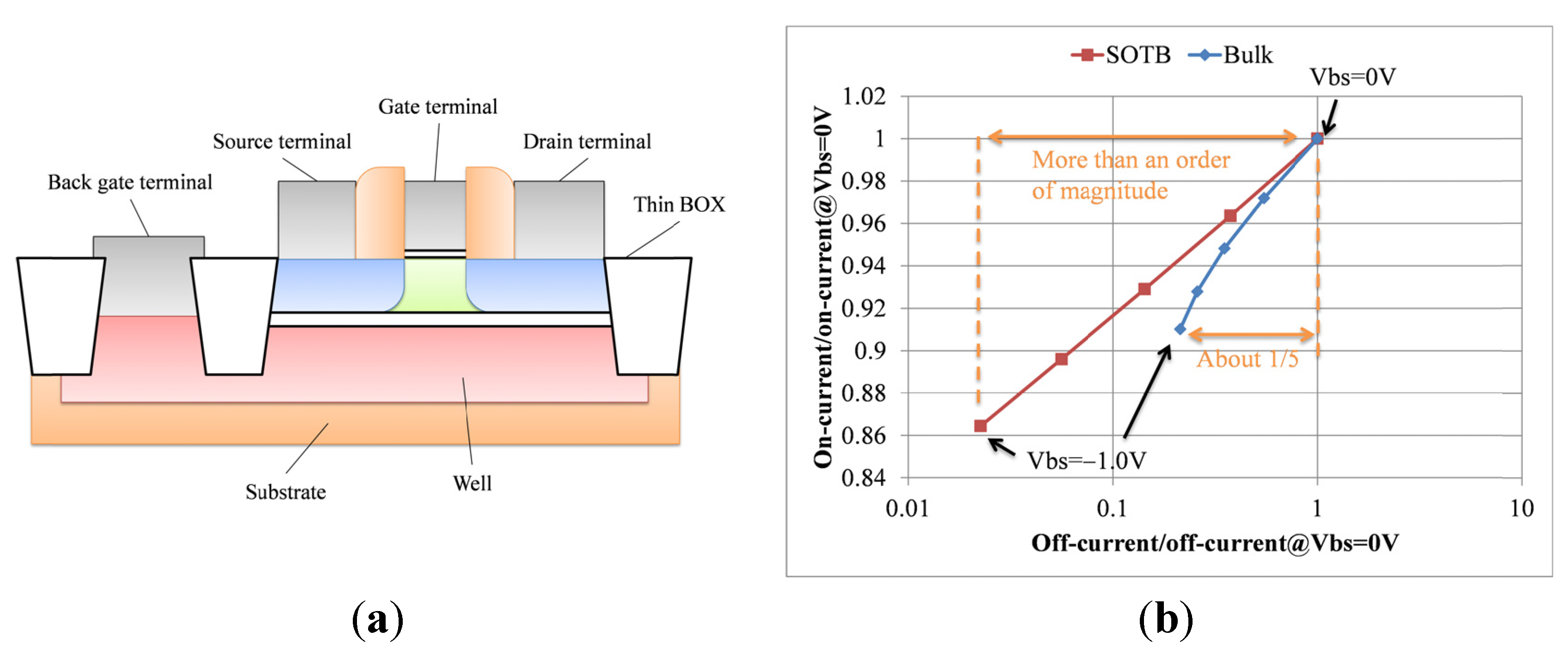
SOTB transistors, as shown in Figure 1a, have some advantages compared with the bulk MOS transistors. SOTB transistors allow a wide back-bias control range for low-power and high-performance applications, because a thinner buried oxide under the lightly-doped and fully-depleted body region is formed as an SOI structure. As a result, by applying this to the SRAM cells, the static noise margins (SNMs) are improved by adding back feedback from the back gate to the front gate [10]. Moreover, SOTB has the smallest threshold voltage variability among bulk MOS, due to its low-dose channel [12].
Figure 1b shows the SPICE simulation results of on-currents and off-currents to the back-bias voltage for the range from 0 V to −1.0 V in a bulk NMOS transistor and an SOTB NMOS transistor in 65-nm technology. Each on-current value is normalized by the on-current value in the case that a back-bias voltage of 0 V is applied. The same manner holds for off-currents. The off-current of the SOTB transistor shifts more than an order of magnitude by applying −1 V to the back gate, while that of the bulk MOS transistor reduces by about 1/5 in the same condition as the SOTB transistor. The on-current variation of the SOTB transistor is also larger than that of the bulk MOS transistor. These results show that the SOTB transistor has a higher sensitivity for the threshold voltage by back gate biasing compared with the bulk MOS transistor, and further, static power reduction efficiency can be expected by applying SOTB transistors to ICs.
Figure 1. (a) The structure of the silicon on thin BOX (SOTB) transistor; and (b) SPICE simulation results of on- and off-currents in a bulk MOS transistor and an SOTB transistor.
Jlpea 04 00188 g001

2.2. Flex Power FPGA Architecture
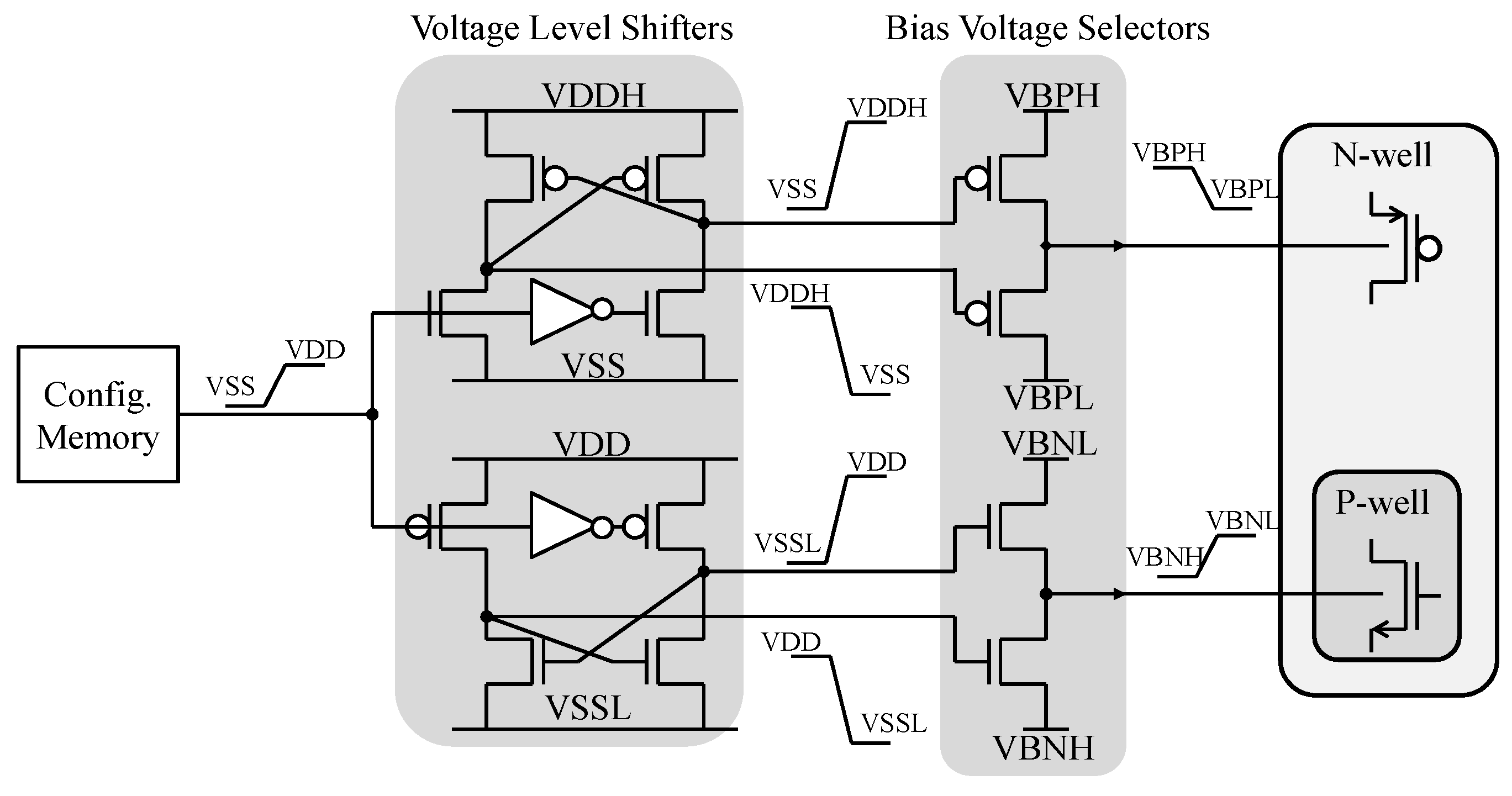
Figure 2 shows the die photo of the SOTB version test chip and the FPGA tile. The test chip described here is a direct conversion from the latest test chip fabricated in 90-nm bulk CMOS technology [11] to the 65-nm SOTB technology. The test chip has a typical island-style FPGA structure with 11 × 11 FPGA tiles. An FPGA tile is connected to other tiles on the left, right, top and bottom of itself via wire segments, which span only four FPGA tiles.
Figure 2. Die photo of (a) the test chip and (b) the FPGA tile.
Jlpea 04 00188 g002
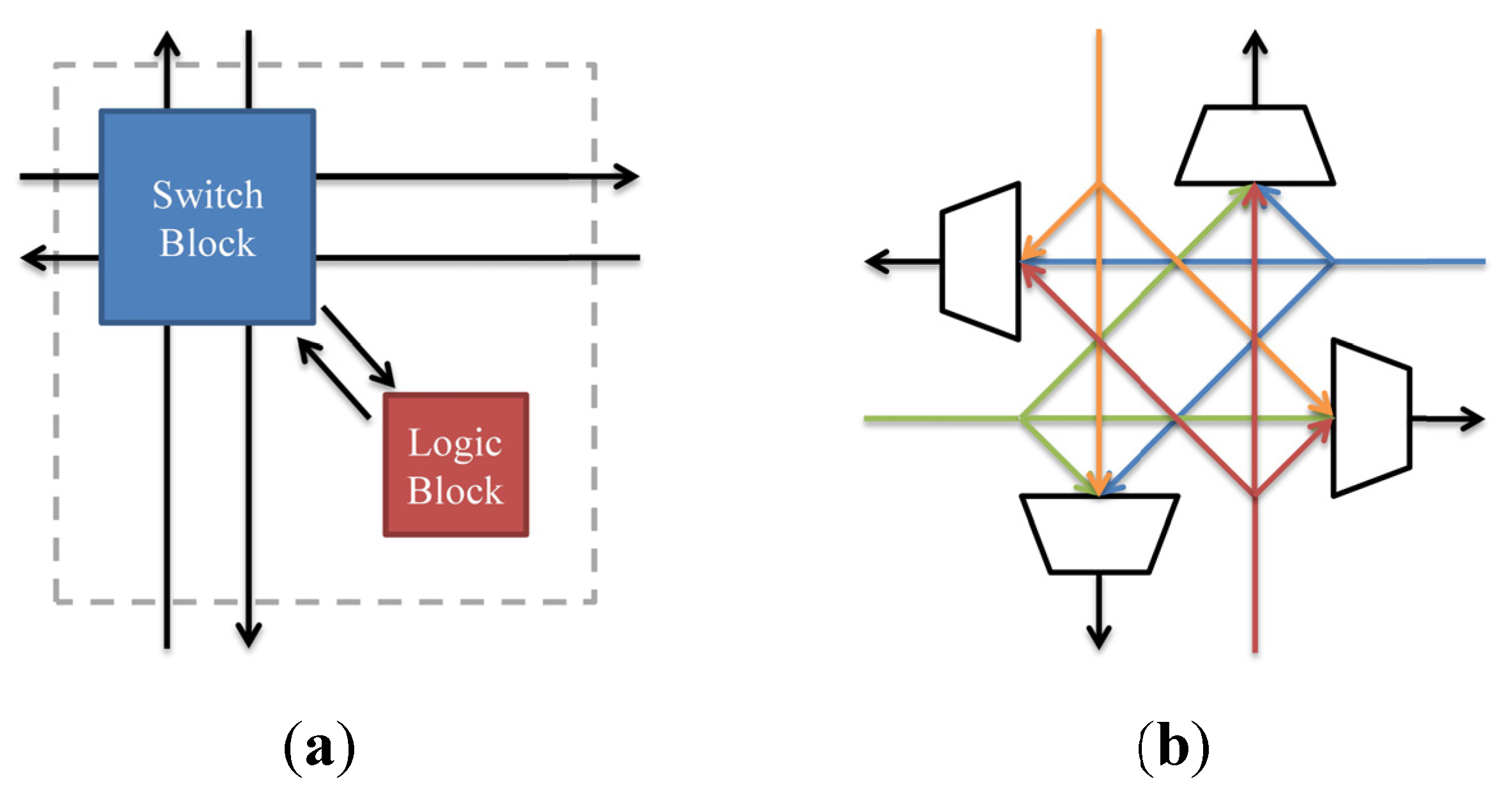
Figure 3a shows the FPGA tile architecture. An FPGA tile has two circuit blocks, a switch block and a logic block. Switch matrixes, input multiplexers (IMUX) and local multiplexers (LMUX), for interconnection of a logic block and a switch block, are contained in the switch block. The switch matrix in the switch block is illustrated in Figure 3b. The switch matrix can interconnect wire segments in the four directions. A signal from one direction can be propagated selectively to the other three directions by switch multiplexers (SMUX), depicted as four trapezoid symbols in Figure 3b.
Figure 3. (a) FPGA tile architecture; (b) Switch matrix in the switch block.
Jlpea 04 00188 g003
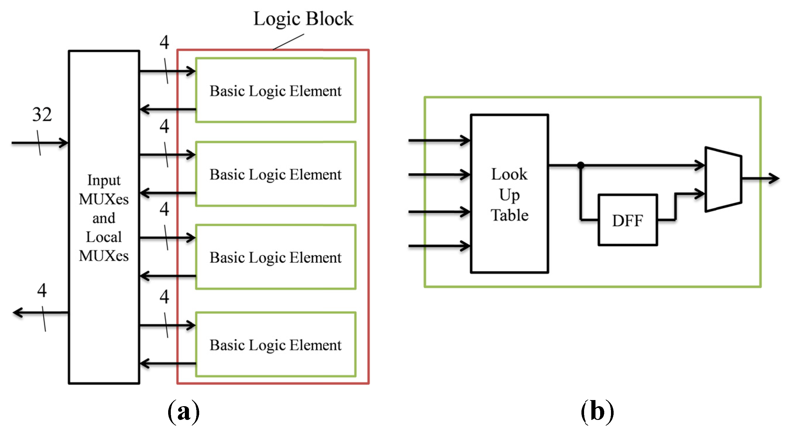
Figure 4a shows the block diagram of a logic block, which is often called a configurable logic block or CLB. A logic block includes IMUXs, LMUXs and four basic logic elements (BLE). IMUXs select 12 signals from signals on the 32 wire segments, and LMUXs input four signals to each basic logic element after selecting from 12 signals as outputs of the IMUXs. The outputs of basic logic elements connect to the switch matrix directly, while these can be fed back via local multiplexers to the inputs of the basic logic elements. Figure 4b depicts a basic logic element. The basic logic element comprises a look-up-table (LUT), a d-flip-flop (DFF) and a 2:1 multiplexer (2:1 MUX). The look-up-table has four inputs and an output. The basic logic element outputs an LUT output signal asynchronously or synchronously via d-flip-flop, which is selected by a 2:1 multiplexer.
Figure 4. (a) Logic block architecture; (b) Basic logic element. MUX, multiplexer; DFF, d-flip-flop.
Jlpea 04 00188 g004
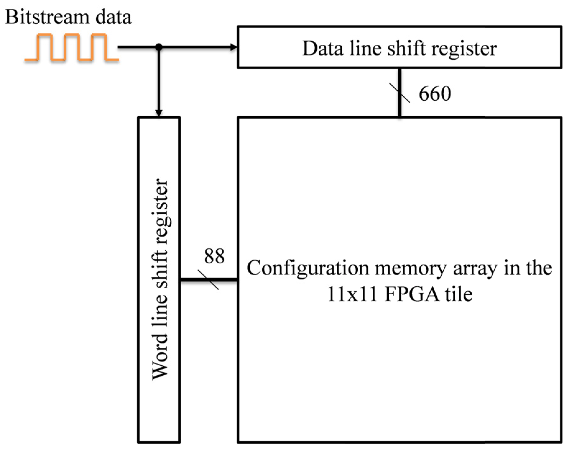
All of the routing through the MUXs and all of the logic functions of the LUTs are defined by the contents of the configuration memories in the FPGA. Figure 5 shows the configuration memory system of the Flex Power FPGA. A word line shift register for the word line strobe and a data line shift register for loading the row by row configuration data are placed on the left side and upper side of the configuration memory array, respectively. A user application design is converted to the configuration information in the bit stream format and is downloaded to the FPGA. The number of word lines is 88, and the number of data lines is 660. Each tile uses 358 configuration bits to represent logic functions, routing and Vt mapping, so that the total number of configuration bits in our test chip is 43,318.
Figure 5. Configuration memory system of the 11 × 11 Flex Power FPGA tile.
Jlpea 04 00188 g005
For each FPGA building block, such as the LUT and MUX, the associated Vt configuration memory bit and body bias control circuit, shown in Figure 6, are provided. Four different bias voltages (VBNL, VBPL, VBNH and VBPH for low-threshold voltage (LVT)/high-threshold voltage (HVT) to NMOS/PMOS) are supplied from the external voltage sources, and the content of the Vt configuration memory bit controls the Vt state (i.e., LVT or HVT) of the corresponding building block circuit by selecting the appropriate bias voltages. As each substrate of the FPGA building block is separated by the triple-well structure, which plays the role of the back gate, individual control of the Vt in FPGA building blocks can be done by the programmable body bias control circuit.
Figure 6. Programmable body bias control circuit. VBPH, voltage bias for high-threshold voltage to PMOS; VBPL, voltage bias for low-threshold voltage to PMOS; VBNL, voltage bias for low-threshold voltage to NMOS; VBNH, voltage bias for high-threshold voltage to NMOS.
Jlpea 04 00188 g006
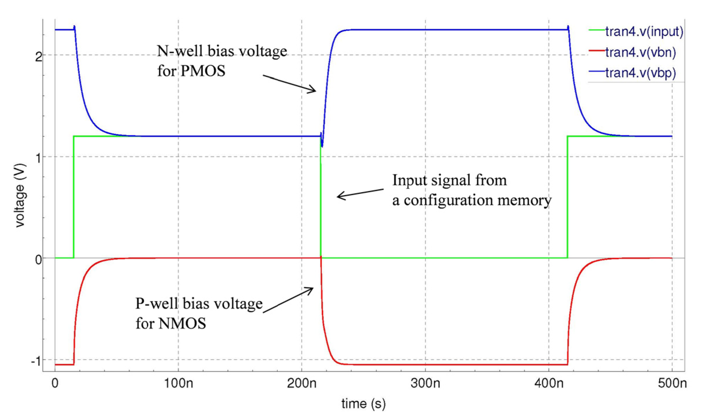
Figure 7 shows the SPICE simulation result of the programmable body bias control circuit. The blue (upper), green (middle) and red (lower) waveforms on the figure show the input signal from a configuration memory along with the resulting n-well bias voltage for PMOS and p-well bias voltage for NMOS. The green line, blue line and red line indicate the signal from a configuration memory, n-well bias voltage for PMOS and p-well bias voltage for NMOS, respectively. When the signal from a configuration memory is 1.2 V, 1.2 V and 0 V are applied to the n-well of PMOS and the p-well of NMOS, respectively, resulting in lower Vt conditions for PMOS and NMOS. In the case that the signal from a configuration memory is 0 V, the body bias control circuit outputs 2.15 V for the n-well and −1.05 V for the p-well. A higher Vt is assigned to PMOS and NMOS.
Figure 7. SPICE simulation results of the programmable body bias control circuit.
Jlpea 04 00188 g007
The grain size of the Vt control domains is set to extremely fine, i.e., multiplexer level, in order to fully demonstrate the maximum power reduction performance of Flex Power FPGA. The number of the Vt control domains in a tile is 57, and the total number in the test chip reaches 6897 bits of the Vt configuration memory. Programmable body bias control circuits, as well as well separation areas are the overheads for the fine-grained Vt control, which will be optimized in the later versions. The FPGA architecture in the test chip is summarized in Table 1.
Table 1. Summary of the FPGA architecture. BLE, basic logic elements; Vt, threshold voltage.
ParameterValue
# of tiles121 (11 × 11)
Wire length4
Switch matrix topologyDisjoint
Routing architectureUnidirectional and single driver programmable interconnect
Routing channel width16
# of BLEs per a CLB (configurable logic block)4
# of CLB inputs13
# of CLB outputs4
# of BLE inputs7
# of Vt control domains per a tile57
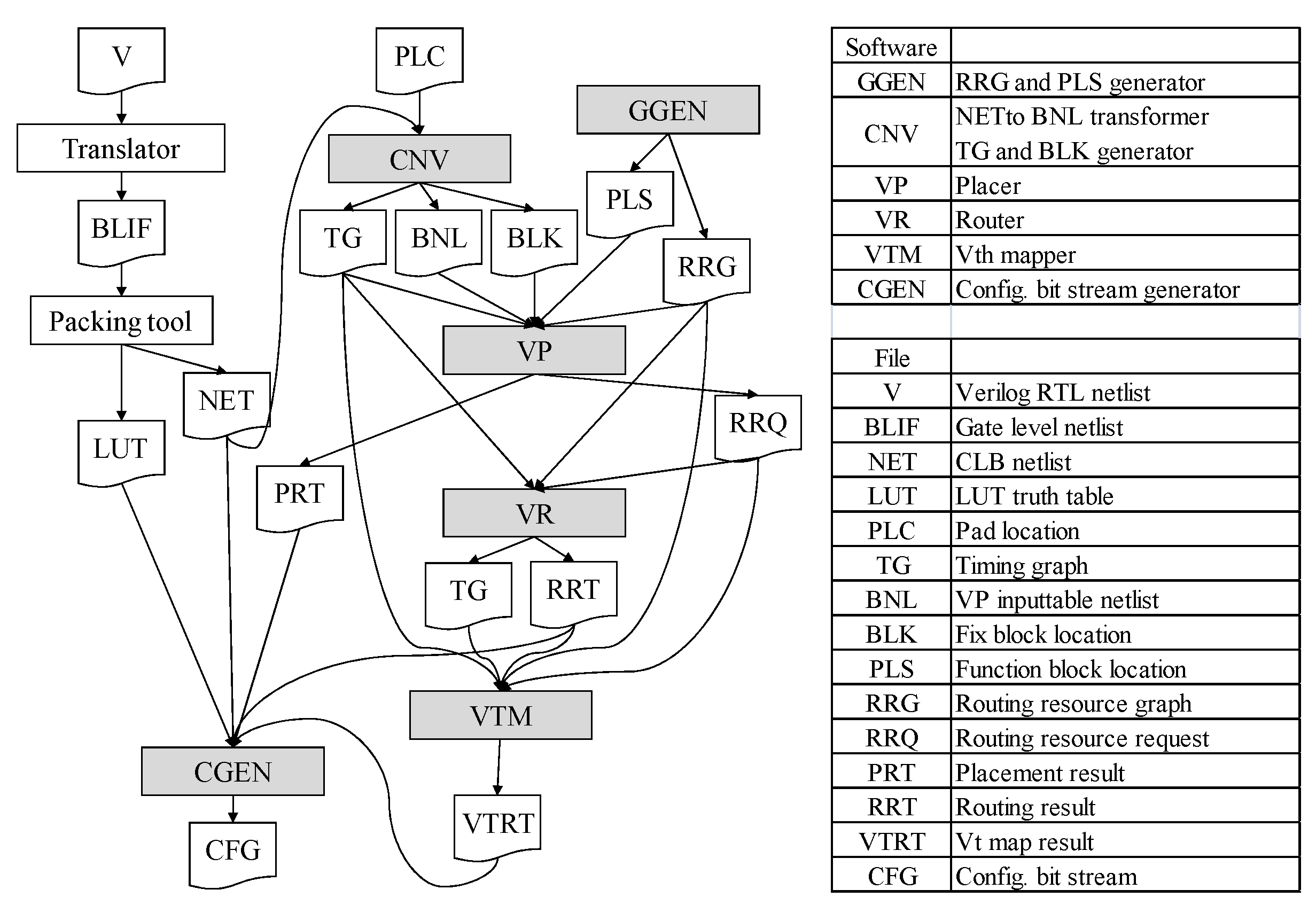
As shown in Figure 8, the dedicated CAD toolchain for Flex Power FPGA [9,11] includes newly introduced software, called Vt mapper (VTM), in addition to the conventional FPGA tools, such as placer and router. GGEN generates a routing resource graph that reflects the FPGA architecture. Then, logic synthesis and packing need to be performed beforehand for a target circuit. CNV translates and generates information for placement and routing phases. Next, placement and routing are subsequently performed by VP and VR, respectively. After that, VTM analyzes all signal paths and obtains the timing slack information in the user application design mapped on the Flex Power FPGA. Following this, timing slack is reduced on non-critical paths by slowing down the blocks in those paths. This is achieved by assigning the HVT state to as many Vt control domains as possible, while assigning the LVT state to the Vt control domains along the critical signal paths to keep the operation speed constant.
Figure 8. The dedicated CAD toolchain.
Jlpea 04 00188 g008
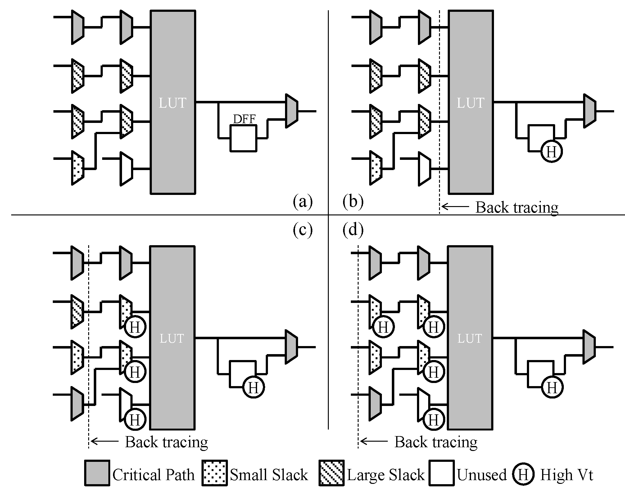
Figure 9 shows an example of the VTM behavior [9]. As shown in Figure 9a, the Vt of all nodes is set to LVT at the initial state. Then, the first step of the back tracing algorism in VTM is done, as shown in Figure 9b. The Vt of node on the critical path remains LVT, while unused DFF is set to HVT. Next, HVT is assigned to nodes having a large slack in Figure 9c. Finally, the VTM algorism is completed, as shown in Figure 9d.
Figure 9. Example of the Vt mapper (VTM) behavior [9] (a) initial state; (b) first step of the back trace; (c) HVT assignment; (d) VTM is completed.
Jlpea 04 00188 g009

3. Evaluation Results

3.1. Operating Speed and Static Leakage Current
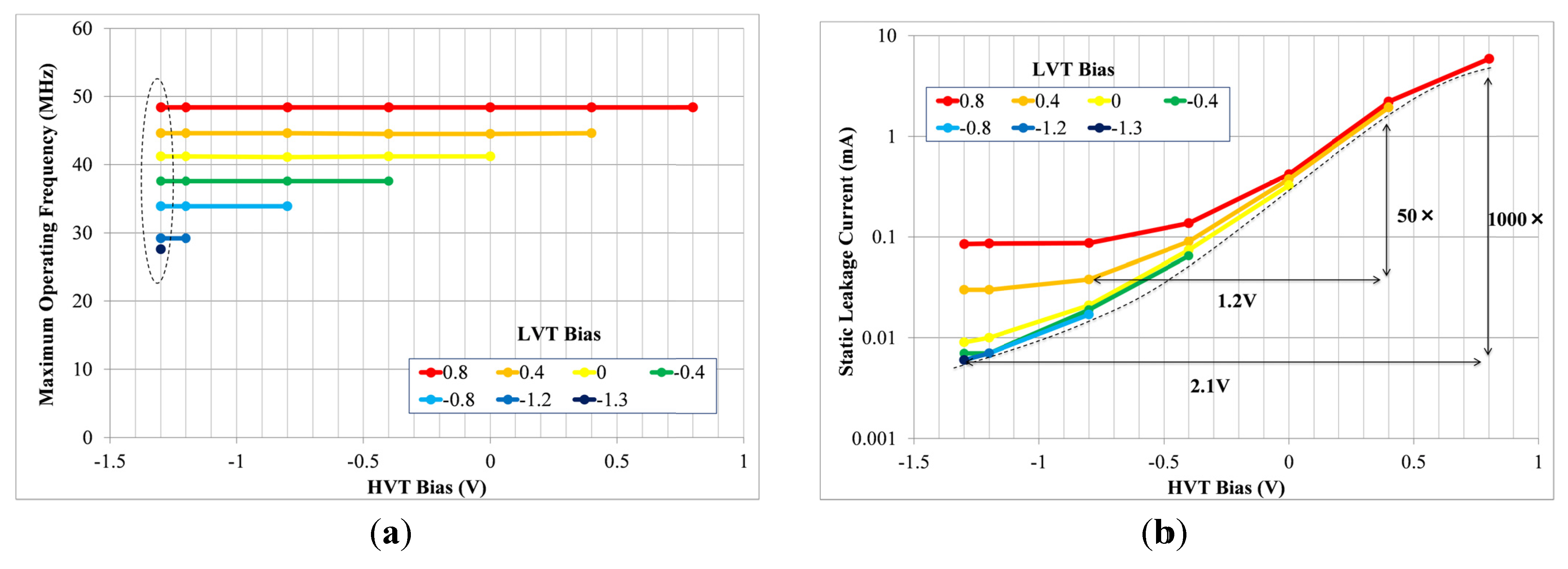
A 32-bit binary counter circuit is used as a sample application mapped onto the FPGA. The maximum operating frequency of the counter circuit and the static leakage current of the FPGA are measured in various bias voltage conditions. Bias voltages are chosen as follows: (1) the NMOS bias voltage for LVT (VBNL) is chosen from {−1.3, −1.2, −0.8, −0.4, 0.0, 0.4, 0.8}; (2) the NMOS bias voltage for HVT (VBNH) is chosen, so that VBNH ≤ VBNL; and (3) the PMOS bias voltages are appropriately determined from the corresponding NMOS bias voltages by subtracting from VDD. As a result, a total of 28 separate conditions are examined. The Vt mapper is re-executed condition by condition, so that the correct Vt mapping is produced based on the speed ratio of LVT and HVT.
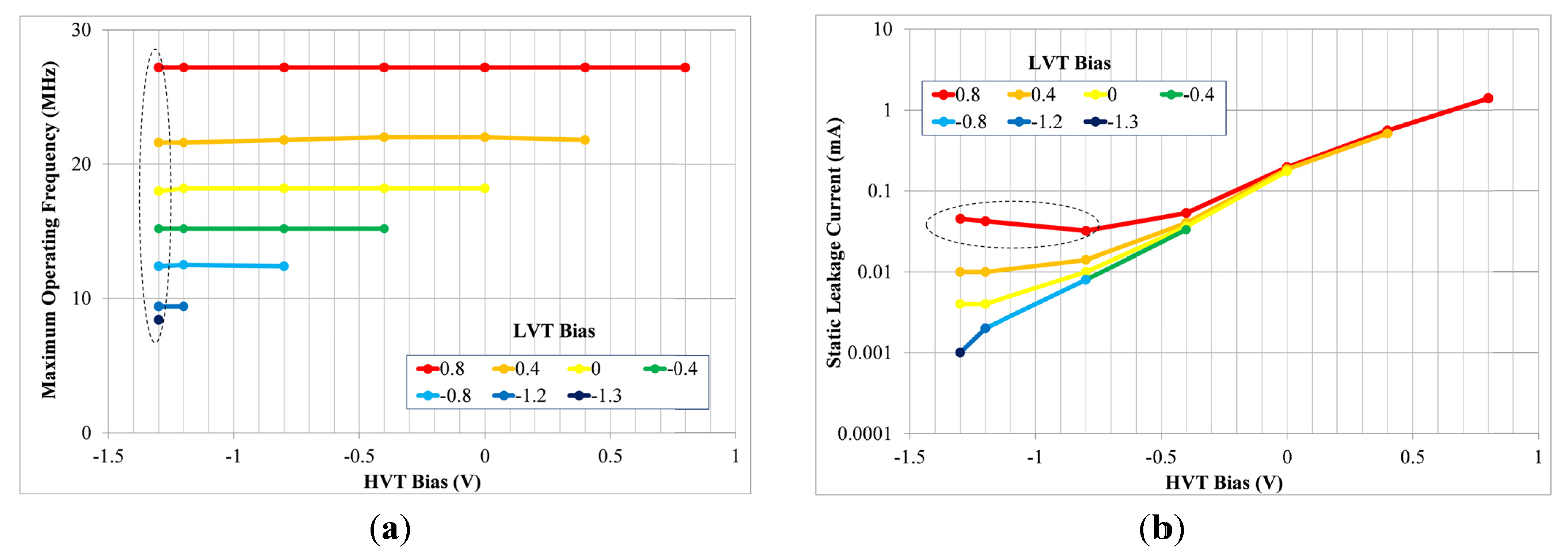
Figure 10a shows the measured maximum operating frequencies of the 32-bit binary counter circuit on various back-gate bias conditions. The core voltage of FPGA is set to 1.2 V. The horizontal axis shows the NMOS back-gate bias voltage for HVT (VBNH), and each line corresponds to the NMOS back-gate bias voltage for LVT (VBNL). The result shows that the operating speed can be widely controlled by the LVT bias voltage, which changes in the range from 0.8 V to −1.3 V when the HVT bias voltage is set to −1.3 V. Furthermore, the operating speed keeps a constant value against the change of the HVT bias voltages in the conditions of any LVT bias voltage.
Figure 10b shows the measured static leakage current on the various back-bias voltages. The supply voltage VDD is set to 1.2 V. Diagonal conditions or a contour line (dashed line) show the leakage characteristics of a single-Vt FPGA, where this means the condition in which the LVT bias is equal to the HVT bias. The single-Vt FPGA characteristic shows a three orders of magnitude static leakage reduction with a bias range of 2.1 V. This is a demonstration of the excellent Vt controllability of the SOTB transistor.
Figure 10. (a) Maximum operating frequency and (b) the static leakage measurement results in the various bias voltage conditions (VDD = 1.2 V).
Jlpea 04 00188 g010
With lowering of the HVT bias, each line for a specific LVT bias gradually departs from the contour line and is saturated. This is because the leakage current of HVT domains becomes negligibly small by lowering the HVT bias sufficiently, while the leakage current of LVT domains becomes dominant. When the HVT bias is relatively high, the leakage current of HVT domains, which accounts for a large percentage in the chip, is dominant. By comparing two points, for example, a 1.2-V bias difference achieves more than a 50× leakage reduction without degrading speed. A huge improvement of the static leakage reduction over 10× to 20× with bulk version [11] is obtained.
Figure 11 shows the maximum operating frequency and static leakage measurement results in the various bias voltage conditions. The core voltage of FPGA is lowered to 0.8 V to evaluate the behavior of the chip characteristics. As a result of the maximum operating frequency, the speed variation range becomes almost four times wider compared with Figure 8, in which VDD is set to 1.2 V. Another interesting point is that the static leakage current increases again after saturation, as indicated by the portion surrounded by a dashed line in the right figure. This is because the LVT is assigned to domains to be assigned originally as HVT, as discussed in [13]. First, the timing slack information in each building block is obtained after carrying out static timing analysis by the router included in the dedicated CAD toolchain, in the case that LVT is assigned to all building blocks. After that, in order, from the sink nodes, Vt mapper assigns HVT to the build blocks, satisfying that the timing slack is larger than the propagation delay difference between building blocks assigned as LVT and HVT. The Vt mapping process proceeds with decreasing the timing slack and is finally completed at the condition that the timing slack becomes smaller than the above-mentioned propagation delay difference. When the core voltage of the FPGA is set to 1.2 V, HVT is assigned to all building blocks on non-critical paths. However, when the supply voltage VDD is set to 0.8 V, LVT building blocks remain, because the timing slack is exhausted before assigning HVT to all building blocks on non-critical paths.
Figure 11. (a) Maximum operating frequency and (b) static leakage measurement results in the various bias voltage conditions (VDD = 0.8 V).
Jlpea 04 00188 g011

3.2. Overhead

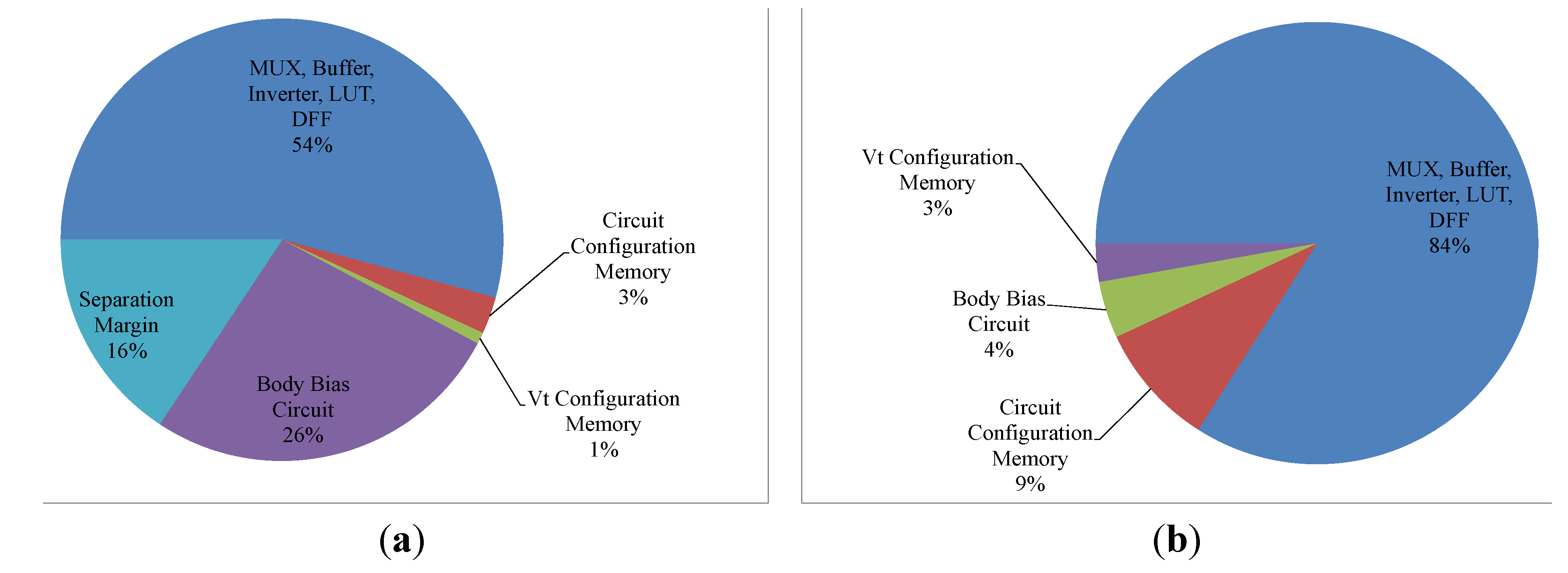
In order to program the Vt of elemental circuit components in an FPGA with a fine granularity, additional circuits, such as a body bias circuit, a bias voltage selector and configuration memory to store the Vt state information, and an extra separation margin between elemental circuits are needed. Figure 12a shows the area breakdown in the FPGA tile. The elemental circuits in FPGA, such as the MUX, buffer, inverter, LUT and DFF, occupy 54% of an FPGA tile area. The area of the configuration memory is only 3%. The Vt configuration memory, body bias circuit and separation margin occupies 1%, 26% and 16% of an FPGA tile area, respectively. An area overhead to control the Vt of an elemental circuit with a fine granularity becomes 43% of an FPGA tile area. The grain resolution for the Vt control is necessary to examine, because it directly affects the FPGA tile area. Figure 12b shows the breakdown of the static leakage current. The elemental circuits are applied to a zero body bias, resulting in the threshold voltage of the built-in state. The elemental circuits and configuration memory consume 93% of the static leakage current in an FPGA tile. On the other hand, the extra leakage current caused by the Vt configuration memory and body bias circuit is only 7%. This is because the body bias circuit is always applied to the reverse body bias, resulting in the higher Vt state, while the bias voltage selector is designed by a high-voltage transistor.
Figure 12. The breakdown of (a) the area and (b) the static leakage current in an FPGA tile.
Jlpea 04 00188 g012

4. Conclusions

The field programmable gate array (FPGA) is a promising target for advanced semiconductor technologies. However, static leakage is a serious problem in FPGAs. We have proposed an FPGA with fine-grained programmable body biasing, called the Flex Power FPGA, for static leakage power reduction. For further static power reduction, an excellent Vt controllability of the SOTB transistors can help a lot. The SOTB implementation of the Flex Power FPGA test chip is reported in this paper. The maximum operating frequency measurement results show that the operating speed can be widely controlled by the LVT bias, while the operating speed remains constant against the change in the HVT bias. Moreover, in the static leakage current measurement, the three orders of magnitude static leakage reduction with a bias range of 2.1 V demonstrates the excellent Vt controllability of the SOTB transistors. A 1.2 V bias difference achieves a 50× leakage reduction without degrading speed. The huge improvement of the static leakage reduction over 10× to 20× with the bulk version is obtained. The effectiveness of the Flex Power FPGA and the excellent Vt controllability of the SOTB transistor are clearly shown. The Flex Power FPGA is an important application target for this novel device.

Acknowledgments

This work was performed in the “Ultra-Low Voltage Device Project” of the Low-power Electronics Association and Project (LEAP) funded and supported by the Ministry of Economy, Trade and Industry (METI) and the New Energy and Industrial Technology Development Organization (NEDO).

Author Contributions

Masakazu Hioki designed the Flex Power FPGA architecture. Chao Ma measured the fabricated chips. Takashi Kawanami, Yasuhiro Ogasahara, Tadashi Nakagawa, Toshihiro Sekigawa and Toshiyuki Tsutsumi discussed the results of this paper. Hanpei Koike coordinated this research project.

Conflicts of Interest

The authors declare no conflict of interest.

References

  1. Kuon, I.; Rose, J. Measuring the Gap between FPGAs and ASICs. In Proceedings of the 2006 ACM/SIGDA 14th International Symposium on Field Programmable Gate Arrays, Monterey, CA, USA, 22–24 February 2006; pp. 21–30.
  2. Li, F.; Lin, Y.; He, L.; Cong, J. Low-Power FPGA Using Predefined Dual-Vdd/Dual-Vt Fabrics. In Proceedings of the 2004 ACM/SIGDA 12th International Symposium on Field Programmable Gate Arrays, Monterey, CA, USA, 22–24 February 2004; pp. 42–50.
  3. Rahman, A.; Polavarapuv, V. Evaluation of Low-Leakage Design Techniques for Field Programmable Gate Arrays. In Proceedings of the 2004 ACM/SIGDA 12th International Symposium on Field Programmable Gate Arrays, Monterey, CA, USA, 22–24 February 2004; pp. 23–30.
  4. Gayasen, A.; Tasi, Y.; Vijaykrishnan, N.; Kandemir, M.; Irwin, M.J.; Tuan, T. Reduced Leakage Energy in FPGAs Using Region-Constrained Placement. In Proceedings of the 2004 ACM/SIGDA 12th International Symposium on Field Programmable Gate Arrays, Monterey, CA, USA, 22–24 February 2004; pp. 51–58.
  5. Anderson, J.H.; Najim, F.N. Low-Power Programmable Routing Circuitry for FPGAs. In Proceedings of the 2004 IEEE/ACM International Conference on Computer-aided Design, Washington, DC, USA, 7–11 November 2004; pp. 602–609.
  6. Lin, Y.; Li, F.; He, L. Routing Track Duplication with Fine-Grained Power-Gating for FPGA Interconnect Power Reduction. In Proceedings of the 2005 Asia and South Pacific Design Automation Conference, Shanghai, China, 18–21 January 2005; pp. 645–650.
  7. Rahman, A.; Das, S.; Tuan, T.; Rahut, A. Heterogeneous Routing Architecture for Low-Power FPGA Fabric. In Proceedings of the IEEE Custom Integrated Circuits Conference 2005, San Jose, CA, USA, 21 September 2005; pp. 183–186.
  8. Tuan, T.; Kao, S.; Rahman, A.; Das, S.; Trimberger, S. A 90 nm Lowpower FPGA for Battery-Powered Applications. In Proceedings of the 2006 ACM/SIGDA 14th International Symposium on Field Programmable Gate Arrays, Monterey, CA, USA, 22–24 February 2006; pp. 3–11.
  9. Kawanami, T.; Hioki, M.; Nagase, H.; Tsutsumi, T.; Nakagawa, T.; Sekigawa, T.; Koike, H. Preliminary evaluation of flex power FPGA: A power reconfigurable architecture with fine granularity. IEICE Trans. Inf. Syst. 2004, 8, 2004–2010. [Google Scholar]
  10. Tsuchiya, R.; Horiuchi, M.; Kimura, S.; Yamaoka, M.; Kawahara, T.; Maegawa, S.; Ipposhi, T.; Ohji, Y.; Matsuoka, H. Silicon on Thin BOX: A New Paradigm of the CMOSFET for Low-Power High-Performance Application Featuring Wide-Range Back-Bias Control. In Proceedings of the IEEE International Electron Devices Meeting 2004, San Francisco, CA, USA, 13–15 December 2004; pp. 631–634.
  11. Hioki, M.; Sekigawa, T.; Nakagawa, T.; Kawanami, T.; Matsumoto, Y; Tsutsumi, T.; Koike, H. Fully-Functional FPGA prototype with Fine-Grain Programmable Body Biasing. In Proceedings of the ACM/SIGDA International Symposium on Field Programmable Gate Arrays, Monterey, CA, USA, 11–13 February 2013; pp. 73–80.
  12. Sugii, N.; Tsuchiya, R.; Ishigaki, T.; Morita, Y.; Yoshimoto, H.; Kimura, S. Local Vth Variability and Scalability in Silicon-on-Thin-Box (SOTB) CMOS with Small Random-Dopant Fluctuation. IEEE Trans. Electron Devices 2010, 57, 835–845. [Google Scholar] [CrossRef]
  13. Kawanami, T.; Hioki, M.; Matsumoto, Y.; Tsutsumi, T.; Nakagawa, T.; Sekigawa, T.; Koike, H. Optimal Set of Body Bias Voltages for an FPGA with Field-Programmable Vth Components. In Proceedings of the 2006 IEEE International Conference on Field Programmable Technology, Bangkok, Thailand, 13–15 December 2006; pp. 329–332.