1. Introduction
Linear Feedback Shift Registers (LFSRs) are widely utilized in various electronic systems requiring the generation of pseudorandom binary sequences (PRBS). Common applications include built-in self-test (BIST) of digital circuits [
1,
2,
3,
4,
5,
6,
7,
8,
9,
10,
11], where minimizing power, delay, and area is critical. Additionally, LFSRs serve as core components in stream ciphers for secure communications [
12,
13,
14,
15,
16].
BIST is a Design-for-Testability (DFT) technique that embeds test logic within the chip to autonomously identify faults. It has emerged as a practical solution to VLSI testing challenges due to its advantages, such as (a) enabling at-speed and in-field testing, (b) improved testability, (c) reduced dependence on automatic test equipment (ATE), (d) enhanced flexibility and customization, and (e) support for periodic and online testing. Among various pattern generators used in BIST, LFSRs are especially favored because of their low area overhead, efficient fault coverage, scalability, and inherent randomness.
While the pseudorandom nature of LFSR-generated patterns benefits certain applications like cryptography, the low correlation between consecutive patterns results in high switching activity during test applications. This leads to increased dynamic power consumption. In scan-based testing, the impact is even more severe due to higher switching in scan chains, raising the risk of thermal stress or even permanent damage to the Circuit Under Test (CUT). Factors such as concurrent activation of internal cores and power-hungry DFT circuits further exacerbate this issue [
17,
18,
19,
20,
21,
22]. Thus, controlling test power is a major design consideration during LBIST implementation.
A wide range of approaches have been explored to reduce test power [
11,
21,
23,
24,
25,
26,
27,
28,
29,
30,
31,
32,
33]. These include techniques like (i) test scheduling algorithms, (ii) low-power RAM testing, (iii) toggle suppression, (iv) LFSR tuning, (v) vector filtering BIST, (vi) circuit partitioning, and (vii) low-power test pattern generators. Among these, modifying the test pattern generator stands out due to its direct influence on power and ease of integration within existing BIST frameworks.
This paper proposes a novel low-power test pattern generator that is based on a tiered or bipartite LFSR architecture. To reduce the transition density in generated vectors, the design incorporates a zero-forcing logic. The aim is to improve correlation between test patterns, thereby lowering scan-in power.
In [
34], Dual-LFSR (DL) and Quad-LFSR (QL) architectures were proposed for BRLWE-based cryptographic schemes. These parallelized hardware designs achieved 1.6× and 2.7× reductions in computational time, respectively.
Learning with Errors (LWEs) is a foundational cryptographic problem involving the solution of linear equations perturbed by small errors. Proposed by Regev in 2005, LWEs is computationally difficult due to matrix–vector operations. Its ring variant, Ring Learning with Errors (RLWEs), improves efficiency by operating in a polynomial ring, reducing key size. Binary Ring Learning with Errors (BRLWEs) further simplifies implementation by replacing Gaussian-distributed errors with binary errors, making it attractive for hardware realization. Nevertheless, the area-delay product (ADP) in BRLWE-based architectures still requires optimization.
To meet performance, area, and power targets, LFSR design strategies now emphasize advanced topological structures, high fault coverage under low-power constraints, and parallelism. Implementing LFSRs on FPGAs provides design flexibility and rapid prototyping across various polynomial degrees and feedback taps. Moreover, FPGA-based implementations support reconfigurability, making them suitable for dynamic verification and reduced time to market.
Despite their strong statistical properties, LFSRs generate output patterns that follow linear recurrences. The fixed feedback taps define the recurrence relation, which can be mathematically predicted, thus limiting the suitability of LFSRs for cryptographic functions [
35].
In the context of LBIST, the pseudo-random patterns with low inter-pattern correlation exacerbate power consumption during scan shifting. This phenomenon, known as scan-in power, can be mitigated by reducing toggle rates through modifications in the Test Pattern Generator (TPG). For example, the programmable LFSR in [
30] incorporates a two-stage design to reduce transition density, thus lowering dynamic power consumption.
Several studies have investigated the design of LFSR-based pseudorandom pattern generators. While some aim to maximize pattern diversity, they often do so at the cost of higher power or area. Others fail to provide sufficient flexibility or reconfigurability. This work presents an architecture that combines multiple LFSRs operating over a polynomial ring of the form
where
p is the degree of the polynomial. The goal is to enhance pattern diversity, reduce power consumption, and ensure hardware efficiency through structural innovations. The major contributions of this work are
A method to increase the correlation between generated patterns by segmenting the polynomial and combining with zero forcing, which significantly contributes towards power reduction.
Creating distinct sets of pseudorandom patterns by programming the coefficients in feedback along with the initial seed values or configurability based on the user requirements.
The rest of this paper is organized as follows:
Section 2 presents the background and related work, while
Section 3 discusses the proposed design.
Section 4 showcases the simulation results and analysis.
Section 5 provides a comparison of the results, and finally,
Section 6 concludes the paper with a summary and future scope.
2. Preliminaries
Pseudo-random binary sequence (PRBS) generators are registers with input bits from a function of a prior output state. The outputs are a set of pseudorandom sequences based on an initial value known as a seed. The function of LFSR is generated by connecting the XOR function at tap points, which is decided by a characteristic polynomial. Thus, an
m-bit LFSR traditionally spans using controlled D-type storage elements (DFFs) and an interconnected system of feedback routes regulated by coefficient switches represented as
. The D-Flip flop outputs are routed to XOR gates, as demonstrated in [
34,
35,
36]. The quantity of D-Flip flop signifies the degree (
m) of an LFSR, which regulates the number of patterns in the output sequence. The longest possible duration (period,
L) is assigned by
Based on the circuit structure, two fundamental circuit classifications evolved: Galois (Internal or Type 1 or Modular) feedback and Fibonacci (External or Type 2 or Standard) feedback LFSR, which are duals and are given in
Figure 1 and
Figure 2 respectively. Comparisons between the two structures reveal that Galois provides the leading frequency of operation required for high-performance applications, while Fibonacci offers the advantage of uniformity of the shift register [
37,
38].
Depending on whether the characteristic polynomial is primitive or non-primitive, both Galois or Fibonacci can generate
or a lesser number of sequences, which can be updated using extra circuitry to create all
sequences where
m is the degree of the polynomial. An initial seed value is required to start the sequence generation and the process of preloading these values is known as
reseeding the LFSR. The seed loading process is made viable through integrating multiplexer modules into the circuit. The structure of an LFSR with degree
m, on the other hand, may be anticipated by the feedback coefficients
and the output states’ patterns because of its deterministic period, which is outlined by the following Equation (
3) [
35]:
Consider that the LFSR is primarily loaded with values
,
, …
, then the next output bit
which forms the input to the leftmost D-FF of the LFSR, can be processed by the sum-XOR of D-FFs outputs and subsequent feedback coefficients
; thus, developing Equation (
3):
Thus, Equation (
4) identifies
m linear sets of equations involving sequences, with constant
values throughout all equations. If the coefficients
s diverge with newfound states, then Equation (
4) becomes void and cannot be credibly used for estimating the coefficients
s.
2.1. Evaluation of Periodicity and Randomness
LFSRs have solid statistical attributes when the coefficients are selected effectively to achieve a possible largest length. Furthermore, for an assumed degree
m, an LFSR can generate patterns of varying durations (periods) decided by the feedback coefficients as well as the starting state of the LFSR. The polynomial given in Equation (
5) represents an LFSR with a feedback coefficient vector (
,
,
,……
) [
35].
To give an example, the coefficient (
) represents the primitive polynomial,
. Thus, primitive polynomials can vary based on feedback coefficients and initial charging states. Proper coefficients and launching state choices allow for the deployment of maximum-length sequences with high linear complexity. The linear complexity profile measures how “random” or “structured” a sequence is. Primitive polynomials are specific forms of irreducible polynomials that are approximately equivalent to prime numbers in that they have only one factor: the polynomial itself. Primitive polynomials may be computed rather readily and consequently, maximum-length LFSRs are trivial to identify. For each given degree
m, several primitive polynomials can be evolved and generally, there are many possible primitive polynomials for every given degree
m. As an example, the literature [
39] states that there are 69,273,666 distinct primitive polynomials for degree
m = 31. Linear complexity is the primary characteristic for assessing the unpredictability of a key stream. The linear complexity test of LFSRs represented by a primitive polynomial of degree
m is L/2 because an LFSR primitive polynomial stimulates an L number of sequences within its period [
40]. The dynamic behavior of the linear complexity test for the first
n of generated patterns for Fibonacci with degree
m = 4 and polynomial
with the charging state [0010] is given in
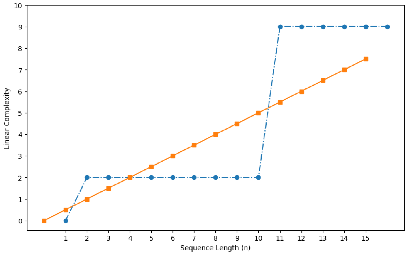
Figure 3. The blue coloured graph represents the profile for the Fibonacci LFSR and orange colored graph represents that for L ≈
n/2. This profile graph is near L/2 in its overall period, in which L(
) = 15. In essence, if L ≈
n/2, the sequence has high linear complexity, and if L ≪
n/2, the sequence has low linear complexity. Consequently, the linear complexity profile for LFSR circuits with primitive polynomials that change according to feedback coefficients and starting charge states is deemed suitable and decent for the representation of statistical pseudo-randomness.
2.2. Understanding Power Reduction
Compared to static power resulting from leakage currents, dynamic power is the primary source of power consumption in LFSR and is proportional to the circuit’s switching activity. Equation (
6) represents the dynamic power of the circuit. Mitigation of dynamic power can be achieved by techniques such as (a) reduced switching activity, (b) segmented LFSR, (c) gated clocking, and (d) low-transition designs.
where switching activity is represented by
, load capacitance is
, supply voltage is
, and clock frequency is given by
f. While lowering the supply voltage significantly decreases power usage, reliability and circuit speed may be impacted. The capacitance
is determined by the physical layout and technology utilized; therefore, reducing the value may necessitate adjustments to the design. Minimizing switching activity strategies such as (1) using low-transition LFSR designs or (2) clock gating and methods like segmentation and parallelism contribute to minimizing the activity component,
. The tradeoffs and considerations during the reduction of dynamic power are as follows: (a) Power vs. performance: reducing dynamic power frequently results in decreased performance (e.g., slower speed owing to lower frequency or voltage). Designers must strike a balance between power efficiency and performance requirements. (b) Complexity: using advanced approaches such as clock gating or dual-polynomial LFSRs might complicate the design, necessitating more sophisticated control logic and verification processes. The segmentation and parallelism method in low-power LFSR design consists of strategies to divide the LFSR into smaller segments that function independently, thereby allowing each segment to be clocked less frequently, lowering the total switching activity and dynamic power. This work investigates slicing a specific LFSR into two to reduce complexity and, consequently, hardware overhead. Because of its segmented architecture, the proposed approach can consume less power while ensuring consistency across all configurations and bit lengths.
3. Proposed Circuit
The objective is to use two consecutive low-correlated sequences to generate a highly correlated sequence, which involves injecting a new test vector between them with a significantly reduced hamming distance. Consequently, these patterns have a shorter hamming distance, which decreases the rate of toggling and, thus, the dynamic power of the circuit.
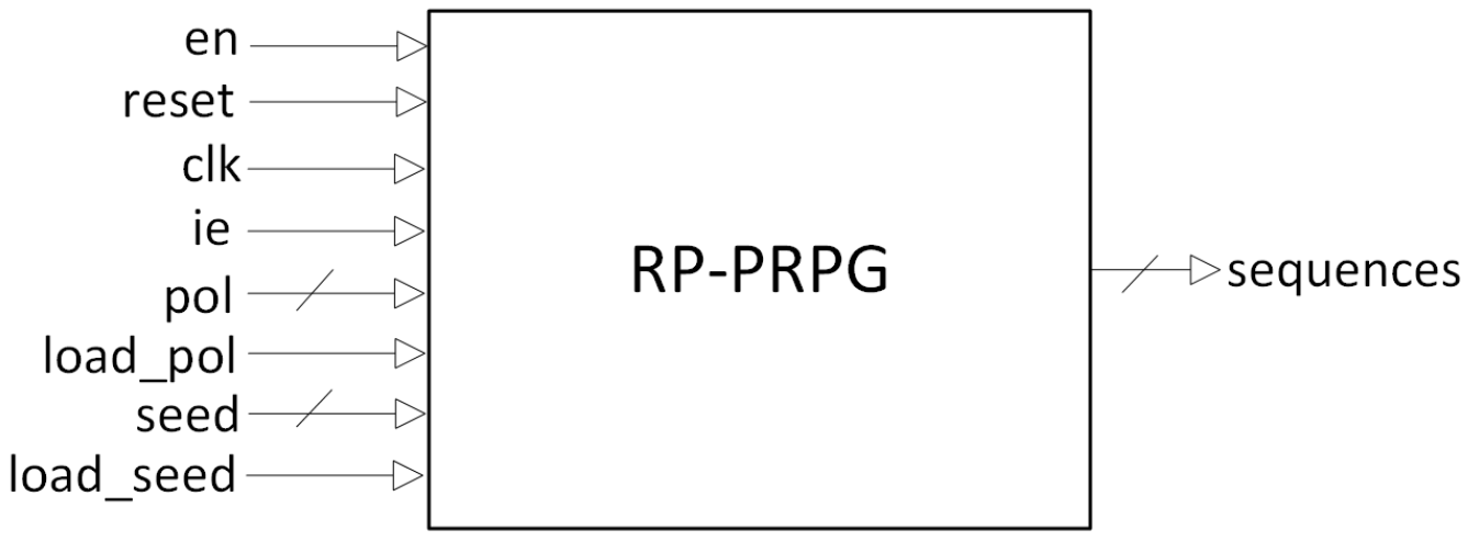
Figure 4 illustrates the top-level description for the proposed RP-PRPG with input
seed for the initial seed value and the
input, which is used to charge these values through the application of a high value. The value at
ie decides whether the circuit works as a Fibonacci or Galois circuit. The input
pol chooses the set of coefficients to be tailored according to the configuration determined using
ie, and the entire operation is wrapped up using a high value in
. The clk signal acts as the dominant clock for the design which can be employed to regulate other sequential segments in the circuit. When enabled, the
reset signal resets all of the output values and the
en pin operates to activate the circuit. Outputs with reduced hamming distance are deployed using the
sequences out pin.
Figure 5 illustrates the envisioned overall circuit architecture of the RP-PRPG using Fibonacci adopted for the convenience of description; higher degrees have identical constitutions but are more expansive in dimensions. The primary components of the proposed technique are a two-segment LFSR and a zero-forcing circuit. Clk1, Clk2, and Clk3 are split in the ratio 1:2:1, ensuring that no clocks operate simultaneously. The LFSR’s partitioning is based on the MSB and LSB bits, and it is controlled by two clocks generated from the main clock. These derived clocks determine whether the first or second segment is operational at any given moment. Since only one segment is active at a given time, an extra flip-flop is required to maintain the data flow between both segments, even if it propels the area overhead. A zero-forcing circuit places zero between bits that have a difference in state value. Typically, the patterns generated are pseudorandom, with minimal pattern correlations, resulting in a higher hamming distance. Using this method, the transition between subsequent bits is significantly reduced. A larger hamming distance immediately increases power consumption during testing, which we mitigate in our design by segmenting the LFSR based on bit size.
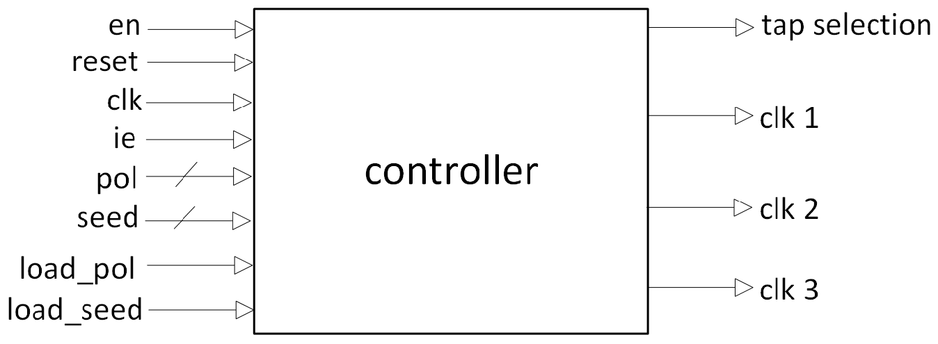
Figure 6 shows the functioning of the controller that generates control signals for the circuitry. This brings in three clock signals for the RP-PRPG as well as the tap selection. The derived clock signals dictate which segment in the RP-PRPG produces the sequences. A high value in the clock signal enables a segment, which thus generates sequences while other segment stays idle. Any of the three derived clocks can be enabled within a single cycle of the primary clock. Two of the clocks correlate to the two segments and the connection flip-flops, while the third clock relates to the zero forcing circuit.
Two-segment LFSR is a setup that involves dual segments of LFSR with a connector flip-flop. The data is separated into two layers: MSB in the first tier and LSB in the second tier, with the flip-flop serving as a link between the two. The data is subsequently sent via a zero-forcing circuit, which aids to decrease the quantity of transitions between two output patterns. If any of the bits in two consecutive patterns change, they are forced to zero.
Table 1 depicts the process of reduction in transition, with a new sequence introduced between two successive sequences: seq1 and seq1. The entire number of transitions between seq1 and seq2 is divided across the new sequence s’. The total number of transitions between seq1-s’ and s’-seq2 will be the same as for the conventional sequence seq1-seq2.
The clock determines whether the output is from the dual-layer LFSR or the zero-forced output. The dual-tier LFSR sends the test vector to the zero forcing circuit, where the previous and current test vectors are compared and the new vector is sent out as the next test vector, since the transitions will be fewer in number. Thus, zero forcing adds a new vector between all test vector pairs from the LFSR.
4. Simulation & Performance
The RP-PRPG described in
Figure 5, is built and evaluated in HDL Verilog, thus enabling quick reconfiguration and functional verification for the different bit lengths and circuit configurations. ModelSim was used for functional verification, while Xilinx VivadoSuite 2015 was used for implementation on the Artix-7 FPGA board, which was developed using 28nm high-performance, low-power (HPL) technology. This provides an excellent blend of power, efficiency and performance, making them suitable for applications including communication, automotive, and industrial equipment. This section presents the results of the circuit simulation across various bit combinations, configurations and output patterns.
Figure 7 and
Figure 8 illustrates and compares the simulation wave patterns for 8-bit versions of conventional Fibonacci LFSR and the proposed design built on the primitive polynomial
, whereas
Figure 9 and
Figure 10 shows a similar comparison for Galois LFSR configuration of the same polynomial. The violet color in the waveform shows the pattern’s transition count, while the cyan color represents the seed values utilized and the polynomial. All these circuits utilized a seed value of
across all configurations and all these circuits generate all 256 patterns and are evaluated for several output patterns, as shown in
Table 2. All the circuits are compared for 100 to 500 number of output sequences. Columns three and six correspond to the transition count of the Fibonacci and Galois configuration of the proposed design and comparing these values against the transition count of conventional circuits, it can be verified that the number of transitions is lower for the proposed circuit. The percentage reduction of transitions for both cases is given in columns four and seven and in all cases the percentage reduction is greater than 70%.
The LFSR polynomial is parameterized in HDL code, since it is typically used only once before an operation, decreasing the number of primary pins required. The design was modeled for 4-, 8-, 16-, 32-, 64-, and 128-bit LFSRs with primitive polynomials, and the same number of output patterns, comparing the number of transitions between the proposed and conventional LFSR structures. For both conventional and proposed LFSR, the transition counter keeps track of the number of transitions that occur in their output.
Table 3 and
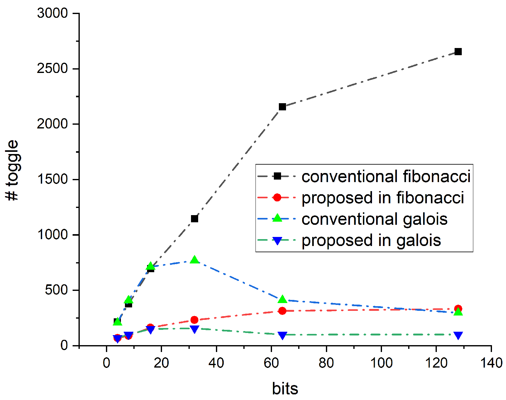
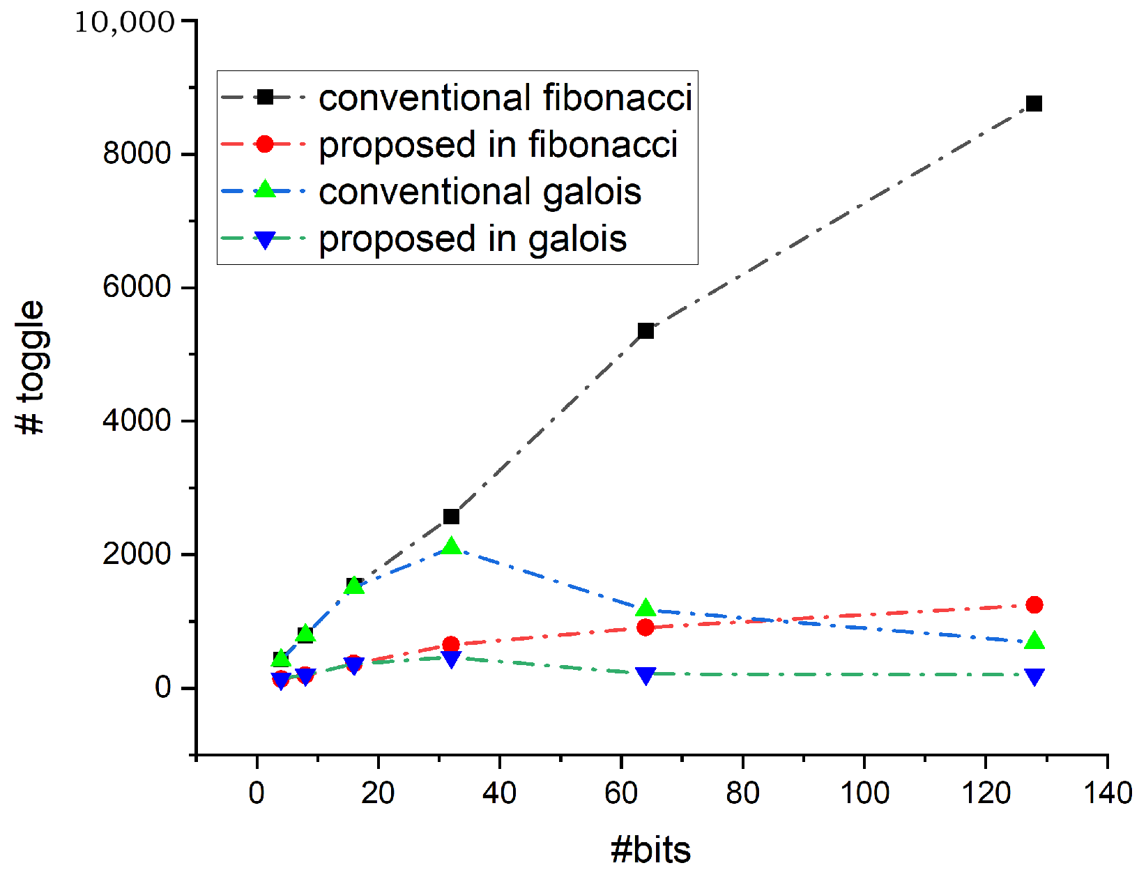
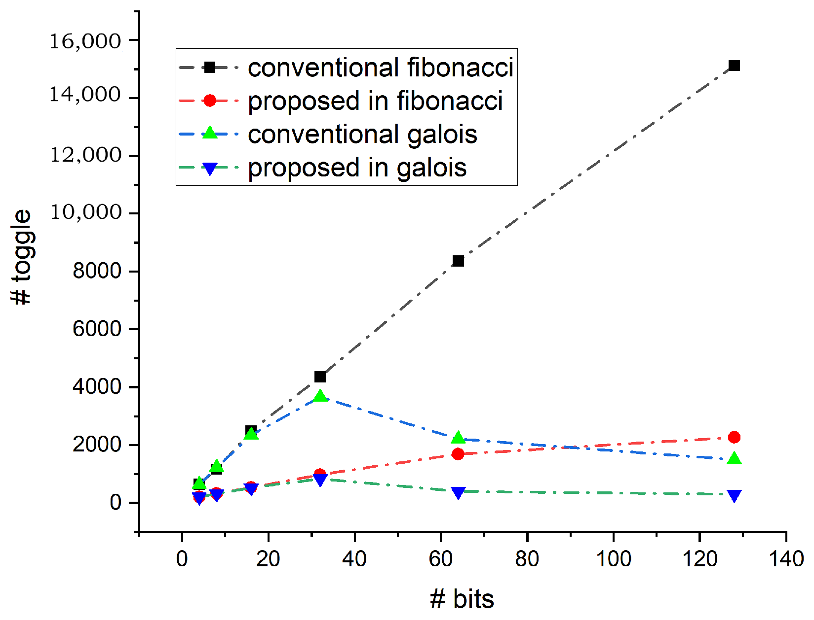
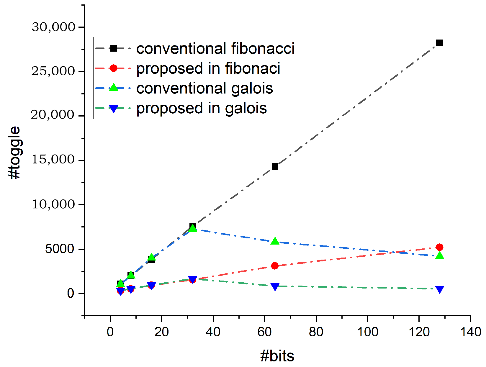
Table 4 illustrate the simulation insights across different parameters, configurations, and output patterns. To examine and analyze the decrease in transition count between 4, 8, 16, 32, 64, and 128-bits in the proposed design and the classic LFSR, both designs were simulated for the same polynomials and for 100, 200, and 500 output patterns. The toggle reduction in both Fibonacci and Galois configurations is analyzed for an equal number of output sequences.
Figure 11 shows the number of toggles obtained for both these configurations for 100 output patterns. The toggles are reduced in the proposed design in both the Fibonacci as well as the Galois configuration. Similarly,
Figure 12,
Figure 13,
Figure 14 and
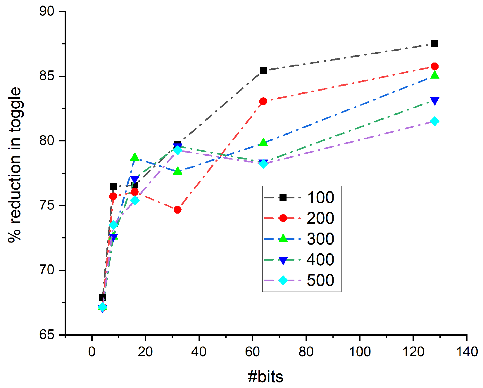
Figure 15 represents the reduction in the toggle for 200, 300, 400, and 500 output patterns in both configurations. The percentage reduction in the toggle is plotted for the Fibonacci configuration and is given in
Figure 16. It shows that the reduction percentage increases consistently once the number of bits crosses 60. Depending on the polynomial under consideration, this value can change. Thus, after this value, the toggle rate shows a reduction of more than 80%. Similarly, the percentage reduction of the toggle rate is calculated for the Galois configuration and is given in
Figure 17. The percentage reduction in toggling is lower for 100 runs compared to 500 runs. As more patterns are considered, the toggle reduction percentage improves.
The proposed design is implemented in the Artix-7 FPGA board.
Table 5 shows the implementation results across different bits of the proposed design for 10 ns clock. The total on-chip power dissipation shows only a variation from 0.133W to 0.21W when the polynomial degree changes from 4 to 128, which is approximately 57.89% only. The flip-flop count increases from 14 to 388, and the LUT usage rises from 37 to 728 from 4 to 128 bits. Despite this, the power overhead is limited to just 57.89%, indicating that the increase in resource usage has minimal impact on overall power consumption. The results are compared against a baseline conventional architecture (given in
Table 6) that does not incorporate any low-power techniques, as in the proposed design.
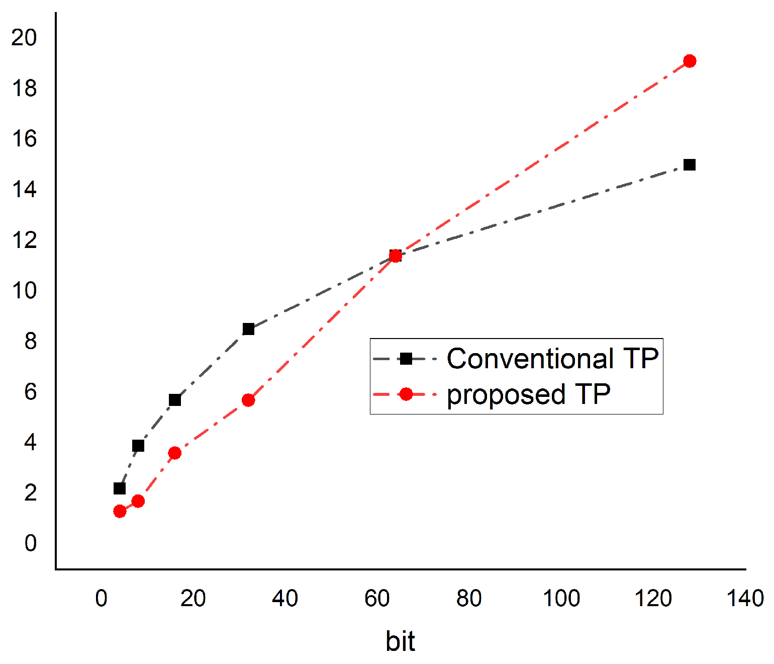
Table 7 provides a detailed comparison between the proposed and conventional LFSR-based pattern generators across various bit-widths. The proposed architecture demonstrates a consistent enhancement in throughput, particularly at higher bit-widths, achieving 19.1 bits/cycle at 128 bits compared to 15 bits/cycle in the conventional counterpart. While there is a moderate increase in power-delay product (PDP), this trade-off is offset by the improved data delivery rate and operating frequency. The area-delay product (ADP) is higher for the proposed design due to additional control logic required for transition minimization. Nonetheless, the design exhibits favorable scalability and energy efficiency, indicating its suitability for low-power BIST applications where high-speed test pattern delivery is critical.
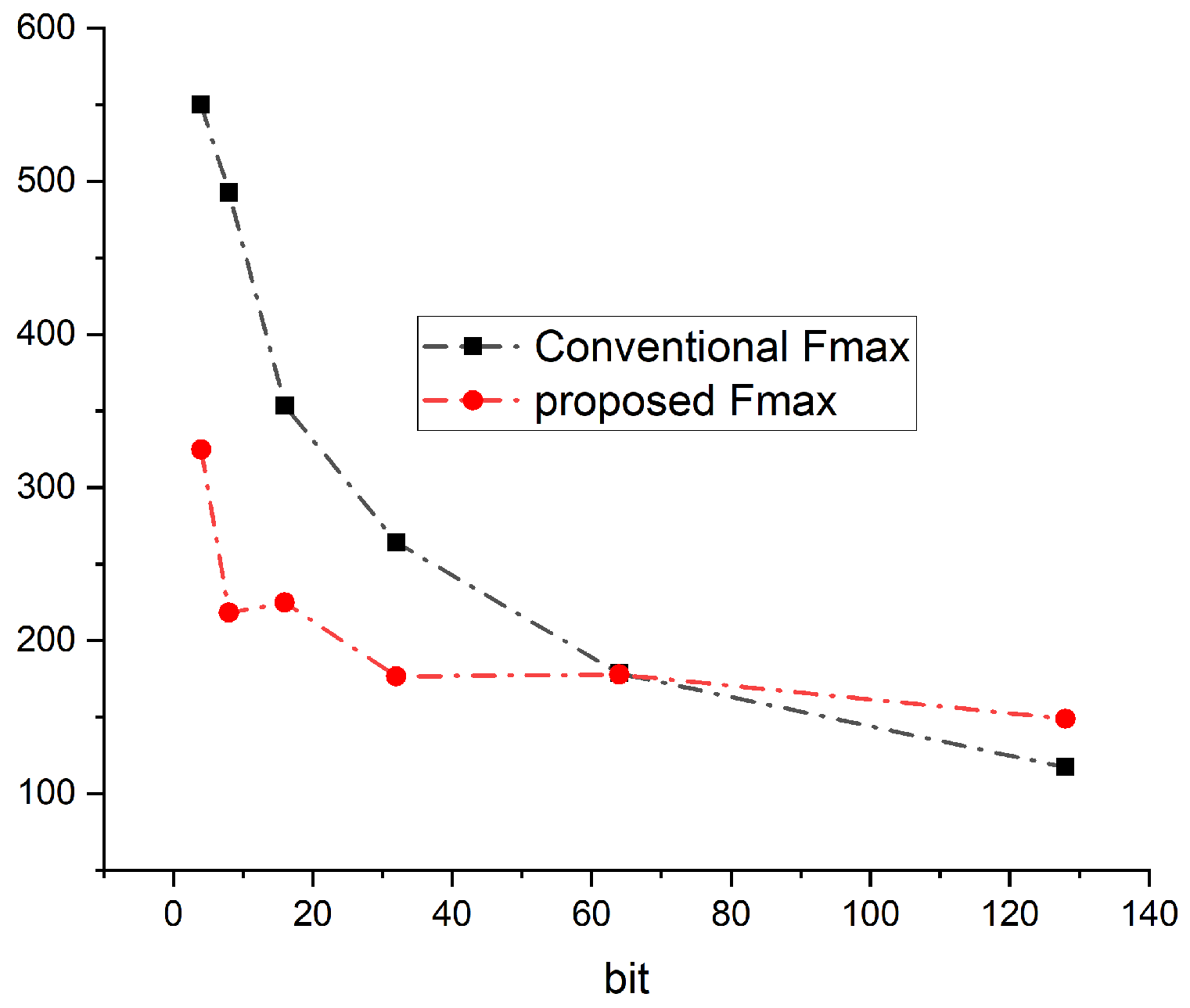
As the bit-width increases (particularly at 64 and 128 bits), the proposed design achieves competitive or in some cases superior maximum operating frequency compared to the conventional structure, demonstrating improved scalability, as illustrated in
Figure 18. Moreover, the proposed approach consistently delivers higher throughput across all configurations, highlighting its efficiency in pattern generation, as shown in
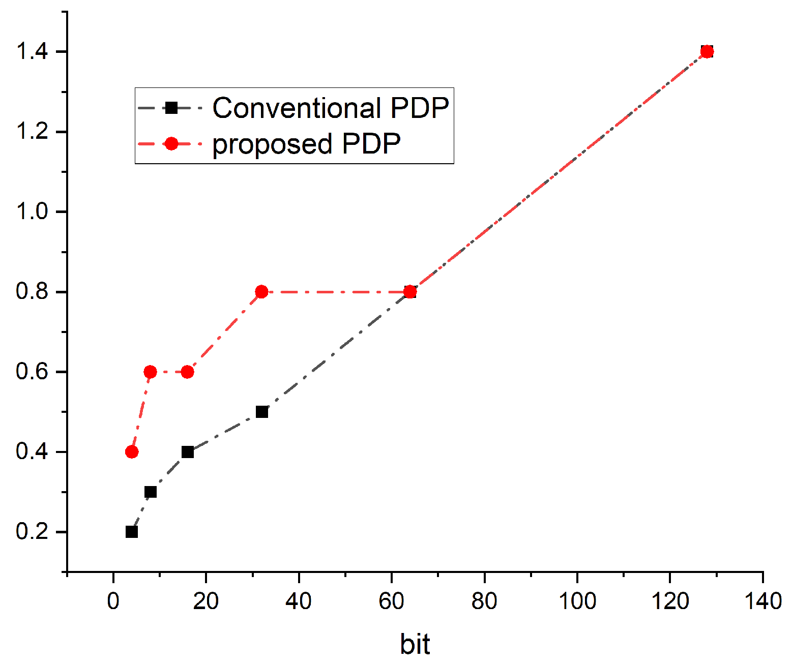
Figure 19. For instance, at 128 bits, the proposed design achieves a throughput of 19.1 compared to 15 in the conventional case, ensuring better data availability per clock cycle—an important factor for high-speed test applications. The Power Delay Product (PDP), which reflects energy efficiency (with lower values being preferable), is presented in
Figure 20. Although the proposed design exhibits a slightly higher PDP across all bit-widths—primarily due to the additional logic for transition control—the increase remains modest (e.g., 0.6 vs. 0.5) and is justified by the significant improvements in throughput and scalability.
Additional randomness tests, such as those from the National Institute of Standards and Technology (NIST) [
41], are conducted to evaluate randomization criteria, as shown in
Table 8. Statistical benchmark tests are run on 128 bit-length with 8000 sequences created by the RP-PRPG and compared to a conventional LFSR with the same configuration.
Table 7 shows that if a pseudorandom bit sequence’s
p-value surpasses the threshold in all tests, it is considered random. It covers the following tests: a random excursion test, frequency (monobit) test, approximate entropy test, non-overlapping template matching test, frequency test within a block, runs test, test for the longest run of several runs in a block, binary matrix rank test, overlapping template matching test, Maurer’s “Universal Statistical” test, linear complexity test, serial test, cumulative sums (Cusum) test, and random excursion variant test.
The gathered sequences with a size of 1,024,000 bits passed these tests. To summarize, the proposed RP-PRPG has generally better statistical features compared to conventional LFSR. The overlapping template-matching test, Maurer’s “Universal Statistical” test, and linear complexity test were successful and in other cases the p-values were higher than those observed for conventional LFSR. The overlapping template-matching test focuses on the number of occurrences of pre-specified target strings. Maurer’s “Universal Statistical” test aims to determine the number of bits between matching patterns (a measure related to the length of a compressed sequence). The test determines whether or not the sequence can be greatly compressed without losing information. A highly compressible sequence is deemed non-random. The linear complexity test focuses on the length of a linear feedback shift register (LFSR). The goal of this test is to see if the sequence is complicated enough to be deemed random. Random sequences have longer LFSRs. An LFSR that is too short indicates non-randomness. Pattern generators built for use in cryptographic applications may need to meet more stringent requirements than for different applications. In particular, their outputs must be unpredictable in the absence of knowledge regarding their inputs.
5. Comparison Investigation
Numerous researchers have explored low-power test pattern generation techniques, including gated clock techniques, adaptive power management, weighted random pattern generators, using control logic to decide the process of pattern generation based on power constraints, and the use of multiple polynomial, hybrid test patterns, pattern compression techniques, and low-transition methods. Our work focuses on reducing the power by managing the toggle count by adapting a structure similar to bipartite LFSR combined with a zero-forcing circuit. The proposed circuit is compared with those presented in other similar works [
11,
31,
36,
42] in which the authors attempted to reduce the power while maintaining the pseudorandomness. While these designs were selected for comparison based on our understanding, the findings apply to a broad range of low-power pattern generation approaches, not just those mentioned above.
Govindaraj et al. [
11] explore the possibilities of reducing the power consumption in TPG which is designed using LFSR where a converter from binary to excess-4 as well as a binary ripple counter is used. Combinational circuits from ISCAS’85 and sequential circuits from ISCAS’89 were used to apply the patterns from the TPG and it was found by the authors that the switching activity between the successive patterns was minimal due to the high correlation between them, contributing to the overall minimization of power dissipation. The authors also explored the possibilities of performance by comparing the test lengths of the circuits. Paper [
31] also explores the possibilities of increasing the correlation between successive patterns by reducing the switching activity and thus the power reduction. A programmable low-power LFSR has been realized which allows the user to select the seed value and can be parameterized for
n-bit and various polynomials. Using 100 test patterns, the design was simulated for 4-, 8-, 16-, 32-, and 64-bit LFSRs with various polynomials. To compare the decrease in the transition count, this was carried out in addition to comparable simulations for standard LFSRs. Compared to traditional LFSRs, this method successfully decreased the quantity of output vector transitions by about 70%. A weighted TPG is proposed in [
36], targeting the architecture of scan-based BIST. Weighted patterns are generated in order to enable/disable scan chains with a reduced area as well as power consumption. Maximum length of the weighted patterns are generated by making use of separate weights for a specific chain, which helps in achieving low power and reduced hardware overhead. Fewer transitions are used by these weighted patterns and the authors have experimented with 32-bit TPG. A low power pattern generator by leveraging linear feedback shift register (LFSR) using bit swapping is proposed in [
42]. The circuit works by reducing number of transitions and a comparison with conventional LFSR shows that a reduction of 27.48% in dynamic power dissipation is achieved by the circuit.
Table 9 summarizes the circuit configurability, maximum possible cycle length, switching activity, dynamic power, and hardware complexity. The configurability, maximum cycle duration, and concept of power reduction by managing switching activity are all considered to be common parameters across all references. Additionally, all values are presented exactly as reported in the references, without any modifications from our side.
Several low-transition test pattern generators have been proposed to address the power challenges associated with Built-In Self-Test (BIST). One widely cited method is Dual-Speed LFSR (DS-LFSR), which uses two LFSRs operating at different clock speeds to reduce switching activity by controlling the correlation between consecutive patterns [
43]. The Low-Transition Dual LFSR architecture improves on this by introducing AND/OR gates between dual LFSRs to suppress transitions at output lines. Similarly, the 2HS-PG (Half-Start–Half-Stop Pattern Generator) applies a novel toggling control mechanism to reduce transitions between adjacent test vectors [
44]. The Low-Transition Generalized LFSR (LT-GLFSR) incorporates bipartite and bit-insertion strategies to achieve both average and peak power reduction during testing [
45]. Moreover, test compression architectures using LFSR reseeding and optimized encoding have also been proposed to minimize the power usage while maintaining effective fault coverage. While these techniques reduce transitions effectively, they often involve additional control logic or complex encoding strategies. In contrast, our proposed method offers a simpler architecture with minimal overhead while still achieving significant power reduction, making it an attractive option for low-power BIST applications.
Recent efforts in low-power and secure pattern generation include a Model Predictive Control Pseudorandom Pattern Generator for Low-Power BIST [
46], which anticipates scan outputs to reduce switching activity and power consumption, while maintaining fault coverage. Implemented on FPGA, it outperforms traditional PRPGs in terms of power and area. On the security front, the SQTRNG design [
47] uses spintronic devices and quaternary logic to generate high-quality true random numbers with improved throughput and efficiency, making it suitable for cryptographic applications. These studies reflect growing trends toward energy-efficient and secure pattern generation architectures.
6. Conclusions and Future Work
The proposed low-power RP-PRPG was successfully designed, verified, and investigated using Xilinx Vivado, with a design that is parameterizable for N bits, several circuit structures, user-specified seeds, as well as polynomials. To evaluate and analyze the reduction in the transition count, the design was simulated and compared the design for 4, 8, 16, 32, 64, and 128 bits, as well as conventional LFSR configurations across a set of output sequences. By integrating two-stage LFSRs and a zero forcing circuit, the proposed methodology increases the correlation between consecutive patterns, resulting in fewer output transitions compared to traditional LFSR structures. The toggle count of RP-PRPG is compared to that of the typical LFSR and it is observed that the number of transitions dropped by more than 70%, which in turn led to a considerable decrease in power. The design has the ability to modify the configuration to Fibonacci or Galois and the circuit can generate a distinct set of patterns based on the same seed and polynomial. In future, the design can be used in concurrence with ATPG vector test compression to produce reseeding cubes after reviewing the characteristics of pattern generation for further pattern count reduction, thus further reducing the test power, test cost, and test time in the case of BIST applications. Also, the proposed design can be utilized to construct an efficient hardware architecture for implementing crypto processors using multi-LFSR structures leveraging parallel processing techniques while considering a balance between area and delay.


