Article

An Analog Architecture and Algorithm for Efficient Convolutional Neural Network Image Computation

by
Jennifer Hasler
* and
Praveen Raj Ayyappan
Electrical and Computer Engineering (ECE), Georgia Institute of Technology, Atlanta, GA 30332, USA
*
Author to whom correspondence should be addressed.
J. Low Power Electron. Appl. 2025, 15(3), 37; https://doi.org/10.3390/jlpea15030037
Submission received: 21 March 2025 / Revised: 5 May 2025 / Accepted: 30 May 2025 / Published: 25 June 2025

Abstract

This article presents an energy-efficient IC architecture implementation of an analog image-processing ML system, where the primary issue is analog architecture development for existing energy-efficient analog computing devices. An architecture is developed for image classification, transforming a typical imager input into a classified result using a particular NN algorithm, a convolutional NN (ConvNN). These efforts show the need to continue to develop energy-efficient analog architectures alongside efficient analog circuits to fully exploit the opportunities of analog computing for system application.

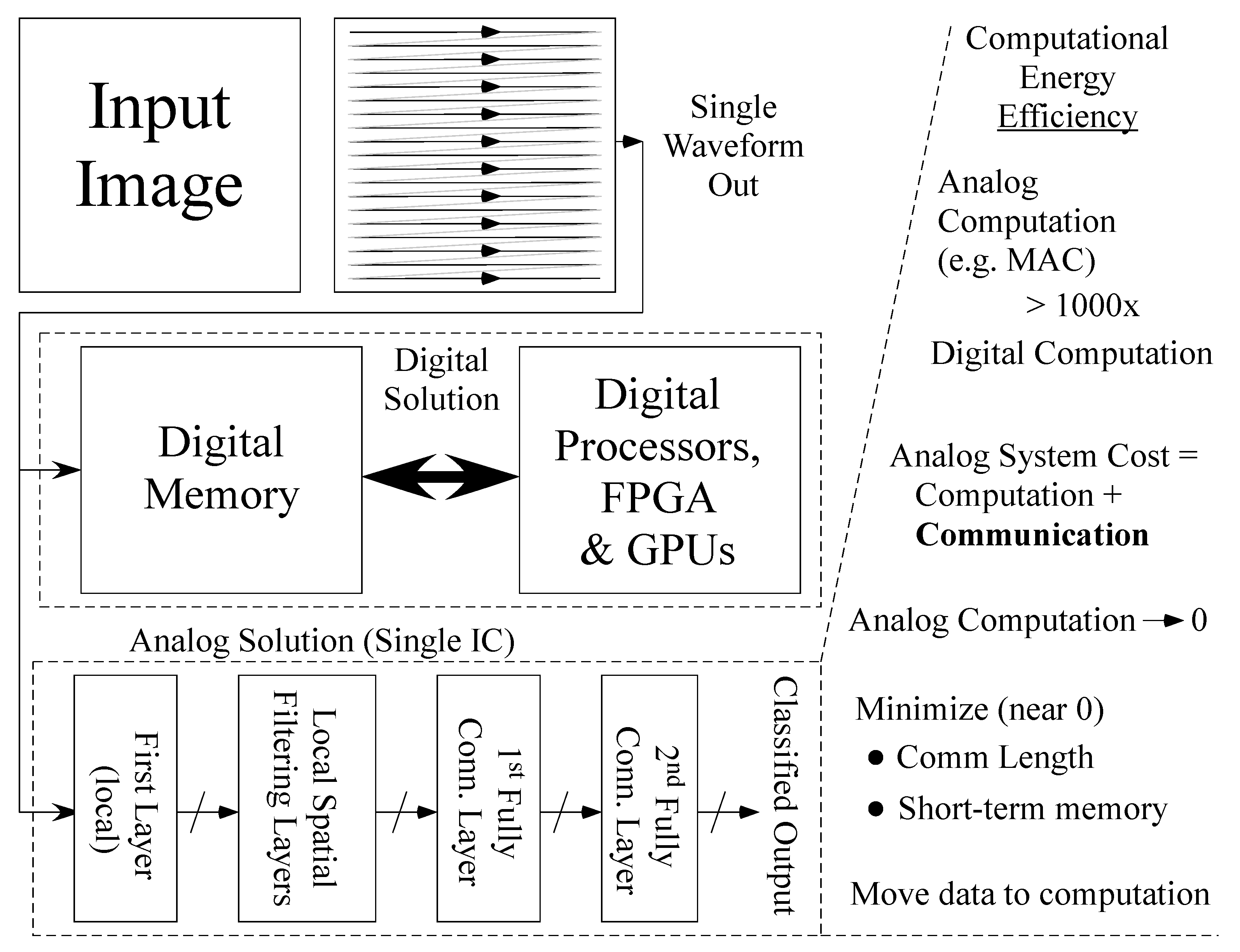
1. Image Classification Requires Analog Architecture Innovations

Our technical approach builds on FG-enabled circuits and analog computation (e.g., [1]), with a particular focus on analog architectures [2] for the NN classification of images for efficient analog computation. This effort both addresses the image-processing classifier architecture coming from a standard imager with a serially scanned input stream of pixels and creates a new paradigm for considering analog architectures based on a synthesizable analog framework, similar to decades-long efforts in digital computation.
Analog computation enables more efficient computation compared to digital computation, as originally hypothesized by Mead (1990) [3]. He predicted that analog computational energy efficiency would improve by 1000× compared to the digital IC design because digital computation requires >1000 transistors, compared to 1 to 2 transistors for basic operations like multiplication or Multiply–Accumulate (MAC) operations. This hypothesis was experimentally proven through Vector–Matrix Multiplication (VMM) in 2004 [4] and continued to be demonstrated over the following two decades (e.g., [1,5]). Computational energy efficiency, the analog equivalent of the power–delay product, balances speed and energy efficiency, where doubling the computation rate requires twice the amount of energy.
Highly energy-efficient computation is a necessary, although not sufficient, condition for developing energy-efficient computations, as one must contend with the architecture that enables these computations, particularly the cost of communication. Analog architectures [2] focuses on the cost of communication and the connected cost of off-chip memory. The more efficient the computing elements, the higher the relative cost of signal communication and memory [6]. One wants the computation to operate at the speed of incoming and outgoing data to minimize the significant cost of intermediate memory stages [2,6]. Applications not respecting these end-to-end computational architecture issues, such as an IC only focusing on building a VMM mesh without the resulting analog system architecture (e.g., Mythic [7]), often struggle to become disruptive market applications. The original development of analog mesh architectures [8], the foundation for synapse crossbar arrays [9], led to one particularly efficient architecture for Neural Network (NN) analog computing, not a universal architecture for all analog applications.
Image processing and image convolutions require significant analog architecture efforts to rearrange data trajectories for image convolutions (Figure 1) when the output of a typical commercial sensor scans each output in a serial stream, one row at a time. Digital approaches deposit the incoming image into a large memory bank due to the ease of downloading an image to memory. Digital computation is far more energetically expensive than analog computation, obscuring the need for minimizing the cost of communication and memory. The 1000×-improved analog computational energy efficiency means that computation is nearly free, where communication and memory access costs make up the system architecture cost. The costs of data communication and memory are always the primary system architecture concerns, moving away from the typical large-processor model in digital architectures [2]. Energy-efficient computational systems require energy-efficient computation with minimized signal communication and short-term memory.
Analog programmability makes these computations practical. Floating-Gate (FG) transistors, having been the leading analog programmable technology arising from the first crossbar techniques [9], led to the creation and development of the field of Compute in Memory (2001) [10], techniques developed entirely in standard CMOS (transistors and capacitors) with no additional process layers or process modification. An FG device provides a free parameter, either as a variable threshold voltage or as a multiplicative weight in subthreshold operation. FG circuits have demonstrated long-term stability (<100 μV change over 10years) and precise, near-single-electron programming (e.g., 14bits in FPAAs [1]), and some FG circuits are only very weakly a function of temperature [11,12,13,14]. FG devices, circuits, and systems have been demonstrated in standard CMOS processes, from 2 μm CMOS [9] through 350nm CMOS [1] to 130nm, 65nm, 40nm [15,16,17], and smaller (e.g., 28nm and 16nm) CMOS nodes [18]. Scaling these systems to smaller CMOS nodes increases the computational energy efficiency compared to digital computation in custom, configurable (e.g., large-scale Field-Programmable Analog Arrays (FPAAs)) [1,19], and neuromorphic [6] areas. Analog FG devices provide FPAA memory elements and routing elements, including computing in routing, achieved by enabling the programming of FG nodes outside of the operating power supply, that are long-term stable and enable programmable circuits with minimal temperature dependence [1]. Analog architecture studies are now beneficial because analog computation is no longer a highly imprecise, noisy, environmentally sensitive, and mismatch-heavy system but has become a robust, programmable, and configurable system often limited by the incoming sensor accuracy.

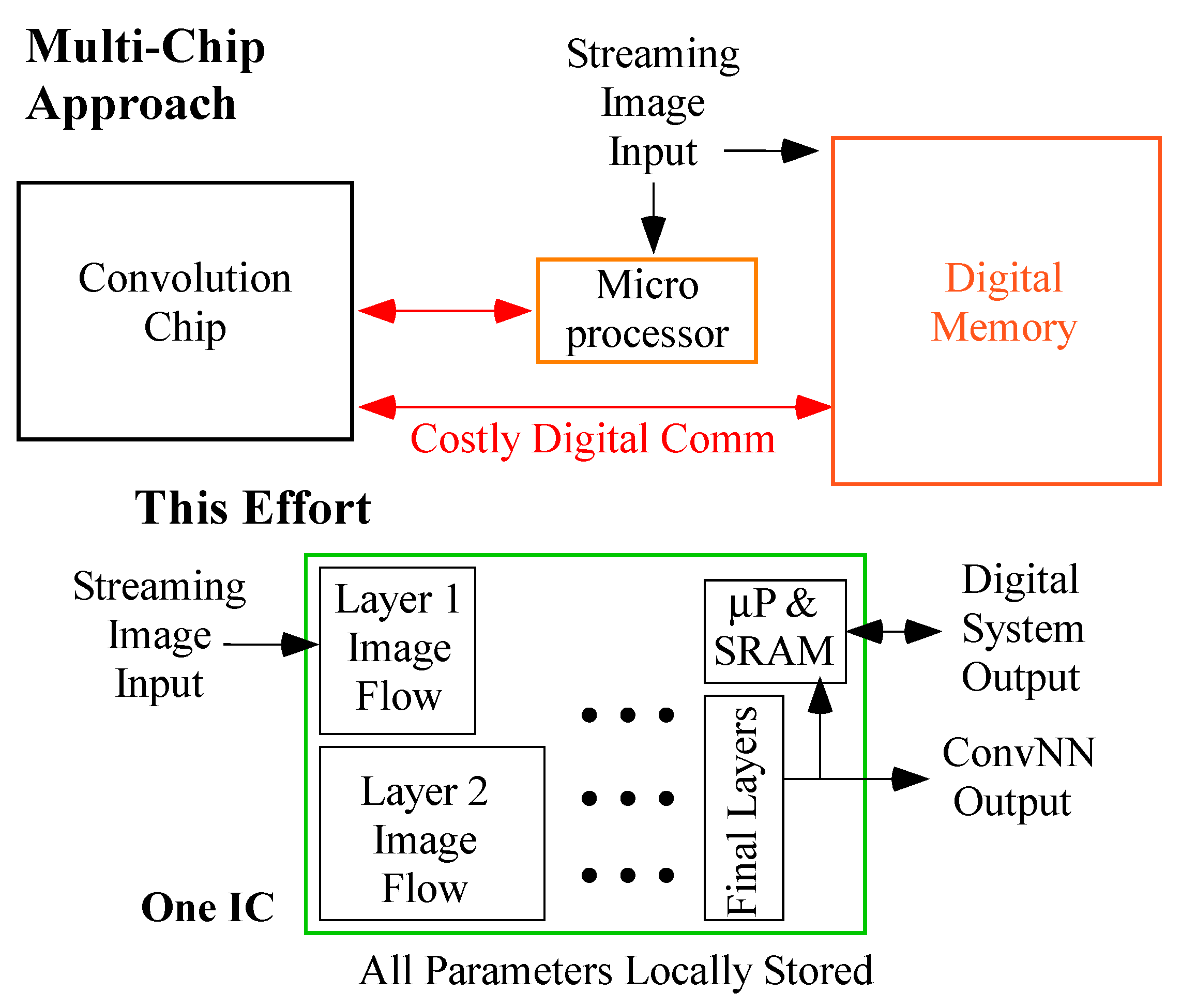
2. Analog Architecture for Convolutional Neural Networks: Minimizing the Cost of Moving Data and Parameters

The cost of moving digital data on- and off-chip to store intermediate products easily increases the system cost by another 1W or more in power (Figure 2). Assuming that a memory chip has zero energy cost, moving data just once, where 1Mpixel at a 10-bit value at a frame rate of 30fps is 300Mbit/s, requires 5μW/Mbit for a very minimal 5pF load (near wirebond level) with a 1V supply (near-minimum chip-to-chip voltage). Moving an image once requires 1.5mW of power. The outputs of the first convolution might require moving 96 images that are subsampled by 4 in width and height 4, resulting in 9mW going into memory (once) and then 9mW coming out of memory (once). Moving partial computations into memory requires even more energy, easily exceeding 1 W for a multilayer architecture.
This article presents the first important example of an analog system that requires considerable analog architecture for image classification (Figure 1), transforming a typical imager input into a classified result using a particular NN algorithm (Figure 3), a convolutional NN (ConvNN). The roots of these algorithms come from the modeling of visual attention [20,21,22,23,24,25,26,27,28,29,30,31,32,33], Hubel and Weisel’s early primate visual cortex measurements and modeling [34,35,36,37,38,39,40,41,42,43,44,45], and the resulting work on the development of spatial receptive fields [46,47,48]. These pyramid structures are similar to the local image correlations developed in visual attention algorithms [27,30]. Often, the first layers of a ConvNN are similar to the adapted solutions (e.g., Principal Component Analysis (PCA) [48]) for the LGN, V1, V2, and next levels in the visual cortex. This creates a number of subsampled image features through local convolutions with the same filter weights. The parameters are small and are not directly dependent on the image size. An image convolution might be for line orientation, edge enhancement, and higher-level features. It is common to see discussions of the receptive fields for the first layer, similar to earlier developments looking at the formation of input receptive fields (e.g., [46,47,48]). Successive subsampling of the structure enables some wider form of position invariance for different image blocks. The ConvNN [49,50,51] has shown significant capabilities over a range of datasets (e.g., CiFAR10 [52], BDD100k [53,54,55]).
A ConvNN typically has two parts to the network (Figure 3). The first part builds up multiple layers of multiple local receptive field computations (also called features), typically arranged as parallel images. The second part is a set of fully connected layers with traditional training of a multiple-layer NN. ConvNN algorithms often optimize the number of network parameters (weights) while allowing the number of computations (MAC operations) to grow quite large. A typical ConvNN algorithm for a 1Mpixel imager (Figure 3) requires 23GMAC. for an image, so running things at 30fps is a 0.7TMAC/s/W operation, with the analog computation conservatively at 10TMAC/(s)/(W) or so. Algorithms of this size typically require between 10M and 50M parameters (10.6M in Figure 3). The critical tradeoff is between increasing the effective size of the receptive field by increasing the number of layers [56] and increasing the per-layer size of the receptive field by decreasing the number of layers. Biological networks have extremely large receptive fields in a single layer, including the first layer of the visual cortex [57].
This single-chip FG-enabled ConvNN architecture (Figure 3 and Figure 4) on a 28nm or smaller CMOS IC benefits from a stable analog circuit capability that, once programmed, will operate with minimal change over the entire IC lifetime. The architecture is based on image-processing algorithms initially developed for FPAA devices and generalized for any analog structure [2,58]. This application is an excellent analog architecture development example (Figure 3), as the primary issue is the architecture and not analog numerics [59], as image convolution applications (e.g., visual attention [27,30], ConvNN [50]) are known to not require significant precision for their calculations, even with a time-sampled algorithm, and therefore, these classes of problems are part of the analog benchmark formulation [60]. Many problems already consider analog numerics (e.g., linear equation solutions [61]).
The recent development of analog synthesis [62] and associated programmable analog standard cells [15,16,18,63], coupled with the long history of FPAA development, makes image classification architecture exploration a relevant technical approach. We expect that a full IC design and measurements for this architecture will be described in the near future, but a final design is beyond the scope of this discussion. These FG standard cells are developed and experimentally measured across many IC processes (350nm, 180nm, 130nm, 65nm, 28nm, 16nm) [15,16,18,63]. Measured programmable analog standard cells for design synthesis significantly reduces the risk of moving between a high-level analog architecture built from multiple analog algorithms, as is typically expected when building large analog computing ICs. Characterization data for standard cell libraries helps the designer decide on the area and performance for a particular architecture design. High-Level Synthesis (HLS) tools that can start from our Python framework have been generalized to target an existing FPAA device and develop the layout file (GDSII) for a custom IC using the standard cell components. These tools improve the design of analog computing systems, significantly reducing human resources and domain expertise due to the lack of automation tools. This article will look at architecture questions that arise when building these ICs in 28nm and 350nm CMOS standard cells [18] and consider particular architectural tradeoffs.
This article focuses on the analog architecture (Figure 3) development required to take an imager sensor output and compute a classified output, eliminating the need for any intermediate data converters and minimizing the need for intermediate memory states. The full architecture discussion starts with moving the data to locally stored parameters (Figure 4 and Figure 5) and enabling core architecture layer (Figure 1) development before discussing the entire architecture opportunity. The following discussion starts with developing the first layer of image convolutions (Figure 4), which sets the foundation for later layers (Section 3), followed by the next level of convolution of multiple images transformed into the next level of images (Section 4), the transformation from multiple images through the first fully connected layer (Section 5), and the final fully connected layers (Section 6).

3. First ConvNN Convolutional Layer

Our architecture (Figure 5) moves the incoming image waveform near the memory for processing. The image convolutions require the data to be moved to locally stored parameters based on a row-by-row scan of an image (Figure 4). The output of an equivalent image stream enables additional convolutions while minimizing the required overhead and communication. The first-layer ConvNN algorithm is the foundation for the remaining ConvNN layers (Figure 5). The first convolutional layer creates multiple images from the local convolution with spatial filter kernels, followed by nonlinear functions. The design must minimize the memory and the distance from the memory to computation. One should not have off-chip memory or even a large bank of on-chip memory. The system block has three primary components: the Arbitrary Waveform Generator (AWG), the input switches and differential-pair modulators, and switches into and out of the integrator blocks.

3.1. Arbitrary Waveform Generator (AWG)

A Floating-Gate (FG) Arbitrary Waveform Generator (AWG) enables the dense and direct playback of a stored sampled analog waveform (e.g., [1]) that allows for presenting the weight value when the input signal is present. The AWG allows a local waveform to be applied right at a multiplying block, minimizing energy requirements due to the small capacitive load. One only needs to sequence a particular AWG (D = 0 for all clocking schemes) when it is being used for a particular computation. The FG programming of the AWG follows similar FG array programming techniques [1,64]. All FG cells should use direct programming to minimize any VT0 mismatch from indirect programming approaches.
Given a typical frame rate (e.g., 30fps) for a typical imager (e.g., 1 Megapixel, 30MSPS), the digital computation operates nearly ideally compared to the rest of the circuit. Increasing this sample rate by 10× results in the same conclusion. The shift register effectively has digital gates driving nearly minimum capacitive loads; one could model the resulting delay as a first-order response, where the time constant would be less than 100 ps for a 65 nm or smaller CMOS node. These D-FF elements can be dynamic latches instead of larger static latches, as static hold is not required given the input clocking rate for these blocks. A dynamic clocking scheme is more likely to be in pitch (Figure 6). These blocks process continually (e.g., scanner), so a 1 output from the shift register should recycle back into the shift register. The same infrastructure can be used for FG programming selection.
Digital computation is effectively ideal for this level of circuit modeling (Figure 7). The speed required for digital computation does not need to be faster than the input data clock rate. For this article’s examples, 30MSPS for a 1MPixel imager results in the fastest clock rate of 30MSPS (30MHz). For a 350nm CMOS process, a 30MHz clock rate for a shift register, particularly a dynamic shift register, is quite easy to achieve, particularly as we have built entire microprocessors (open-source MSP430) in this 350nm CMOS process that clock up to 50MHz [1]. For smaller CMOS processes, these frequencies get easier to achieve. A higher sample rate or a larger image size (>1 MPixel) might eventually strain the digital IC design, although these issues will likely not be the largest issues to consider. The transmission of analog signals at higher clock rates will be a bigger question.
The FG input gate lines during computation are set by a digital multiplexor to the global gate voltage ( V g ) or to V d d , having a similar transient to the earlier digital switching along this gate line. This line is typically short when built with FG-enabled standard cells. The gate line drivers operate at digital speeds converging to V g , which goes to an FG bootstrap current source to minimize temperature fluctuations (setting a ratio versus setting a transistor gate voltage). The time constant for this line is small, given the digital switching conductance. The AWG output line has a parasitic capacitance, primarily due to the drain–source diffusion capacitance ( C d ; m-output shift register is m C d ); the dynamics of this line entirely depend on the output line circuits, as each transistor is effectively a voltage-controlled current source with few additional dynamics or modeling concerns.
Figure 7. A detailed block diagram and timing diagram of the image convolution process for a single-image convolution. This system inputs an image that is communicated one pixel at a time like an imager output and outputs the resulting convoluted image one pixel at a time. This transformation enables multiple layers of similar processing, similar to a ConvNN. The drawing shows a network with no overlap for image convolution (one output per window size) for clarity; additional window outputs for overlapping windows require additional integrator stages and multiple AWG outputs and differential pairs. Three shift registers (one in the AWG) select the right weight data to be processed at the right output (integrator module) for the image computation, minimizing the amount of data storage (the number of integrator elements). Nonlinear elements, such as WTA, sigmoidal, and ReLU blocks, can be added before the multiplexing of a single output.
Jlpea 15 00037 g007

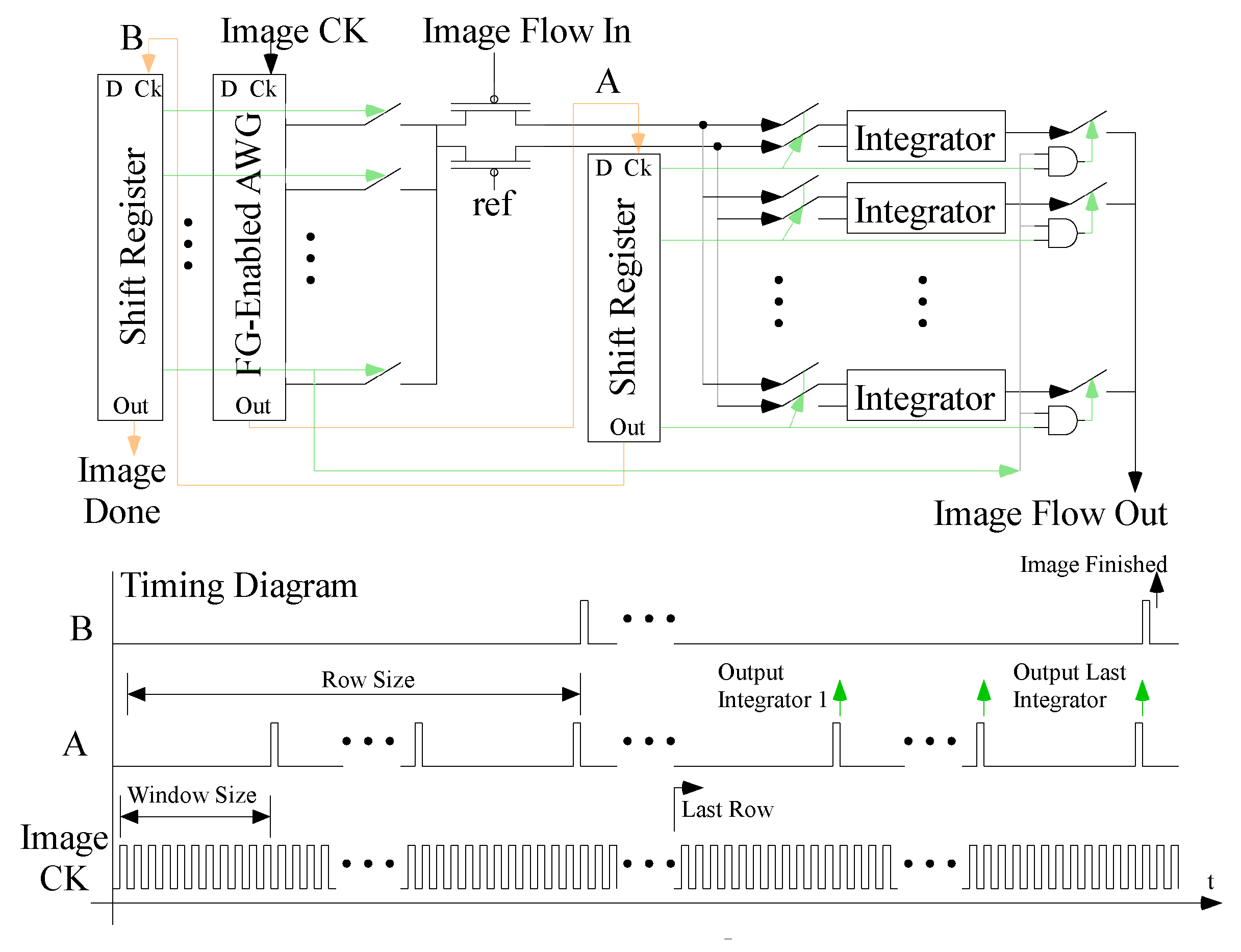
3.2. The Full System for the First Layer

The core system correlates the input signal with the desired weight value encoded as a waveform (AWG block), first pixel by pixel and then on a slower timescale, row by row. Although the AWG block and resulting outputs are straightforward, the remaining computation requires some consideration. The weights are reused for each subblock of the original image, effectively repeating the played correlating waveform of the weights (Figure 4). The AWG waveform output current goes through a source-coupled transistor pair (Figure 7), enabling the modulation of the scanned input image signal. Clocking schemes (Figure 7) should be as local as possible to minimize communication and minimize clocking complexity. The shift registers can be dynamic shift registers, as the signals are always moving during computation, significantly reducing the circuit complexity. The “pause” and “Sel” are line-dependent clock-switching operations that roll the data in the right direction. The output of these integrator elements can be followed by a Sigmoid, Relu, or other nonlinear function (WTA, max pool) (e.g., [62]).
The detailed circuit (Figure 8) for the system picture (Figure 7) provides enough detail to model the resulting circuit components, enabling system-level macromodeling.
Differential-pair modulator: This circuit component finds the time constant to the source (Va) of the differential pair and the output of this differential pair. The AWG selection switches (typically T-gates) connect to either the source node (Figure 8) or to a cascode node connected to the reference ( V r e f 1 ) node (shunted to GND); therefore, the current is always flowing and flowing near the same potential. Effectively, Va is an approximately first-order system of the signal current (I) along the entire row capacitance (mCd) and the subthreshold source conductance of the differential pair or cascode ( U T / I ) with a time constant and/or required bias current:
m C d d V a d t I ( t ) I t h , p e ( κ ( V d d V r e f 1 ) ( V d d V a ) ) / U T
τ d V a d t U T I ( t ) I b i a s e Δ V a
τ = m C d U T I b i a s , I b i a s = m C d U T τ
where I b i a s is the normalized current for the AWG current outputs and is a function of the bias voltages. V a needs to be 100mV or more below Vdd. For C d = 0.5fF (typical of larger-linewidth CMOS processes) for a 20-stage AWG, setting τ = 10ns for a 30MSPS signal results in I = 25 nA. The resulting value for Va sets the signal modulation (Figure 8) into differential output currents (I+, I) for the next stage. The sampled current source from the AWG goes directly into a differential pair for modulation from the incoming image. The differential-pair modulation can be a single input voltage or a balanced input voltage around V r e f 1 ; the input can be an FG input if a larger input signal range (larger linear range) is desired for the computation. Having an FG differential pair enables a large linear range and potential offset control. Differential signaling results in a wider linear range, although it requires additional signal handling. The signal comes from a waveform generated by stored input currents, requiring one FG per storage parameter. An additional offset current can enable some signal representations, such as four-quadrant weight times input signal formulations (Figure 9).
The macromodeling of this computation considers the edge signal settling for a discrete sample of the image or subimage rate. Analytically solving and predicting the solution at the sample edge boundaries is sufficient and simplifies the modeling. The switching going into the Va node is an LPF that is under control on these timescales. Typically less than 3% of the previous signal for aggressive sampling (3 τ) shows up in the new signal, so one could macromodel it as an LPF on a sequence of coefficients. Slightly higher biases eliminate the issue almost entirely, resulting in a smaller τ for the image sample rate.
Selecting the integrator block: The differential output current is then directed into one of multiple single or differential current integrators, with the output signal buffered to the next computation layer (Figure 8). The differential current is integrated for part of the cycle. An amplifier will be required to drive the output voltage of the integrator block, as well as diminish the effect of some parasitic capacitances and match the desired capacitors. Modeling the integrator output voltage (Vout) through an amplifier (single-ended, Case B in Figure 8) after a reset results in
C 1 d V + d t = I + , C 1 d ( V V o u t ) d t = I , V o u t A v ( V + V )
C 1 d ( V + V V o u t ) d t = C 1 ( 1 + 1 A v ) d V o u t d t = I + I ,
This approach can extend to a balanced differential output (Case C in Figure 8). Additional transformations are possible after these nodes, such as a tanh, Relu, WTA, subsampling, or other pooling. After the target subframe has been completed, the integrating amplifier outputs are sampled in sequence. The integrator only drives through the switch at the end of the computation and does not affect the integration computation. An output buffer minimizes the impact of the switches in driving to the next image transform layers. The amplifiers would have FG biases.
These integration windows set the required bias currents, and that sets the average current level for the AWG block. The bias current (Ibias) is a function (Figure 10) of the imager size, frame rate, and receptive field overlap (K × K). The required currents will be subthreshold currents (less than 1 μA), simplifying the FG programming of these elements and allowing the FG measurements to focus on this narrower range of computation [13].
The front-end switches going into the integrator clear the integrator. Eliminating Charge injection adds additional complexity to the timing diagram. One side of the capacitor switches is released early to have a constant charge injection voltages. The nearly zero differential charge injection effect reducing the need for any modeling in that part of the macromodeling process. The experimentally measured accuracy for sampled signals is better than one would expect from SPICE simulations [65]. The integrating capacitor mismatch ( C 1 ) affects both the integration results and the timing mismatches. The <0.1–1% C 1 mismatch between capacitors is well within the 8–10-bit range for the image convolutions before the nonlinear element. This modeling moves the transistor model from a level = 2 into a single level = 1 model for the full modulator block to the integrator.

4. Additional Convolutional Layers

Implementing additional layers of convolutional NN blocks (Figure 11 and Figure 12) requires the combination of input image streams from previous convolutions and creating, through convolutions and nonlinear operations, a set of output image streams. A two-dimensional array of image stream convolutional blocks enables this computation, where signal aggregation occurs over a row of blocks instead of a single block.
This architecture directly scales as a mesh of image convolution architectures that map well in a two-dimensional architecture (Figure 12). The core blocks created in the first layer continue to be reused for each additional layer and effectively become standard blocks derived from programmable analog standard cells. Local clocking control further enables these multi-dimensional convolution expansions.
Figure 12. The block diagram for the physical implementation of multiple layers of image streams being processed. The resulting architecture using these image streams is effectively a mesh architecture, minimizing data communication through the processing of the ConvNN implementation, as well as showing that the implementation easily fits into a two-dimensional architecture.
Jlpea 15 00037 g012

5. Convolution to First Fully Connected Layer

The first fully connected layer must take in multiple small images to be correlated with weight parameters into a single vector output (Figure 13). The weights required effectively create a fully connected network with many AWGs for each input image. The output vector will be computed at the frame rate of the input image (30fps → 30SPS). The programmed AWG currents will be significantly smaller than previous stages to match the lower processing speed. These blocks follow classic Neural Network (NN) layer formulations, greatly simplifying the architecture into a meta-level mesh architecture.

6. Fully Connected Layers

Additional fully connected layers are typical VMM computations followed by a nonlinear termination, as these mesh architectures are the optimal design for these computations. Computation will be at the image frame rate.

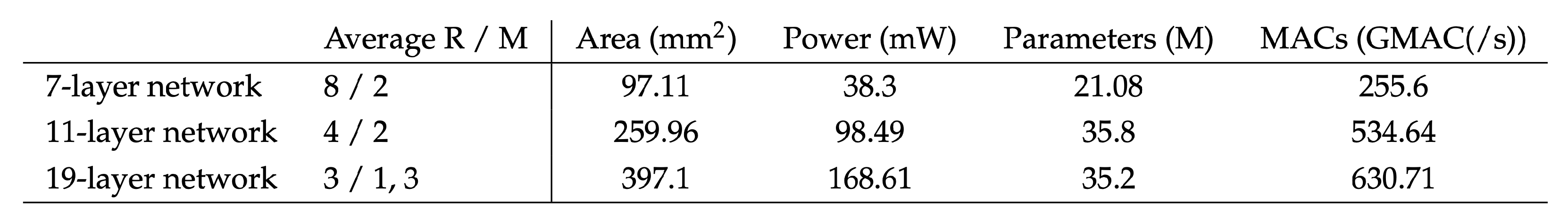
7. Analog ConvNN System Analysis

Given the entire architecture approach, one can evaluate the expected complexities (Figure 3) for a single analog IC architecture (1M input, six layers) to compute a ConvNN with minimal intermediate storage elements and communication. The input image is a scan of pixels on the input sensor. Each layer creates multiple additional images that provide metrics (e.g., line orientation) in that processing layer. The architecture requires four different processing types. The first layer creates a number of new images from the input image, resulting from different image convolutions. Most additional convolutional layers require convolving multiple input images into a number of output images. One layer performs a convolution that flattens multiple input images into a single vector. The following remaining output layers are typical mesh-based NN layers for converging to a desired output vector. For this 1 Mpixel computation, the first layer has a step of 4, and the 2nd–4th layers have a step of 2. The input clock frequency decreases with the layer, corresponding to a proportionally lower AWG programmed current to minimize energy requirements. FG MOS transistors can be programmed with over 8 magnitudes of bias currents [13]. This energy estimate would extrapolate to many deep ConvNN networks (50 to 100 layers) using <1W of power.
Given the architecture opportunities, tradeoffs in the neural networks should be considered, given the on-chip analog computation. The programmable high-precision (>8 bits) analog weights and the resulting computation go in a different direction from many of the digital components’ (e.g., GPU) precision towards 8-, 4-, and even 2-bit operations. The architecture does not require any ADCs or DACs, unless users want to data-log intermediate measurement results, typically a rare operation used when debugging an algorithm. One tradeoff is between the length of the AWG and the number of integrators in a single block; a longer-length AWG and the resulting 2-D receptive field result in fewer integrator blocks. The integrator blocks typically require more area than the AWG for typical implementations. This larger 2-D receptive field also entails tradeoffs between increasing the AWG and reducing the number of required NN layers.

7.1. Intractable System-Level SPICE Simulations

The cost of a full-system simulation to understand image behavior translates to a nearly intractable simulation for 1Mpixel and larger imagers, therefore requiring macromodeling for full-system understanding. The cost of performing a SPICE-level simulation of this system for a 1Mpixel, seven-layer, 50M-parameter-level ConvNN image classifier at 30fps with 20× oversampling for a second of image data requires roughly 400T (4 × 10¹⁴) transistor evaluations. Assuming a very high-performance digital computing engine, one expects 10 μs per transistor evaluation, resulting in 400Ms (4 × 10⁸s), or 127 years. Even 2000 multi-processor nodes with memory and perfect communication would require 23 physical days for one single computation. Simulating a small system typically misses most of the architecture-level issues, and given that architecture issues are a critical concern, a typical SPICE-level simulation is essential. The ability to perform a fast, high-level analog simulation is an open problem that will hopefully be solved in the near future [66].

7.2. Robust Analog Computation in the Presence of Environmental Conditions

Analog computation can have long-term stability and be weakly affected by environmental factors. The wide use of SoC FPAAs requires a robust analog circuit infrastructure [1] that would be shared for this FPAA structure. The FG-device- and circuit-enabled Neural Network and related concepts have been stable from their inception [9], through adaptive NNs [67], through VMM + WTA classifiers [1], and beyond.
The elimination of mismatches through precise programming is an essential part of any analog computational architecture. FG circuits have experimentally demonstrated long-term stability and long-term (industrial maximum standard of 10 years) < 100 μV precise, near-single-electron programming (e.g., 14 bits in FPAAs [1,13]). FG devices have been experimentally demonstrated in standard CMOSs in every CMOS process, from 16nm CMOS (FinFETs) through 2 μ CMOS devices. This FG-enabled implementation has no stochastic conductance fluctuations, typical of RRAM and other nonvolatile devices.
After eliminating transistor mismatch through precise programming, potential environmental issues can be addressed. Some FG circuits are only a weak function of temperature [11,12,13,14]; a programmable bootstrap current source would have 200 ppm [12], and offsets under 1 mV are compensated over a wide temperature range (>100K range) [11]. VMM computations had 8–10-bit accuracy over a wide temperature range (>50K range) [5]. FG programming can eliminate mismatch, and this has the side benefit of further reducing any Vdd variation effects. Although some physical implementations are highly temperature-sensitive (e.g., only operating over a 1–2 C range [68]), these are the circuit design choices when there are alternative circuits with weak temperature dependence [14]. This architecture tends to be insensitive to power supply voltage changes. Besides the careful FG-enabled bootstrap current sources setting the core circuitry, all pFET FG devices and terminals (e.g., source and well) are referenced to the operating Vdd. As the supply moves, so does the FG, with no overall circuit effect, as seen in multiple FG implementations (e.g., [69]).
In practice, many mismatched-removed analog circuits (e.g., FG programming) routinely have 50–80 dB (8–12-bit) SNR (e.g., [1]). In transistor-based circuits, noise is effectively a combination of thermal noise and Flicker (1/f) noise [70] and will often practically depend on capacitance sizes (kT/C noise). Flicker noise is typically seen at lower frequencies and is only an issue in the integrator blocks. Analog numerics [59] and multiple circuits have been measured with SNRs of 10 bits or higher for many years (BPF, VMM [5], etc.).
Multiple demonstrations of these programmable capabilities across multiple IC measurements are not only essential for analog computation but are the way to perform a careful analog architecture study without having full-system-level IC fabrication measurements. An important goal of these efforts is to enable similar well-founded architecture studies going forward. The system macromodeling becomes like an idealized approach as the analog IC programming and techniques for good temperature behavior are well controlled.

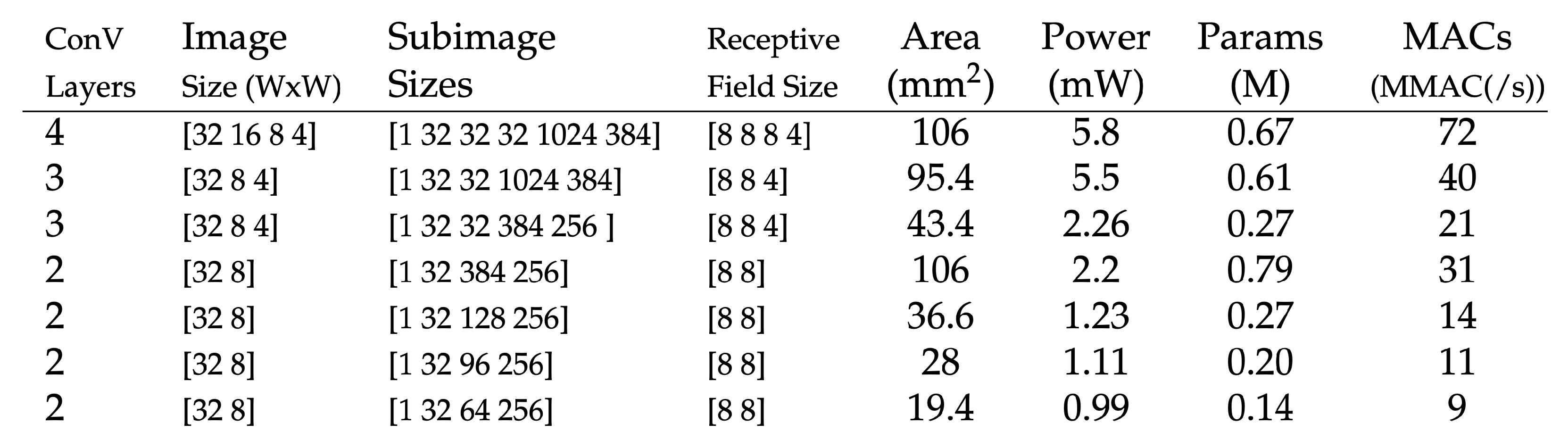
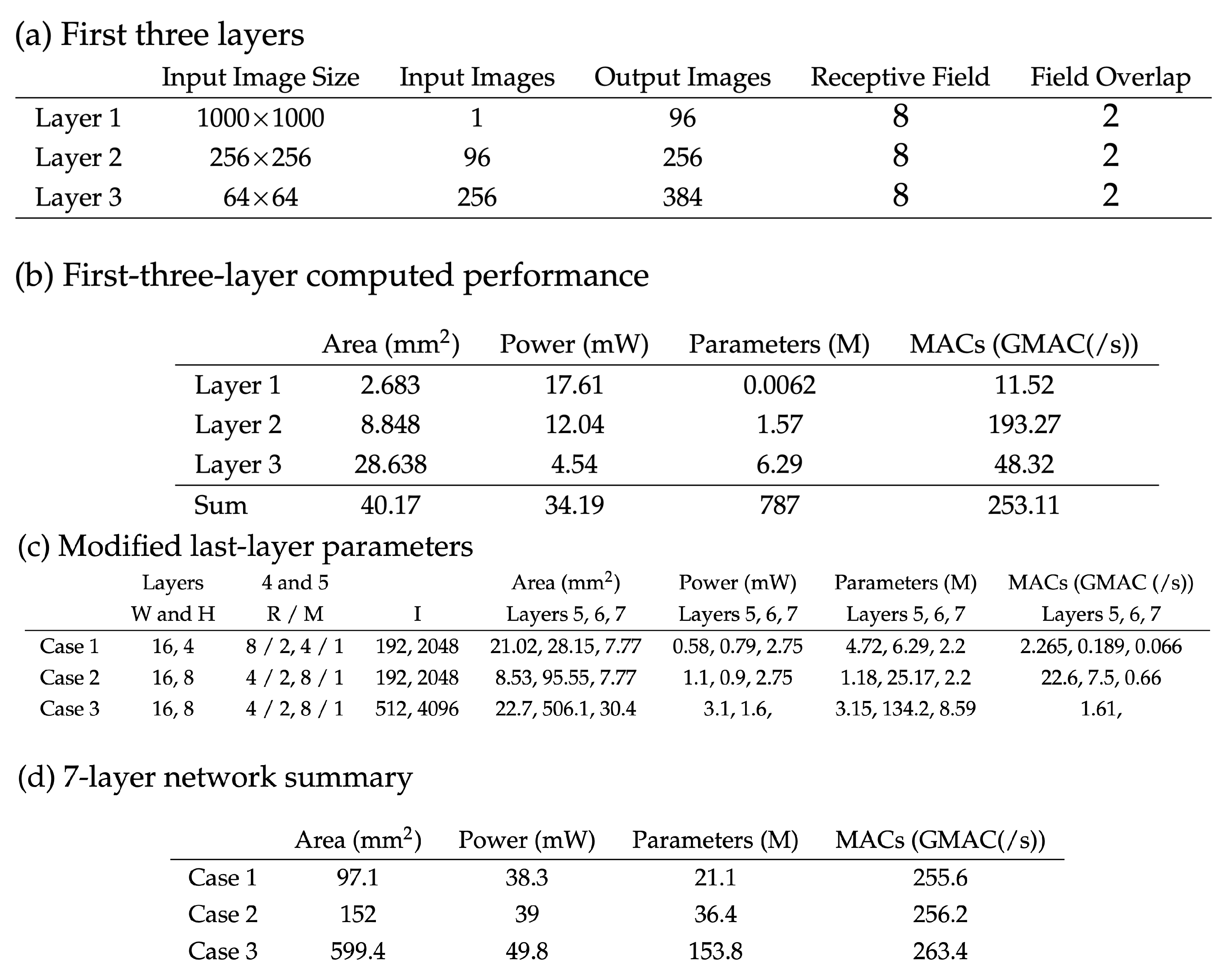
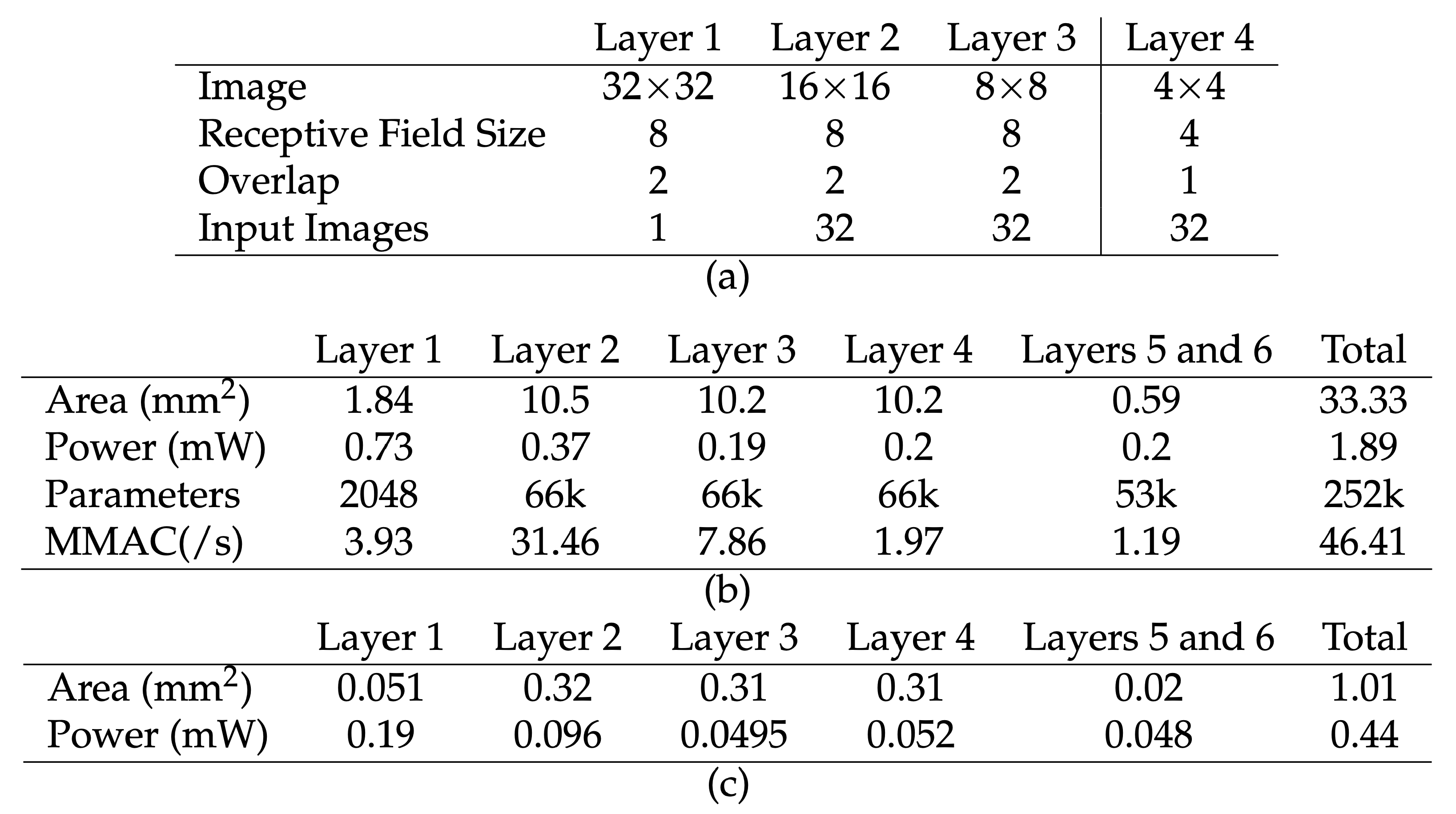
7.3. Detailed System Analysis for a Convolutional Network Layer

The detailed architecture can be modeled for different image sizes, frame rates, receptive fields, and resulting overlaps. The process from a single image input convolutional block to a single convolutional block output with a given imager sampling time (T), image size (width (W) × height (H)), receptive field (kernel) size (K), and receptive field spatial sampling overlap ( K o v )/outputs per receptive field (M) results in a single-stage delay of W × K × T , while the pipelined delay is negligible. Typically, one has many input subimages (S) for the convolution. The convolution block requires
  • K o v of K × K AWG blocks;
  • ( D / K ) M 2 integrators;
  • M 2 K o v Diff-pair;
  • 2R + (W/K) M shift register blocks.
For a layer with R = 12, W × H = 1000 × 1000 running at 30fps, and T = 33ns (30MPS input rate), the resulting single-sample delay would be roughly 0.3 ms. If there are multiple images, the results are output in parallel, so just one delay value for the layer. The delay from the pipelined computation is nearly zero.
The required area is primarily a combination of the AWG system, which has an R × R weight size; the FG multipliers; the controlling shift registers; and the integrator modules. The resulting convolutional area (Aconv) becomes
A c o n v = A d i r e c t K 2 / 8 + A m o d M 2 K o v + A i n t e g ( W / K ) M 2 + A s h i f t ( 2 K + ( W / K ) M )
given the area of the programmable analog standard cell (e.g., 130 nm and 65 nm [15,16]), the direct 4 × 2 SWC cell (Adirect), the modulator as a modified FG input differential pair (Amod), the integrator cell (Ainteg), and the shift register cell (Ashift). We will look at these examples for 28nm and 350nm CMOS standard cells, and the results will be published in the near future. Assuming a typical 28nm CMOS process, one can estimate the resulting architecture size for this technology node; by using standard cells for another technology node, one can equally predict the resulting die area (Figure 14).
The required energy for this convolutional structure depends on the programmed currents that charge and discharge from the required capacitors. The energy does not include the energy for the single-output buffer, as that structure is dependent on the routing for the output load. The power for the AWG computation is
P 1 = I b i a s V d d = I K 2 C d V d d U T τ
which requires current from all AWG rows because the circuit switches between active rows. The source–drain capacitance ( C d ) for a single stage sets the response. The differential amplifier modulator power is already included in this total power. The integrator power models the amplifier, addressing the output capacitance as well as the feedback capacitance,
P 2 = I b i a s V d d = ( C 1 + C L ) V d d 2 U T κ τ 1 ,
modeling the integrator capacitance ( C 1 ) and load capacitance ( C L ). The switch resistance would be smaller than the driving current, so it is negligible in this analysis. The power required for the shift register with the resulting small capacitors is negligible compared to these other computations. The total consumed power would be
P = K P 1 + ( W / K ) M 2 P 2 ; P = K 2 C d V d d U T τ + ( W / K ) M 2 ( C 1 + C L ) V d d 2 U T κ τ 1
and assuming τ and τ 1 due to the same clock, we get
P = V d d U T τ R 2 C d + ( W / K ) M 2 ( C 1 + C L ) 2 κ ,
showing the total capacitive load for the computation. FG elements are minimally programmed for the resulting delay. This model allows tradeoffs in terms of R (Figure 14).
Figure 14. The tradeoff of the estimated area and power with the receptive field size (R). The plots show area and power, as well as the inverse of area and power. Showing the inverse of area and power shows the breakpoint for trading off R for improvements in area and power. A larger R tends to also decrease the number of layers in the ConvNN structure. The input image was W × H = 1000 × 1000 with the following parameters: S = 1, M = 2, τ = 10ns for 30MSPS, C d = 1fF (changing the capacitance to 0.25fF had a nearly negligible effect), C L = 50fF, C 1 = 50fF, and κ p = 0.75. V d d is 1V. Area and 1/area computational estimates as well as power and 1/power computational estimates show the strong impact of integrator elements and demonstrate that increasing the receptive field size significantly decreases the required integrator area and power.
Jlpea 15 00037 g014
The tradeoff with K for area and power leans strongly towards larger R for an individual correlation (Figure 14), not to mention that it likely reduces the number of required layers for the implementation. The last layers, which are flattened NN layers, have a straightforward tradeoff in terms of size and power. Ideally, one does not want a long sequence of minimal-size (3 × 3 receptive field) convolutions, and the experience from visual attention networks shows that networks can have fewer layers when using larger receptive fields. These discussions were clear in the earliest of NN implementations, where multiple layers were used with small receptive fields to build layers with larger receptive fields, trading off the receptive field depth and weight complexity (and number of levels) with the number of layers (e.g., [50]). Early approaches like edge detection still work when only spanning part of the image for a robust kernel, enabling similar translational invariance.
This model enables the modeling of an entire network in terms of its area, power cost, and non-pipelined delay given a target ConvNN architecture (Figure 15). Images are often subsampled for each increasing layer, resulting in a lower sample rate and typically lower power for each resulting layer. A 1M image that decreases to a 512 × 512 image goes from 30MSPS (30fps frame rate) to 7.5MSPS (same input frame rate). The first layers would cost the most in energy because they have the highest initial frame rate, etc.
From this modeling process, one can see the effects of different architectures on area, power, network parameters, and computations (Figure 15); the primary effect is the need to minimize the number of integrating stages, where more parameters with fewer integrating stages result in a more efficient (area and power) implementation. One can start by considering a seven-layer ConvNN implementation with a wide receptive field with common first-three-layer implementations (Figure 15), typically corresponding to the particular system’s LGN, V1, and V2 layers. The cost of the first layer and the resulting number of integrator blocks operating at the full sample rate can be seen by the high energy cost of Layer 1 (17.61mW) with 96 outputs vs. the cost of Layer 2 (12.04mW), which has 256 outputs; the integrators and the number of outputs set the implementation cost. The resulting higher energy results in a lower overall energy efficiency for the first layer due to the integrator cost. Changing the receptive field width or increasing the number of output images in the fifth layer can cause significant increases in energy and area, sometimes enough to make a full ConvNN impractical on a single IC. A simple shift in the receptive fields in the fourth and fifth layers (Case 1 to Case 2) resulted in a 1.73× parameter increase and a 1.57× area increase. Increasing the number of layer-5 output lines with this change resulted in a 4.22× parameter increase and a 3.9429× area increase.
Many ConvNN implementations use 25–50 layers or more, such as what one sees in ResNet networks [71]. These ConvNNs use small receptive fields (3×3) to parallel efficient digital pyramid computations (e.g., [71]) to create groups of receptive fields similar to attention processing, as subsampling only occurs in groups of layers, as seen previously. The attention networks originally used these pyramid computations to computing spatial receptive fields (difference of Gaussians) for efficient low-bit precision FPGA implementation [30,31,32]. As many operations are considered convolutional layers, a more careful definition would be that a layer performs a spatial convolution and spatial compression before a set of nonlinear operations ( ReLU, Softmax) that can extend over multiple pixels.
How does modifying the receptive field change the resulting network size? The human visual system, which is far more capable than any ConvNN implementation, has fewer than 50 layers. A careful study of this approach would require training multiple networks, and that would be beyond the scope of this discussion at this time. The resulting architecture significantly increases in area and power when moving towards smaller receptive fields and many layers (Figure 16), typical of performing a pyramid computation to build up a desired receptive field. When changing our networks from wider receptive fields to many layers of narrow receptive fields (Figure 16), one does not have a large change in the number of parameters, but the number of layers changes significantly. The larger receptive fields require higher-resolution computations, both in the weight multiplication to build more complex receptive fields and in the intermediate computations before the nonlinear functions (ReLU, SoftMax). The analog computation described in this discussion enables both higher stored precision as well as higher computation precision, resulting in a lower number of layers, and potentially resulting in more manageable training requirements, as well as reducing the required network complexity (as in ResNet architectures).
Using a different programmable standard cell process (350nm compared with 28nm CMOS) illustrates further tradeoffs between these structures. As a 350nm CMOS implementation would not realistically handle a 1MPixel model, one might look at a smaller ConvNN input, such as a 32 × 32 Cifar model (10 outputs). This circuit model can fit in a 5.7mm × 5.7mm die (Figure 17). If one uses 28nm CMOS standard cells, the area (33×) and power (4×) decrease. Further tradeoffs for a (Figure 18) 350nm CMOS mode are possible to build a classifier that can reach a wide range of projected die sizes, including the tradeoff on the number of convolutional layers.

8. Summary and Discussion

Architecture design is essential, as energy-efficient analog computational elements are not sufficient for all analog problems. All weights are stored on-chip and locally near the components as part of the Arbitrary Waveform Generator (AWG). No data is loaded from anywhere else. No intermediate ADCs are required for any of the intermediate data. Data converter components are large; the resulting memory would be costly, and the resulting accumulation in digital form would make the accuracy even lower. Analog programmability is both necessary and achievable in an analog CMOS. The approach minimizes data movement throughout the chip. This original architecture approach originally appeared as an FPAA concept and an is important analog benchmark problem [60].
Figure 18. Potential network tradeoffs for a 350 nm CMOS ConvNN. Networks are all assumed to run at 30fps when implementing a Cifar10 problem with single-input intensity (grayscale) images with a 32 × 32 input image and classification into 10 categories. The last item would fit within an area smaller than 20mm2 (4.3mm × 4.3mm).
Jlpea 15 00037 g018
The following subsections discuss multiple topics resulting from this architectural work, including a summary of the opportunities for on-chip learning (Section 8.1) as well as a comparison of these architectures with architectures heavily relying on external digital memory (Section 8.2) and a comparison with other analog architectures (Section 8.3).

8.1. Opportunities for On-Chip ConvNN Learning

Although this discussion does not focus on learning for these networks, this architecture discussion invites the question of how to design efficient on-chip learning algorithms, enabling the local, personalized training of these networks and reducing the energy required for training and decreasing the high energy load of commercial servers [72]. A full ConvNN learning architecture is beyond the scope of this article, but an overview of what is possible sets the table for future discussions.
The straightforward part of this architecture is the learning in the last two layers, as those flattened vector layers could be trained using continuous-time LMS (and backprop) FG learning (e.g., [2,67]). Continuous-time adaptations, starting from early adaptive systems with discrete components (e.g., [73]), have superior convergence compared to discrete adaptations with fewer constraints for convergence [74] and can have adaptations continue without worrying about numerical instabilities for any adaptation time [59].
The initial training for the first layers would use local PCA or Independent Component Analysis (ICA) to find the weights for early convolutional layers, as demonstrated previously [48]. The first layer would use PCA/ICA, say, over the 11×11 receptive field images that are expanded into a 121-length vector, and the initial weights would be the largest or most relevant 96 cases (of 121). The next layer would take the resulting 96 subimages, which are broken up into 5 × 5 images and expanded into a 25-length vector with all 96 subimages, resulting in a 2400-length vector. One would perform a PCA of these subimages and take the most significant 256 of them, where one has the resulting 5 × 5 block for each subimage, again relating to the subimage formation seen in multiple cases ([48,75]). The intermediate layer is similar to the output of the last two layers, but the input would be more typical of the LMS layers. The approach for these layers might be to have a custom analog IC PCA/ICA computing engine for this computation (e.g., [76,77,78,79,80,81,82]) or a parallel digital computation, evolving the weights starting from the first layer to the last convolutional layer, as is typical for theoretical formulations [48]. The resulting eigenvectors give the starting receptive fields and are likely sufficient for most ConvNN algorithms, particularly as the specifics of early layers that project to a high-dimensional basis can have high variability for good network performance (e.g., [83,84]).
If one wanted to perform additional LMS training of the input convolutional layers, one would modify the AWG to enable local adaptation. When a weight is being selected, there is a current in one pFET device, so modulating the drain voltage during injection with the input signal would give the desired LMS adaptation. This approach would use indirect pFET injection using a second pFET transistor in the AWG to modify the injection current during learning. Tunneling can be used to normalize the response in multiple approaches. The learning rate can be arbitrarily slow to average over an entire epoch. One must be careful with long training sequences in a form typical of digital training, as training is a sampled time system, although with some properties of continuous ODE training. The last layers can continue to continuously adapt while adapting a particular convolutional layer.

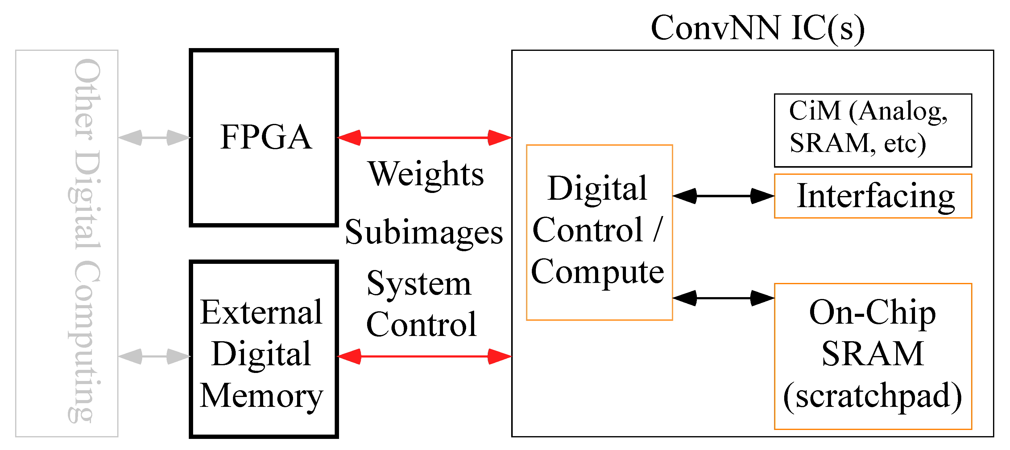
8.2. External Digital Memory ConvNN Architectures

The often used analog computing approach that liberally uses digital memory loses most of the analog computation advantages because of communication costs, as well as data conversion costs. The heavy digital infrastructure couples a small analog computation block with a Huge memory bank that stores the input and significant digital control to this analog co-processor. Storing a full image in the memory and operating on that memory creates a costly solution, whether in the analog or digital space. Routing lines create additional communication lines, resulting in additional costs, particularly in digital approaches. Digital memory for storing intermediate results also results in ADC and DAC energy and complexity costs in the algorithm. When solving problems that require moderate weight precision (>4 bits), all of these costs are significant. Some approaches simply use an analog VMM-type array, either entirely in Si [85] or with memresistive devices [86], where the analog computation is performed by a small co-processor with a wide range of digital circuitry. In these cases, the analog computation improves performance, but the digital architecture still dramatically limits what is possible. Some architectures can be improved by moving the digital memory closer to the analog computation [87], including through efficient DAC structures [88], although these techniques are limited by digital communication and data storage.
Although the use of external digital memory creates significant energy and complexity costs for a system, it is still the dominant implementation approach. In all of these cases, the cost of the external FPGA (e.g., [89]) and/or external memory (Figure 19) is never considered, nor is the cost of communicating with these systems; sometimes the system requires a host computer (e.g., [89]). One incurs the cost of moving intermediate subimages and moving weights as well as other parameters throughout the computation. The approach is improved by having an on-chip microprocessor (e.g., ARM Cortex M [90]) if all of the memory for the microprocessor and all of the processing is available on-chip, which rarely happens. Scratchpad SRAM does reduce these issues (e.g., [90,91]), but to a level where it reduces off-chip communication; all off-chip intermediate computation must be eliminated, even for mostly digital computation. The cost of requiring off-chip memory (e.g., [89,90,91]) far exceeds that of all other metrics, making any comparison of a complete on-chip structure with local communication (this work) with such structures not meaningful. Until these aspects are seriously approached, any real metric comparisons will be dominated by these external components. Some have claimed that early low-power image-processing implementations suffered from this situation [92,93,94,95,96,97]. Often we have no data on the resulting system cost, as it is not given in sufficient detail to evaluate. Our approach entirely avoided these issues for large-size images, only requiring low-speed digital outputs of the image class(es).
Some users will extend the heavy use of external memories to enable larger computational functions, including how a given component technology, such as a VMM CiM block (Figure 19), could be used for image processing. When used as a demonstration of potential image computational capability [98], these techniques are justified. If one makes claims about system specifications of energy efficiency and efficient architecture approaches [99,100], such claims and the resulting specifications are stretched beyond what is reasonable, as including the digital infrastructure is necessary as well as defeats the positive aspects of what is being demonstrated. These techniques lead to the misguided approach of considering the analog CiM as a co-processor with high-cost data converters between steps, rather than using an architecture that optimally uses the analog and digital components for their advantages. In this discussion, we only have VMM CiM computation for the final layers; in the other layers with VMM-related computations & the AWG block is a small and efficient piece of the wider computational architecture.
Often these structures are designed with very low-precision components and computation (e.g., 1 to 4 bits), using many NN layers to enable a higher-precision classifier. One might use a lower bit precision because the storage and computing device (e.g., synapse) components only have a limited precision (e.g., [99,100]), or one is considering a digital form of CiM with a limited form of analog computation [89,90,91] for intermediate distributed computing [101]. In general, IC designs do not start with reading the sensor output, but rather a parallel input of the vectors, already assuming there is memory for data reordering [89,90,91], missing an important architectural issue. The memory bottleneck, usually downplayed in such implementations, usually gets mentioned, such as internal transfers in the IC accounting for more than 50% of the energy requirements [89] or the high amount of energy required for off-chip DRAM access [91]. Often VMM operations have only up to 4-bit outputs, requiring small 4-bit flash structures (e.g., [91]), DACs and ADCs for conversions (e.g., [90]), or other simple nonlinearities to move the data back to a digital format. The assumption is that the output images, often just labeled as activation functions [89,91], are a single bit, and rarely more than 4 bits. The situation gets more complicated when dealing with nanodevice structures (e.g., PCM), as one requires DACs to supply each input signal, requiring off-chip or on-chip memory access, and also incurs costs in reading the image output from the image sensor and storing it in memory before transferring it to the DACs (e.g., [99]). This effort not only excludes these resolution constraints for a full analog architecture but also keeps all processing on a single IC with only very local on-chip communication for these analog signals.
A large number of intermediate pyramid layers, originally developed for putting attention networks on FPGA devices [30,31,32], enable useful low-bit input, weight, and output resolution. Attention networks used multiple layers of small receptive fields (e.g., three) with minimal overlaps (e.g., one) in what was drawn as a pyramid [30] for computing spatial convolutions for the difference-of-Gaussian weighting for linear transfer functions to near-linear transfer functions for creating salient features. Using this structure would enable computing a single one-convolution layer with a deeper receptive field that would require higher precision for a number of low-bit precision (and therefore FPGA-friendly) computations before computing a softmax function. Given that analog processing allows for both higher resolution and wider convolutions, these approaches are not necessary and not beneficial for either building attention networks or building ConvNNs.
The difference-of-Gaussian function corresponds to neurobiological measurements of oppositional cells, often called on–off cells, that look for differences within an image or between two images (e.g., Red and Green images), and different receptive fields correspond to different spatial extents of these difference operations. One expects these receptive fields from Linsker’s original work [46,47,48] from the first processing layer due to natural input image statistics; if the input image statistics are different, one expects them to converge to different basis functions, and these functions are what one expects from explicit training of a deep network. The use of softmax blocks in vision processing has part of its roots in these computations, and that, in turn, has its roots in WTA operations for image operations.

8.3. Comparison with Memory-Efficient Analog ConvNN Architectures

This ConvNN implementation compares favorably with other potential analog architecture implementations (Figure 20). All of the competitive analog architectures include a form of image streaming through the layers to minimize the resulting storage and communication. For this discussion, we will make comparisons using 28nm standard cells, with an FG element density of 28.3M per cm3 and an integrator and S/H density of 1.96M per cm2. The next paragraphs discuss four alternate approaches (Figure 20), where each case results in larger networks and higher energy costs from the algorithm in this discussion.
Analog S/H for the Convolutional Blocks: One could read an imager (1024 × 1024) output into a long S/H block for the initial input convolution (11 × 11 local correlations) for all of the subimages (Figure 20b). Most of the cost of this implementation is in the S/H blocks; decreasing the S/H from 1000 × 11 to 1000 × 1 requires integrators for each basis block, effectively requiring more integrator blocks. This implementation requires an amplifier per output line to at least finish the VMM output. The approaches fall into two options. Option 1 uses one basis function and uses that basis for each of the items. Option 1 has the same number of parameters and FG elements per layer as our defined architecture, although it requires further analog S/H elements for each of the basis functions for the next entire correlation window (Layer 1: 96 basis, 256 × 5; Layer 2: 256 basis, 128 × 5). Option 2 uses multiple parallel basis functions, with less S/H and digital control logic required for this implementation. The architecture must store the entire band for the next convolution for each of the next images. This architecture approach becomes more attractive for layers with small receptive fields (e.g., 3 × 3), although it still remains more costly than the proposed architecture.
Transform Imager Architecture: Modifying the transform imager architecture (Figure 20c) enables the efficient use of on-pixel computation that can extend to further layers. This metric is the only one to include the cost of CMOS imager processing. The first ConvNN layer directly uses the transform imager architecture, although having multiple output subimages requires multiple outputs for each pixel. Two-to-four-pixel multiplication could be performed roughly in an amplifier standard cell; each pixel would be roughly 24 amplifier standard cells for the signal multiplication. The second layer continues with a similar flow of VMM computations between the input (e.g., 96) subimages and output (e.g., 256) subimages. The interface between the output of the first layer and the modulation for the second layer would require the storing of a partial image, effectively requiring an analog S/H block for the correlation layer to allow the approach to continue to stream forward. For an 11 × 11 convolution on a 1024 × 1024 pixel imager, one expects 11 × 1024 driving amplifiers as well as output amplifiers for this structure.
Event Image Architectures: An Address Event Representation CMOS imager has the potential advantage of efficient, low-bit-rate communication for vision applications with sparse moving image streams. Although many implementations take the form of (a), with all of the great digital communication and storage costs, a solution could use a full two-dimensional array of neurons (Figure 20d), typical of what is seen in neural architectures. Every neuron will require at least a neuron that we conservatively model as a single TA standard cell, as well as synapses for the convolutional block. Although some of these neurons could be dynamically allocated (with significant digital overhead), one likely expects that real applications will typically activate more than 10% of the neurons at any one time.
  • Analog-Friendly Physical ConvNN Implementations: This discussion starts to formulate what an Analog-Friendly implementation is. Since the start of NN implementations and their potential analog implementations, often the phrasing has involved finding an analog-friendly NN implementation. The convolutional NN structure illustrates the tradeoffs and what works given the current analog implementation, particularly with standard cell frameworks, FPAAs, FGs, and programming.
  • Utilize higher-resolution weights: Analog is not imprecise or, at least with FG elements, does not need to be imprecise. Analog multiplication has a resolution. NN computation for VMMs requires the least in analog numerics of many operations, so one expects better digital dynamics, and yet, the analog approach maps well, as expected by analog numerics. Analog can be 1-bit as well as 14-bit with little difference in the inference computation. The original networks were developed as ways to make networks work for digital computation, particularly in FPGAs requiring low precision, compensating for resolution with multiple layers. No surprise approaches allow for low precision, and yet, other approaches are possible.
  • Minimize local memory/integrating memory: Memory is larger than a MAC unit, and more memory results in larger amounts of communication.
  • Parameters must be local: Minimize communication costs.
  • Larger receptive fields over more layers: Parameters are not everything; computation is also important. The summation of coherent signals improves the SNR with multiple items.
  • Minimize communication and MAC cost: Analog rapidly decreases the local MAC cost. Minimizing the number of layers helps in this direction.
  • These concepts enable not just efficient local computation but also efficient system-level implementations.

Author Contributions

J.H.: Conceptualization and writing—original draft preparation; P.R.A.: validation, formal analysis, and writing—review and editing. All authors have read and agreed to the published version of the manuscript.

Funding

This research received no external funding.

Institutional Review Board Statement

Not applicable for studies not involving humans or animals.

Informed Consent Statement

Not applicable.

Data Availability Statement

Any further results or further data availability will be found at the website https://hasler.ece.gatech.edu (accessed on 24 June 2025).

Acknowledgments

The authors appreciate the early discussions and early algorithm development with Scott Koziol, of which an initial description appears in his Ph.D. Thesis.

Conflicts of Interest

The authors declare no conflicts of interest.

References

  1. Hasler, J. Large-Scale Field Programmable Analog Arrays. IEEE Proc. 2020, 108, 1283–1302. [Google Scholar] [CrossRef]
  2. Hasler, J. Analog Architecture and Complexity Theory to Empowering Ultra-Low Power Configurable Analog and Mixed Mode SoC Systems. J. Low Power Electron. Appl. 2019, 9, 4. [Google Scholar] [CrossRef]
  3. Mead, C. Neuromorphic electronic systems. Proc. IEEE 1990, 78, 1629–1636. [Google Scholar] [CrossRef]
  4. Chawla, R.; Bandyopadhyay, A.; Srinivasan, V.; Hasler, P. A 531 nW/MHz, 128×32 current-mode programmable analog vector-matrix multiplier with over two decades of linearity. In Proceedings of the CICC, Orlando, FL, USA, 6 October 2004; p. 651. [Google Scholar]
  5. Schlottmann, C.; Hasler, P. A highly dense, low power, programmable analog vector-matrix multiplier: The FPAA implementation. IEEE J. Emerg. CAS 2011, 1, 403–411. [Google Scholar] [CrossRef]
  6. Hasler, J.; Marr, H.B. Finding a roadmap to achieve large neuromorphic hardware systems. Front. Neurosci. 2013, 7, 118. [Google Scholar] [CrossRef]
  7. Demler, M. Mythic Multiplies in a Flash: Analog In-Memory Computing Eliminates DRAM Read/Write Cycles. Microprocessor Report, 27 August 2018. [Google Scholar]
  8. Hasler, P.; Akers, L. Implementation of analog neural networks. In Proceedings of the Annual International Conference on Computers and Communications, Scottsdale, AZ, USA, 27–30 March 1991; pp. 32–38. [Google Scholar]
  9. Hasler, P.; Diorio, C.; Minch, B.A.; Mead, C.A. Single transistor learning synapses. In Proceedings of the Advances in Neural Information Processing Systems, Denver, CO, USA, 28 November–1 December 1994; pp. 817–824. [Google Scholar]
  10. Kucic, M.; Hasler, P.; Dugger, J.; Anderson, D. Programmable and adaptive analog filters using arrays of floating-gate circuits. In Proceedings of the Advanced Research in VLSI, Salt Lake City, UT, USA, 14–16 March 2001; pp. 148–162. [Google Scholar]
  11. Srinivasan, V.; Serrano, G.J.; Gray, J.; Hasler, P. A precision CMOS amplifier using floating-gate transistors for offset cancellation. IEEE JSSC 2007, 42, 280–291. [Google Scholar] [CrossRef]
  12. Srinivasan, V.; Serrano, G.; Twigg, C.; Hasler, P. Floating-Gate-Based Programmable CMOS Reference. IEEE Trans. CAS I 2008, 55, 3448–3456. [Google Scholar] [CrossRef]
  13. Kim, S.; Hasler, J.; George, S. Integrated Floating-Gate Programming Environment for System-Level ICs. IEEE Trans. VLSI 2016, 24, 2244–2252. [Google Scholar] [CrossRef]
  14. Shah, S.; Hasler, J. Tuning of Multiple Parameters with a BIST System. J. Low Power Electron. Appl. 2017, 64, 1772–1780. [Google Scholar] [CrossRef]
  15. Hasler, J.; Ayyappan, P.R.; Ige, A.; Mathews, P.O. A 130 nm CMOS Programmable Analog Standard Cell Library. IEEE Circuits Syst. I 2024, 71, 2497–2510. [Google Scholar]
  16. Mathews, P.O.; Ayyappan, P.R.; Ige, A.; Bhattacharyya, S.; Yang, L.; Hasler, J. A 65nm and 130nm CMOS programmable analog standard cell library for scalable system synthesis. In Proceedings of the IEEE Custom Integrated Circuits Conference, Denver, CO, USA, 21–24 April 2024; pp. 1–2. [Google Scholar]
  17. Hasler, J.; Wang, H. A Fine-Grain FPAA fabric for RF + Baseband. In Proceedings of the GOMAC, St. Louis, MO, USA, 23–26 March 2015. [Google Scholar]
  18. Hasler, J. Scalable Analog Standard Cells for Mixed-Signal Processing and Computing. In Proceedings of the GOMAC, Charleston, SC, USA, 18–21 March 2024. [Google Scholar]
  19. Hasler, J. The Potential of SoC FPAAs for Emerging Ultra-Low-Power Machine Learning. J. Low Power Electron. Appl. 2022, 12, 33. [Google Scholar] [CrossRef]
  20. Koch, C.; Ullman, S. Shifts in selective visual attention: Towards the underlying neural circuitry. Hum. Neurobiol. 1985, 4, 219–227. [Google Scholar]
  21. Niebur, E.; Koch, C. A model for the neuronal implementation of selective visual attention based on temporal correlation among neurons. J. Comput. Neurosci. 1994, 1, 141–158. [Google Scholar] [CrossRef]
  22. Tsotsos, J.K.; Culhane, S.M.; Kei Wai, W.Y.; Lai, Y.; Davis, N.; Nuflo, F. Modeling visual attention via selective tuning. Artif. Intell. 1995, 78, 507–545, Special Volume on Computer Vision. [Google Scholar] [CrossRef]
  23. Niebur, E.; Koch, C. Control of Selective Visual Attention: Modeling the “Where” Pathway. In Proceedings of the Advances in Neural Information Processing Systems; Touretzky, D., Mozer, M., Hasselmo, M., Eds.; MIT Press: Cambridge, MA, USA, 1996; Volume 8, pp. 802–808. [Google Scholar]
  24. Horiuchi, T.; Morris, T.; Koch, C.; DeWeerth, S. Analog VLSI Circuits for Attention-Based, Visual Tracking. In Proceedings of the Advances in Neural Information Processing Systems; Mozer, M., Jordan, M., Petsche, T., Eds.; MIT Press: Cambridge, MA, USA, 1996; Volume 9. [Google Scholar]
  25. Morris, T.; Horiuchi, T.; DeWeerth, S. Object-based selection within an analog VLSI visual attention system. IEEE Trans. Circuits Syst. II 1998, 45, 1564–1572. [Google Scholar] [CrossRef]
  26. Morris, T.; Wilson, C.; DeWeerth, S. An analog VLSI focal-plane processing array that performs object-based attentive selection. In Proceedings of the Midwest Symposium on Circuits and Systems, Sacramento, CA, USA, 3–6 August 1997; Volume 1, pp. 43–46. [Google Scholar]
  27. Itti, L.; Koch, C.; Niebur, E. A model of saliency-based visual attention for rapid scene analysis. IEEE Trans. Pattern Anal. Mach. Intell. 1998, 20, 1254–1259. [Google Scholar] [CrossRef]
  28. Horiuchi, T.; Niebur, E. Conjunction Search Using a 1-D, Analog VLSI based, Attentional Search/Tracking Chip. In Proceedings of the Advanced Research in VLSI; DeWeerth, S.P., Wills, D.S., Eds.; IEEE Computer Society Press: Los Alamitos, CA, USA, 1999; pp. 276–290. [Google Scholar]
  29. Wilson, C.; Morris, T.; DeWeerth, S. A two-dimensional, object-based analog VLSI visual attention system. In Proceedings of the 20th Anniversary Conference on Advanced Research in VLSI, Atlanta, GA, USA, 21–24 March 1999; pp. 291–308. [Google Scholar]
  30. Itti, L.; Koch, C. A saliency-based search mechanism for overt and covert shifts of visual attention. Vis. Res. 2000, 40, 1489–1506. [Google Scholar] [CrossRef]
  31. Itti, L.; Koch, C. Computational Modeling of Visual Attention. Nat. Rev. Neurosci. 2001, 2, 194–203. [Google Scholar] [CrossRef]
  32. Itti, L. Automatic Foveation for Video Compression Using a Neurobiological Model of Visual Attention. IEEE Trans. Image Process. 2024, 13, 1304–1318. [Google Scholar] [CrossRef]
  33. Dziemian, S.; Bujia, G.; Prasse, P.; Bara?czuk-Turska, Z.; Jager, L.; Kamienkowski, J.; Langer, N. Saliency Models Reveal Reduced Top-Down Attention in Attention-Deficit/Hyperactivity Disorder: A Naturalistic Eye-Tracking Study. JAACAP Open 2024, 3, 192–204. [Google Scholar] [CrossRef] [PubMed]
  34. Hubel, D.H. Cortical neurobiology: A slanted historical perspective. Annu. Rev. Neurosci. 1982, 5, 363–370. [Google Scholar] [CrossRef] [PubMed]
  35. Hubel, D.H.; Wiesel, T.N. Brain and Visual Perception: The Story of a 25-Year Collaboration; Oxford University Press: Oxford, UK, 2004. [Google Scholar]
  36. Alonso, J.M. My recollections of Hubel and Wiesel and a brief review of functional circuitry in the visual pathway. J. Physiol. 2009, 587, 2783–2790. [Google Scholar] [CrossRef] [PubMed]
  37. Barlow, H. David Hubel and Torsten Wiesel: Their contributions towards understanding the primary visual cortex. Trends Neurosci. 1982, 5, 145–152. [Google Scholar] [CrossRef]
  38. Wurtz, R.H. Recounting the impact of Hubel and Wiesel. J. Physiol. 2009, 587, 2817–2823. [Google Scholar] [CrossRef]
  39. Wiesel, T.N.; Hubel, D.H. Effects of visual deprivation on morphology and physiology of cells in the cat’s lateral geniculate body. J. Neurophysiol. 1963, 26, 978–993. [Google Scholar] [CrossRef]
  40. Hubel, D.H.; Wiesel, T.N. Receptive fields of cells in striate cortex of very young, visually inexperienced kittens. J. Neurophysiol. 1963, 26, 994–1002. [Google Scholar] [CrossRef]
  41. Wiesel, T.N.; Hubel, D.H. Single-cell responses in striate cortex of kittens deprived of vision in one eye. J. Neurophysiol. 1963, 26, 1003–1017. [Google Scholar] [CrossRef]
  42. Wiesel, T.N.; Hubel, D.H. Comparison of the effects of unilateral and bilateral eye closure on cortical unit responses in kittens. J. Neurophysiol. 1965, 28, 1029–1040. [Google Scholar] [CrossRef]
  43. Hubel, D.H.; Wiesel, T.N. Binocular interaction in striate cortex of kittens reared with artificial squint. J. Neurophysiol. 1965, 28, 1041–1059. [Google Scholar] [CrossRef]
  44. Wiesel, T.N.; Hubel, D.H. Extent of recovery from the effects of visual deprivation in kittens. J. Neurophysiol. 1965, 28, 1060–1072. [Google Scholar] [CrossRef] [PubMed]
  45. Hubel, D.H.; Wiesel, T.N. Brain Mechanisms of Vision. Sci. Am. 1979, 241, 150–163. [Google Scholar] [CrossRef] [PubMed]
  46. Linsker, R. From basic network principles to neural architecture: Emergence of spatial-opponent cells. Proc. Natl. Acad. Sci. USA 1986, 83, 7508–7512. [Google Scholar] [CrossRef]
  47. Linsker, R. From basic network principles to neural architecture: Emergence of orientation-selective cells. Proc. Natl. Acad. Sci. USA 1986, 83, 8390–8394. [Google Scholar] [CrossRef]
  48. Linsker, R. Self-Organization in a Perceptual Network. IEEE Comput. 1988, 21, 105–117. [Google Scholar] [CrossRef]
  49. LeCun, Y.; Bengio, Y. Convolutional networks for images, speech, and time series. Handb. Brain Theory Neural Netw. 1995, 3361, 1–10. [Google Scholar]
  50. Lecun, Y.; Bottou, L.; Bengio, Y.; Haffner, P. Gradient-based learning applied to document recognition. Proc. IEEE 1998, 86, 2278–2324. [Google Scholar] [CrossRef]
  51. Krizhevsky, A.; Sutskever, I.; Hinton, G.E. ImageNet Classification with Deep Convolutional Neural Networks. In Proceedings of the Neural Information Processing Systems, Montreal, QC, Canada, 8–13 December 2014. [Google Scholar]
  52. Ho-Phuoc, T. CIFAR10 to Compare Visual Recognition Performance between Deep Neural Networks and Humans. arXiv 2018, arXiv:abs/1811.07270. [Google Scholar]
  53. Yu, F.; Chen, H.; Wang, X.; Xian, W.; Chen, Y.; Liu, F.; Madhavan, V.; Darrell, T. BDD100K: A Diverse Driving Dataset for Heterogeneous Multitask Learning. In Proceedings of the 2020 IEEE/CVF Conference on Computer Vision and Pattern Recognition (CVPR), Seattle, WA, USA, 13–19 June 2020; pp. 2633–2642. [Google Scholar]
  54. Lang, C.; Braun, A.; Schillingmann, L.; Haug, K.; Valada, A. Self-Supervised Representation Learning From Temporal Ordering of Automated Driving Sequences. IEEE Robot. Autom. Lett. 2024, 9, 2582–2589. [Google Scholar] [CrossRef]
  55. Aghdam, H.H.; Gonzalez-Garcia, A.; Weijer, J.v.d.; López, A.M. Active learning for deep detection neural networks. In Proceedings of the IEEE/CVF International Conference on Computer Vision, Seoul, Republic of Korea, 27 October–2 November 2019; pp. 3672–3680. [Google Scholar]
  56. Luo, W.; Li, Y.; Urtasun, R.; Zemel, R. Understanding the effective receptive field in deep convolutional neural networks. Adv. Neural Inf. Process. Syst. 2016, 29, 4905–4913. [Google Scholar]
  57. Martinez, L.; Wang, Q.; Reid, R.C.; Pillai, C.; Alonso, J.M.; Sommer, F.; Hirsch, J. Receptive field structure varies with layer in the primary visual cortex. Nat. Neurosci. 2005, 8, 372–379. [Google Scholar] [CrossRef] [PubMed]
  58. Koziol, S. Reconfigurable Analog Circuits for Autonomous Vehicles. Ph.D. Thesis, Georgia Institute of Technology, Atlanta, Georgia, 2013. [Google Scholar]
  59. Hasler, J. Starting Framework for Analog Numerical Analysis for Energy Efficient Computing. J. Low Power Electron. Appl. 2017, 7, 17. [Google Scholar] [CrossRef]
  60. Hasler, J.; Hao, C. Programmable Analog System Benchmarks Leading to Efficient Analog Computation Synthesis. ACM Trans. Reconfigurable Technol. Syst. 2024, 17, 1–25. [Google Scholar] [CrossRef]
  61. Hasler, J.; Natarajan, A. Continuous-time, Configurable Analog Linear System Solutions with Transconductance Amplifiers. IEEE Circuits Syst. I 2021, 68, 765–775. [Google Scholar] [CrossRef]
  62. Ige, A.; Yang, L.; Yang, H.; Hasler, J.; Hao, C. Analog System High-level Synthesis for Energy-Efficient Reconfigurable Computing. J. Low Power Electron. Appl. 2023, 13, 58. [Google Scholar] [CrossRef]
  63. Mathews, P.O.; Ayyappan, P.R.; Ige, A.; Bhattacharyya, S.; Yang, L.; Hasler, J. A 65nm CMOS Analog Programmable Standard Cell Library for Mixed-Signal Computing. IEEE Trans. VLSI 2024, 32, 1830–1840. [Google Scholar] [CrossRef]
  64. George, S.; Kim, S.; Shah, S.; Hasler, J.; Collins, M.; Adil, F.; Wunderlich, R.; Nease, S.; Ramakrishnan, S. A Programmable and Configurable Mixed-Mode FPAA SoC. IEEE Trans. VLSI 2016, 24, 2253–2261. [Google Scholar] [CrossRef]
  65. Dudek, P. Implementation of SIMD vision chip with 128×128 array of analogue processing elements. In Proceedings of the 2005 IEEE International Symposium on Circuits and Systems, Kobe, Japan, 23–26 May 2005; Volume 6, pp. 5806–5809. [Google Scholar]
  66. Ige, A.; Hasler, J. Analog System Synthesis for FPAAs and Custom Analog IC Design. In Proceedings of the Design, Automation, and Test in Europe Conference, Lyon, France, 31 March–2 April 2025. [Google Scholar]
  67. Hasler, P.; Dugger, J. An analog floating-gate node for supervised learning. IEEE Trans. Circuits Syst. I 2005, 52, 834–845. [Google Scholar] [CrossRef]
  68. Kauderer-Abrams, E.; Gilbert, A.; Voelker, A.; Benjamin, B.; Stewart, T.; Boahen, K. A Population-Level Approach to Temperature Robustness in Neuromorphic Systems. In Proceedings of the 2017 IEEE International Symposium on Circuits and Systems (ISCAS), Baltimore, MD, USA, 28–31 May 2017; pp. 1–4. [Google Scholar]
  69. Harrison, R.R.; Bragg, J.; Hasler, P.; Minch, B.A.; Deweerth, S.P. A CMOS programmable analog memory-cell array using floating-gate circuits. IEEE Trans. Circuits Syst. II Analog. Digit. Signal Process. 2001, 48, 4–11. [Google Scholar] [CrossRef]
  70. Sarpeshkar, R.; Delbruck, T.; Mead, C. White noise in MOS transistors and resistors. IEEE Circuits Devices Mag. 1993, 9, 23–29. [Google Scholar] [CrossRef]
  71. He, K.; Zhang, X.; Ren, S.; Sun, J. Deep Residual Learning for Image Recognition. In Proceedings of the 2016 IEEE Conference on Computer Vision and Pattern Recognition (CVPR), Las Vegas, NV, USA, 27–30 June 2016; pp. 770–778. [Google Scholar]
  72. Thompson, N.C.; Greenewald, K.; Lee, K.; Manso, G.F. Deep learning’s diminishing returns: The cost of improvement is becoming unsustainable. IEEE Spectr. 2021, 58, 50–55. [Google Scholar] [CrossRef]
  73. Hoff, M.; Widrow, B. Adaptive switching circuits. In Proceedings of the 1960 IRE WESCON Convention Recor, Los Angeles, CA, USA, 23–26 August 1960; pp. 96–104. [Google Scholar]
  74. Ljung, L. Convergence of an adaptive filter algorithm. Int. J. Control. 1978, 27, 673–693. [Google Scholar] [CrossRef]
  75. Bell, A.; Sejnowski, T. An Information-Maximization Approach to Blind Separation and Blind Deconvolution. Neural Comput. 1995, 7, 1129–1159. [Google Scholar] [CrossRef] [PubMed]
  76. Herault, J.; Jutten, C. Space or time adaptive signal processing by neural network models. AIP Conf. Proc. 1986, 151, 206–211. [Google Scholar]
  77. Vittoz, E.; Arreguit, X. CMOS Integration of Herault-Jutten Cells for Separation of Sources. In Analog VLSI Implementation of Neural Systems; Springer: Boston, MA, USA, 1989. [Google Scholar]
  78. Hasler, P.; Akers, L. Circuit implementation of a trainable neural network using the generalized Hebbian algorithm with supervised techniques. In Proceedings of the International Joint Conference on Neural Networks, Baltimore, MD, USA, 7–11 June 1992; Volume 1, pp. 160–165. [Google Scholar]
  79. Cohen, M.; Andreou, A. Current-mode subthreshold MOS implementation of the Herault-Jutten autoadaptive network. IEEE J. Solid-State Circuits 1992, 27, 714–727. [Google Scholar] [CrossRef]
  80. Cohen, M.; Andreou, A. Analog CMOS integration and experimentation with an autoadaptive independent component analyzer. EEE Trans. Circuits Syst. II Analog Digit. Signal Process. 1995, 42, 65–77. [Google Scholar] [CrossRef]
  81. Gharbi, A.; Salam, F. Implementation and test results of a chip for the separation of mixed signals. In Proceedings of the ISCAS’95—International Symposium on Circuits and Systems, Washington, DC, USA, 30 April–3 May 1995; Volume 1, pp. 271–274. [Google Scholar]
  82. Cichocki, A.; Unbehauen, R. Robust neural networks with on-line learning for blind identification and blind separation of sources. IEEE Trans. Circuits Syst. I Fundam. Theory Appl. 1996, 43, 894–906. [Google Scholar] [CrossRef]
  83. Yao, E.; Hussain, S.; Basu, A.; Huang, G. Computation using mismatch: Neuromorphic extreme learning machines. In Proceedings of the 2013 IEEE BioCAS, Rotterdam, The Netherlands, 31 October–2 November 2013; pp. 294–297. [Google Scholar]
  84. Patil, A.; Shen, S.; Yao, E.; Basu, A. Hardware Architecture for Large Parallel Array of Random Feature Extractors applied to Image Recognition. arXiv 2015, arXiv:1512.07783. [Google Scholar] [CrossRef]
  85. Lefebvre, M.; Bol, D. MANTIS: A Mixed-Signal Near-Sensor Convolutional Imager SoC Using Charge-Domain 4b-Weighted 5-to-84-TOPS/W MAC Operations for Feature Extraction and Region-of-Interest Detection. IEEE J. Solid-State Circuits 2025, 60, 934–948. [Google Scholar] [CrossRef]
  86. Shafiee, A.; Nag, A.; Muralimanohar, N.; Balasubramonian, R.; Strachan, J.P.; Hu, M.; Williams, R.S.; Srikumar, V. ISAAC: A Convolutional Neural Network Accelerator with In-Situ Analog Arithmetic in Crossbars. In Proceedings of the ACM/IEEE International Symposium on Computer Architecture, Seoul, Republic of Korea, 18–22 June 2016; pp. 14–26. [Google Scholar]
  87. Seo, J.O.; Seok, M.; Cho, S. A 44.2-TOPS/W CNN Processor with Variation-Tolerant Analog Datapath and Variation Compensating Circuit. IEEE J. Solid-State Circuits 2024, 59, 1603–1611. [Google Scholar] [CrossRef]
  88. Bankman, D.; Yang, L.; Moons, B.; Verhelst, M.; Murmann, B. An always-on 3.8 μJ/86% CIFAR-10 mixed-signal binary CNN processor with all memory on chip in 28nm CMOS. In Proceedings of the IEEE International Solid-State Circuits Conference, San Francisco, CA, USA, 11–15 February 2018; pp. 222–224. [Google Scholar]
  89. Kneip, A.; Lefebvre, M.; Verecken, J.; Bol, D. IMPACT: A 1-to-4b 813-TOPS/W 22-nm FD-SOI Compute-in-Memory CNN Accelerator Featuring a 4.2-POPS/W 146-TOPS/mm2 CIM-SRAM with Multi-Bit Analog Batch-Normalization. IEEE J. Solid-State Circuits 2023, 58, 1871–1884. [Google Scholar] [CrossRef]
  90. Desoli, G.; Chawla, N.; Boesch, T.; Avodhyawasi, M.; Rawat, H.; Chawla, H.; Abhijith, V.; Zambotti, P.; Sharma, A.; Cappetta, C.; et al. 16.7 A 40-310TOPS/W SRAM-Based All-Digital Up to 4b In-Memory Computing Multi-Tiled NN Accelerator in FD-SOI 18nm for Deep-Learning Edge Applications. In Proceedings of the 2023 IEEE International Solid-State Circuits Conference (ISSCC), San Francisco, CA, USA, 19–23 February 2023; pp. 260–262. [Google Scholar]
  91. Yin, S.; Jiang, Z.; Kim, M.; Gupta, T.; Seok, M.; Seo, J.S. Vesti: Energy-Efficient In-Memory Computing Accelerator for Deep Neural Networks. IEEE Trans. Very Large Scale Integr. (VLSI) Syst. 2020, 28, 48–61. [Google Scholar] [CrossRef]
  92. Boahen, K.A. Point-to-point connectivity between neuromorphic chips using address events. IEEE Trans. Circuits Syst. II 2000, 47, 416–434. [Google Scholar] [CrossRef]
  93. Choi, T.; Merolla, P.; Arthur, J.; Boahen, K.; Shi, B. Neuromorphic implementation of orientation hypercolumns. IEEE Trans. Circuits Syst. I Regul. Pap. 2005, 52, 1049–1060. [Google Scholar] [CrossRef]
  94. Camunas-Mesa, L.; Zamarreno-Ramos, C.; Linares-Barranco, A.; Acosta-Jimenez, A.J.; Serrano-Gotarredona, T.; Linares-Barranco, B. An Event-Driven Multi-Kernel Convolution Processor Module for Event-Driven Vision Sensors. IEEE J. Solid-State Circuits 2012, 47, 504–517. [Google Scholar] [CrossRef]
  95. Perez-Carrasco, J.A.; Zhao, B.; Serrano, C.; Acha, B.; Serrano-Gotarredona, T.; Chen, S.; Linares-Barranco, B. Mapping from Frame-Driven to Frame-Free Event-Driven Vision Systems by Low-Rate Rate Coding and Coincidence Processing–Application to Feedforward ConvNets. IEEE Trans. Pattern Anal. Mach. Intell. 2013, 35, 2706–2719. [Google Scholar] [CrossRef]
  96. Posch, C.; Serrano-Gotarredona, T.; Linares-Barranco, B.; Delbruck, T. Retinomorphic Event-Based Vision Sensors: Bioinspired Cameras With Spiking Output. Proc. IEEE 2014, 102, 1470–1484. [Google Scholar] [CrossRef]
  97. Serrano-Gotarredona, T.; Linares-Barranco, B. Poker-DVS and MNIST-DVS. Their History, How They Were Made, and Other Details. Front. Neurosci. 2015, 9, 481. [Google Scholar] [CrossRef]
  98. Schlottmann, C.; Shapero, S.; Nease, S.; Hasler, P. A Digitally-Enhanced Reconfigurable Analog Platform for Low-Power Signal Processing. IEEE JSSC 2012, 47, 2174–2184. [Google Scholar] [CrossRef]
  99. Antolini, A.; Lico, A.; Zavalloni, F.; Scarselli, E.F.; Gnudi, A.; Torres, M.L.; Canegallo, R.; Pasotti, M. A Readout Scheme for PCM-Based Analog In-Memory Computing with Drift Compensation Through Reference Conductance Tracking. IEEE Open J. Solid-State Circuits Soc. 2024, 4, 69–82. [Google Scholar] [CrossRef]
  100. Wan, W.; Kubendran, R.; Schaefer, C.; Eryilmaz, S.B.; Zhang, W.; Wu, D.; Deiss, S.; Raina, P.; Qian, H.; Gao, B.; et al. A compute-in-memory chip based on resistive random-access memory. Nature 2022, 608, 504–512. [Google Scholar] [CrossRef] [PubMed]
  101. Ozalevli, E.; Huang, W.; Hasler, P.; Anderson, D.V. A Reconfigurable Mixed-Signal VLSI Implementation of Distributed Arithmetic Used for Finite-Impulse Response Filtering. IEEE Trans. Circuits Syst. I 2008, 55, 510–521. [Google Scholar] [CrossRef]
Figure 1. Image processing using typical available image ICs, where the output scans the output sensors one at a time and one column at a time. Digital computation for image processing typically directly transfers each pixel into memory that is later used for other digital computation blocks. This approach assumes that the cost of communication with a large memory bank is nearly zero (large processor model), even though this communication typically dominates every measure of system costs. Analog computation both requires and provides an opportunity for different data flow architectures with minimal short-term memory and primarily local communication. Developing this architecture for a Convolutional Neural Network (ConvNN) requires developing different architectures at each layer to minimize these two metrics thereby retaining system-level high analog energy efficiency.
Jlpea 15 00037 g001
Figure 2. Unlike many digital and analog approaches that require a memory and digital control chips for demonstrating an image convolution NN IC, this architecture concept demonstrates an entire convolutional NN on a single IC, with locally stored on-chip parameters minimizing the energy required. An on-chip microprocessor (μP) assists with the system integration and FG programming.
Jlpea 15 00037 g002
Figure 3. An analog architecture for the computation of a ConvNN with minimal intermediate storage elements and communication. The input image is a scan of the pixels on the input sensor. Each layer creates multiple additional images (e.g., line orientation) in that processing layer. The architecture requires four different processing types. The first layer creates a number of new images from the input image, resulting from different image convolutions. Most additional convolutional layers require convolving multiple input images into a number of output images. One layer performs a convolution that flattens multiple input images into a single vector. The last output layers are typical mesh-based NN layers for converging to a desired output vector. For this 1Mpixel computation, the first layer has a step of 4, and the 2nd–4th layers have a step of 2. The input clock frequency decreases with increasing layers and a proportionally lower AWG programmed current, minimizing the energy required. FG MOS transistor bias currents can be programmed from below 10pA to beyond 10 μA.
Jlpea 15 00037 g003
Figure 4. The process for a 36 × 36 input image with a 6 × 6 receptive field (kernel), resulting in a subsampled 6 × 6 image that is streamed out, assuming no overlap between receptive fields. If one computes multiple image convolutions with separate parameters, one will have multiple such image convolutions.
Jlpea 15 00037 g004
Figure 5. As an input image comes from a serial scan of a CMOS imager, the resulting computation requires moving the computational elements of the input weights and the resulting multiplication to match the incoming data to minimize the amount of stored intermediate data. Certain weight coefficients would appear in the correlation with a subregion of an image. This effectively requires supplying multiple programmable input waveforms with multiple pauses at just the right times. Controlling an FG-enabled Arbitrary Waveform Generator (AWB) in a bank of integrating elements (also short-term memory elements) computes the transform over a row of blocks. Selecting these outputs at the right time creates matrices (P1, P2) in the same scanned form as the incoming image, allowing the same structure to be used over multiple convolutional layers. If the input scanned image is a 3-color image, one would have three copies of these transformations, as seen in the next layers.
Jlpea 15 00037 g005
Figure 6. A Floating-Gate (FG)-enabled Arbitrary Waveform Generator (AWG) enabling n parallel output signals. (a) An FG AWG with a vector of available current outputs. (b) A shift register block controls the AWG using a clock-controllable, shift register data input that is auto-regenerating in a loop (always a single one in the register at a time), with an 1 output when the signal has passed through the entire shift register. The shift register block uses either static or dynamic logic.
Jlpea 15 00037 g006
Figure 8. Detailed circuit development for the single-image-flow computing algorithm. The modeling of the shift register follows a nearly ideal clocked digital system given the short interconnects (capacitances), and the gate line drivers tend to be near digital speeds, converging to the global gate line (Vg), which goes to an FG bootstrap current source to minimize temperature fluctuations. The multiplexor block is designed to drive the FG input capacitors; the small capacitances allow near-minimum-size devices. The AWG selection switches include a current shunt to GND, so a current is always flowing through the node to reduce additional state variables. The input voltage Va into either the single-ended or balanced-ended differential pair is effectively a first-order low-pass equation. The differential output current is then directed into one of multiple single or differential current integrators, with the output signal buffered to the next computation layer. The amplifiers use two integrating capacitors (C1) with corresponding reset switches. Amplifier B enables single-ended signaling, and A and C enable balanced differential-pair signaling.
Jlpea 15 00037 g008
Figure 9. Comparison of two-quadrant and four-quadrant (signed weights) computation. The circuit complexity between the approaches is small. (a) The modulating structure used in Figure 7 enables two-quadrant computation with positive weights with unsigned input currents. (b) Four-quadrant convolution behavior requires the small addition of a another differential-pair modulator and a single FG current source. Other related topologies are possible depending on the designer’s preference.
Jlpea 15 00037 g009
Figure 10. Bias currents as a function of architecture parameters, including the integrator capacitor size (C1).
Jlpea 15 00037 g010
Figure 11. Convolving multiple input image metrics in a scanned form together to form a number of output images, also in a scanned form. After the first convolutional layer in a ConvNN, multiple image metrics need to be convolved together. The computation uses the first image output (Figure 5) at multiple differential-pair modulators, summing their weighting currents to aggregate each of the input metrics in forming each of the output metrics. Each output is the flow of a separate image.
Jlpea 15 00037 g011
Figure 13. The transformation and computation of multiple input image scan flows to compute the initial block transformation for each image into a flattened single vector for the final or last few classification layers. The output vector sampling corresponds to the sampling of the original image (e.g., 30fps becomes 30 Samples Per Second (SPS)).
Jlpea 15 00037 g013
Figure 15. Architecture tradeoffs for a 7-layer ConvNN with significant receptive fields for each layer using 28nm CMOS standard cells. For these and other 28nm computations, C L = 5fF, C d = 0.5fF, C 1 = 50fF, κ p = 0.75 . (a) Parameters for the first three layers. (b) First-three-layer computed performance (area, power, computations, and parameters). (c) Modified last-layer parameters. (d) Seven-layer network summary.
Jlpea 15 00037 g015
Figure 16. Comparison of different ConvNNs varying in the size of the receptive fields and inversely modifying the number of ConvNN layers. The 7-layer network is the Case 1 network (Figure 15). Area and power rapidly increase or decrease with a smaller layer footprint, with only a moderate change in the number of parameters; some increase in GMAC (/s) with a higher increase.
Jlpea 15 00037 g016
Figure 17. Modeling a 6-layer ConvNN for 32 × 32 input images, such as Cifar10, with 10 output signals for two IC process nodes, showing the architectural comparison between two process nodes. (a) Network parameters for the two cases. (b) Modeling for a commonly available 350 nm CMOS process. (c) Modeling for a commonly available 28nm CMOS process.
Jlpea 15 00037 g017
Figure 19. Typical ConvNN implementation using large external memory and additional digital control blocks.
Jlpea 15 00037 g019
Figure 20. Alternate ConvNN implementation image-processing architectures. (a) The typical analog computing approach with a small analog computation block with a Huge memory bank that stores the input image and intermediate results with significant digital control of this analog co-processor. (b) One could read an imager output into a long S/H block for the initial input convolution (11 × 11 local correlations) for all of the subimages. (c) The transform imager architecture for the first two ConvNN layers using efficient on-pixel computation. (d) Image convolution using an Address Event Representation CMOS imager and the resulting computational layers. (e) The complexity count for the first two layers of different implementations assuming 11 × 11 input convolutions and 5×5 next-layer convolutions.
Jlpea 15 00037 g020
Disclaimer/Publisher’s Note: The statements, opinions and data contained in all publications are solely those of the individual author(s) and contributor(s) and not of MDPI and/or the editor(s). MDPI and/or the editor(s) disclaim responsibility for any injury to people or property resulting from any ideas, methods, instructions or products referred to in the content.

