
An Accurate and Low-Complexity Offset Calibration Methodology for Dynamic Comparators

 , ,
, ,  , and
, and 
Abstract
1. Introduction
2. Background: Calibration Techniques and Algorithm
2.1. Calibration Technique: Current Injection via Gate Biasing by a Charge Pump Circuit
2.2. Calibration Technique: Current Injection via Parallel Transistors
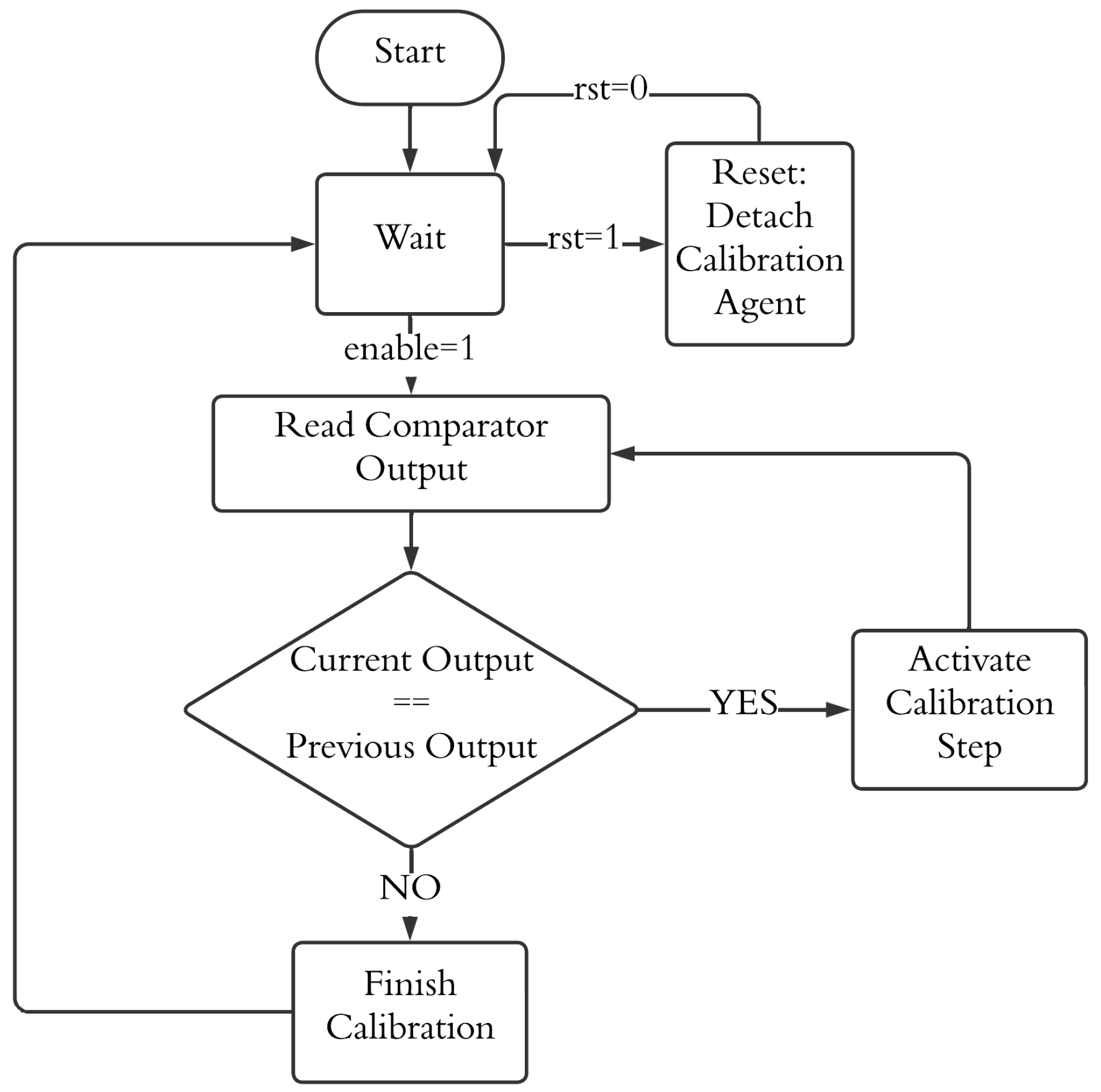
2.3. Calibration Algorithm
2.4. Other Calibration Circuitry/Techniques
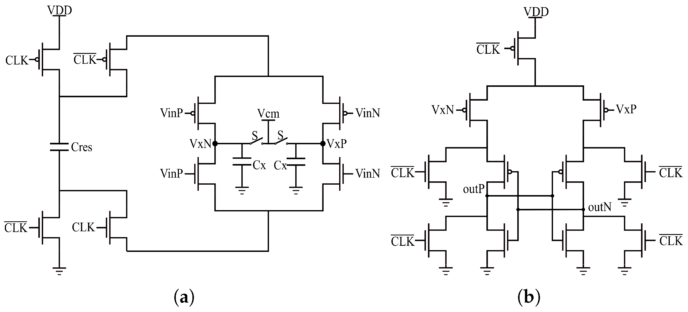
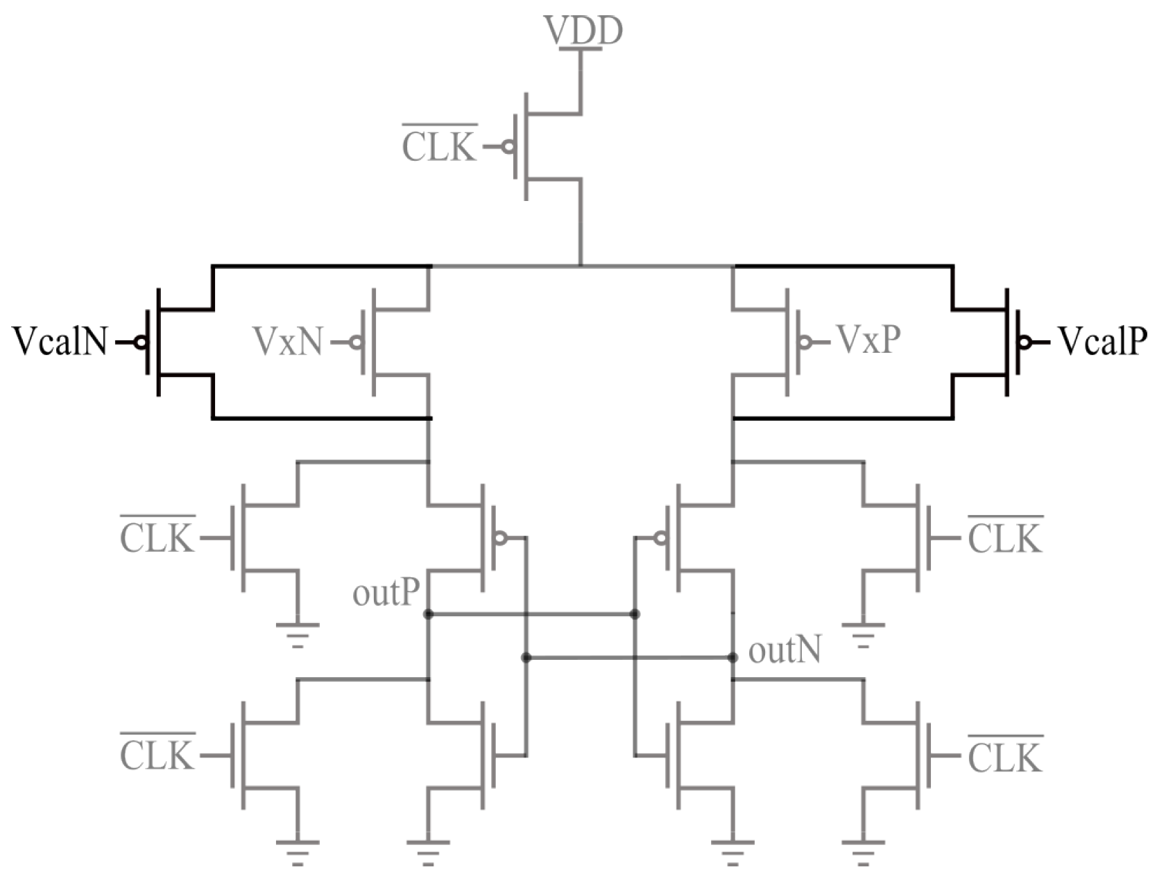
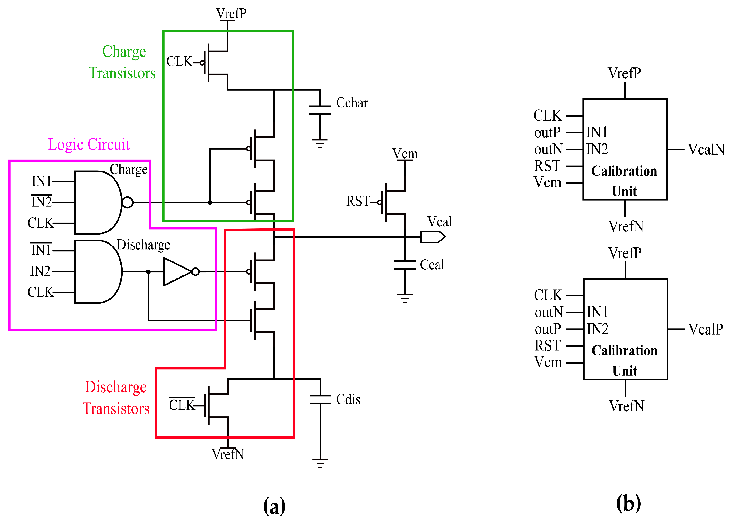
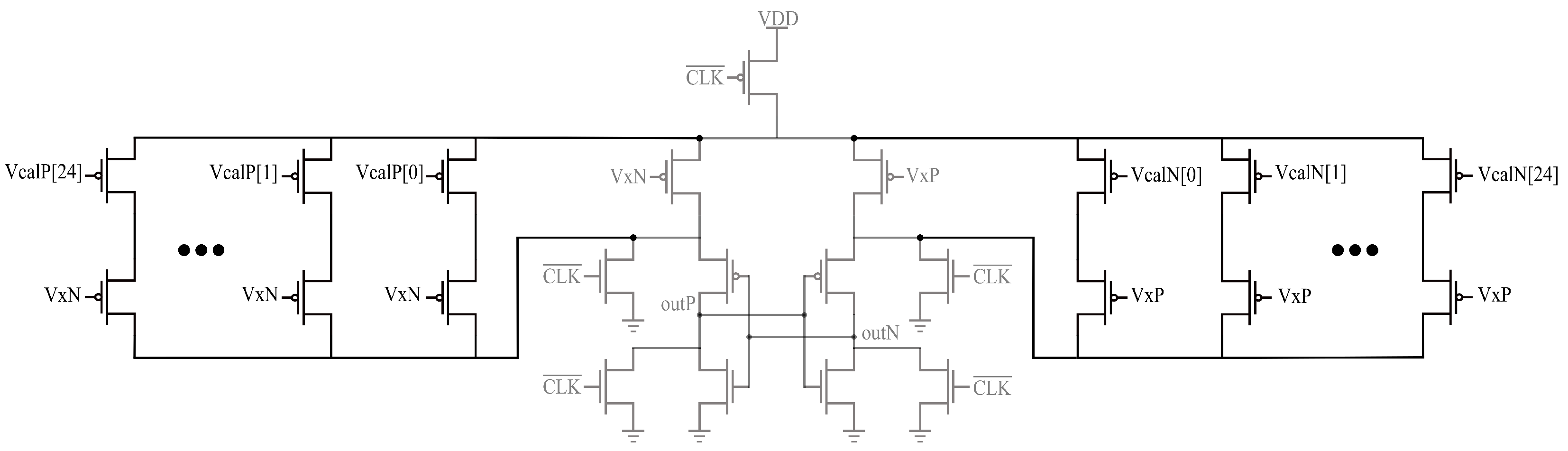
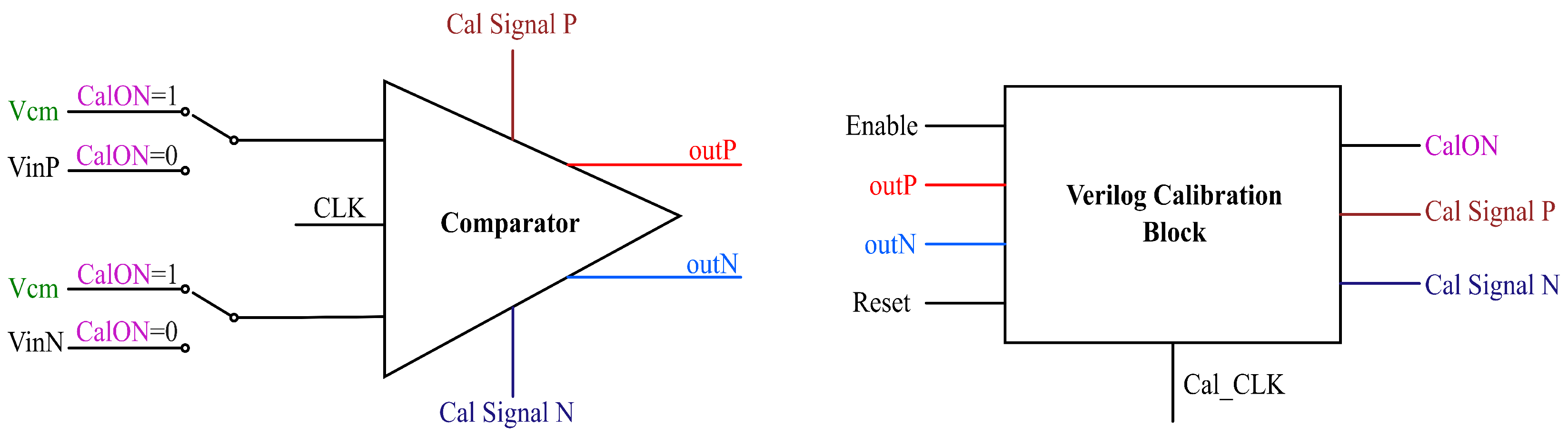
3. Proposed Offset Calibration Technique
3.1. Offset Compensation Circuitry
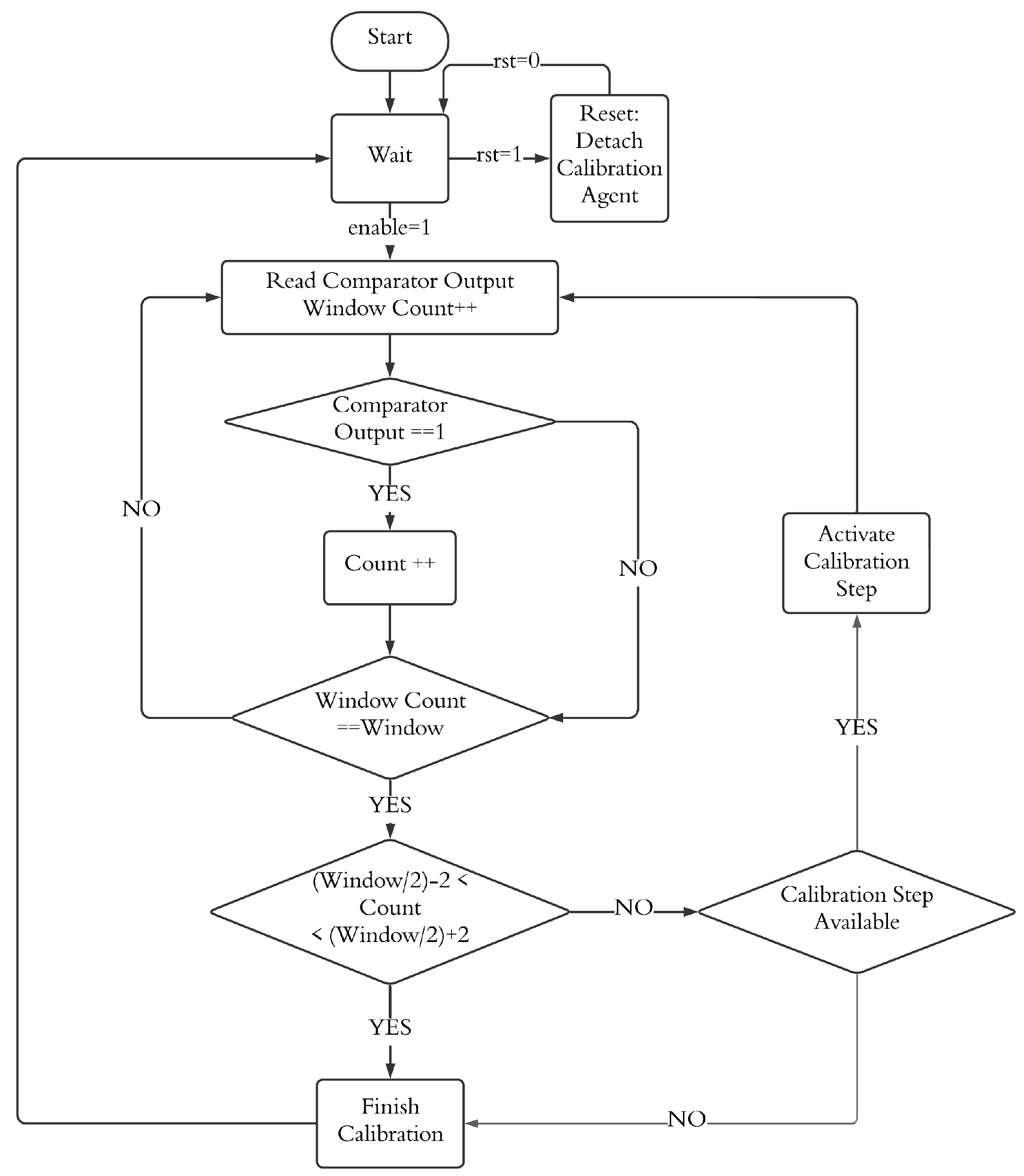
3.2. Window-Based Calibration Algorithm
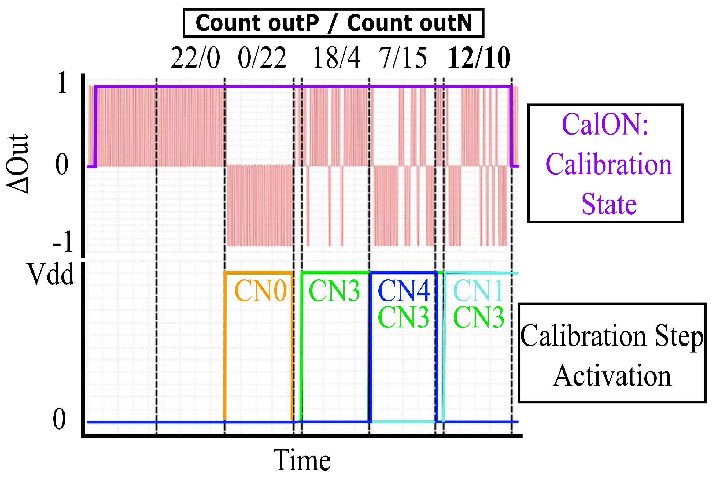
3.3. Functional Verification
4. Simulation Results
4.1. Offset Voltage and Input-Referred Noise Evaluation Methods
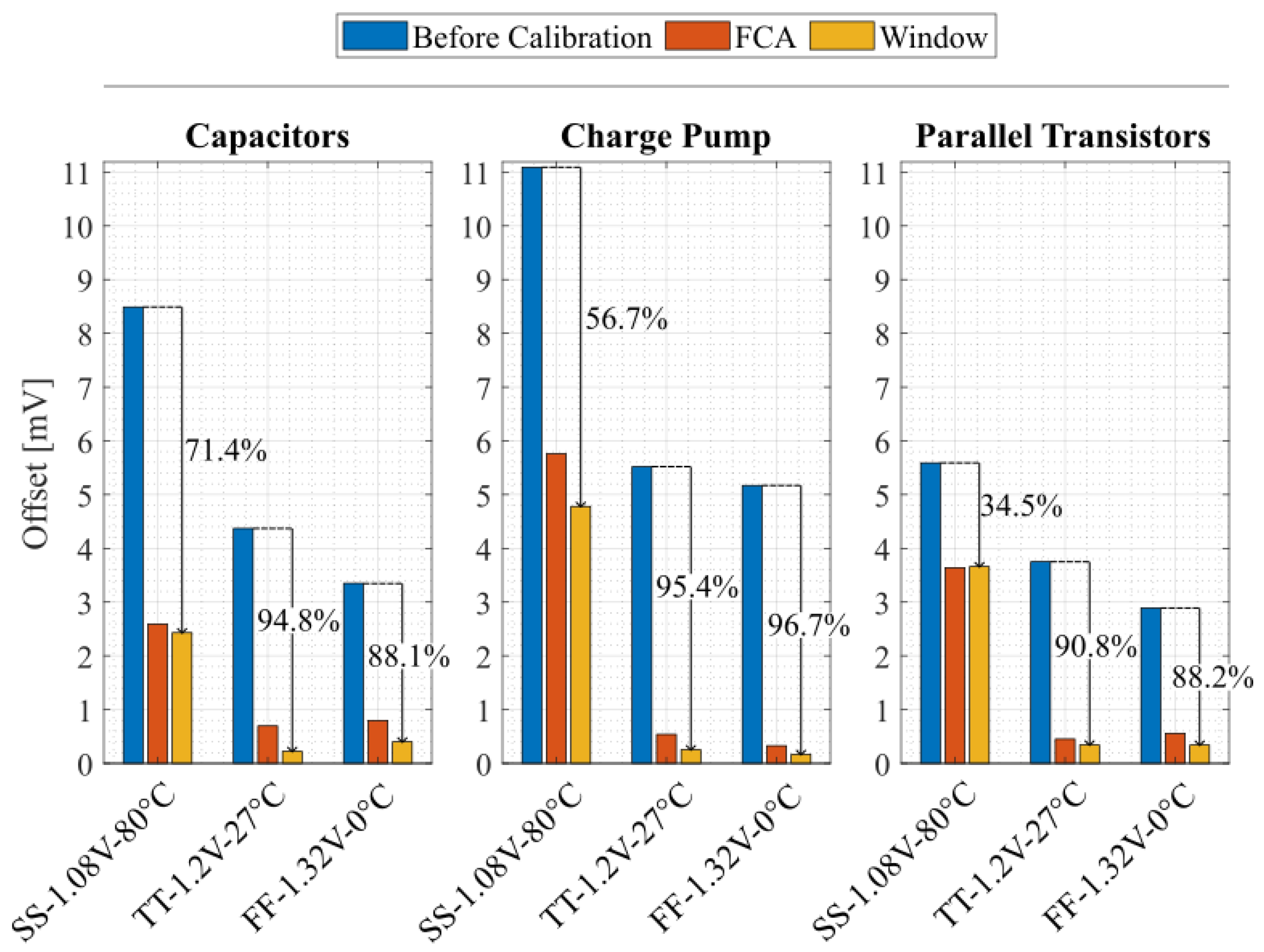
4.2. Offset Voltage Results
- Before calibration (Figure 12a,d,g,): A wide spread in offset values with high standard deviations demonstrates the inherent mismatch in the comparator design. Specifically, these results show that the comparator scheme with the parallel transistors array presents the lowest offset overall, while our proposal comes as second best. Finally, the charge pump method exhibits the highest initial offset.
- FCA (Figure 12b,e,h): The offset distribution becomes narrower, indicating that the offset values are less spread out. The lowest of 0.452 mV is observed in the parallel transistors approach, although this method also has the highest average offset. While this calibration method reduces the variation, some spread remains, as this solution relies on a single output toggle to determine the end of the calibration process, resulting in poor offset reduction accuracy. Moreover, there is a significant mean value in the offset after calibration for our proposed capacitor array.
- Proposed window-based calibration (Figure 12c,f,i): The smallest offset distributions, with both lower mean and standard deviation values. This indicates that window-based calibration effectively minimizes offset variation, producing values even lower than the input-referred noise as reported below in Table 3. Our proposed capacitor array and window algorithm solutions yielded the lowest offset-compensated value with a standard deviation of 0.2253 mV, followed by the charge pump circuit with a value of 0.2544 mV, and finally, the parallel transistors approach exhibited 0.3431 mV of compensated offset. For applications requiring precise offset control, window calibration is the preferred approach where the calibration time is not critical.
4.3. Performance Metrics

| Compensation Technique | Capacitive Load (Proposed) | Current Injection (Charge Pump) | Current Injection (Parallel Transistors) | |||
|---|---|---|---|---|---|---|
| Process [nm] | 65 | 65 | 65 | |||
| Supply Voltage [V] | 1.2 | 1.2 | 1.2 | |||
| Initial Offset Voltage [mV] | 4.37 | 5.52 | 3.75 | |||
| Fast (FCA) | Window (proposed) | Fast (FCA) | Window (proposed) | Fast (FCA) | Window (proposed) | |
| Calibrated Offset Voltage [mV] | = 0.183 = 0.696 | = 0.091 = 0.223 | = −0.025 = 0.539 | = 0.014 = 0.254 | = −0.254 = 0.452 | = −0.005 = 0.343 |
| Calibration Cycles | = 9 = 3 | = 166 = 42 | = 15 = 10 | = 310 = 217 | = 10 = 5 | = 156 = 42 |
| Average Energy per calibration cycle [pJ] | 0.175 | 0.165 | 0.233 | 0.202 | 0.217 | 0.216 |
|
Energy per comparison [pJ] Before calibration | 0.1474 @1 mV 0.1469 @10 mV | 0.131 @1 mV 0.130 @10 mV | 0.172 @1 mV 0.167 @10 mV | |||
|
Delay [ns] Before calibration | 4.09 @1 mV 3.44 @10 mV | 3.39 @1 mV 3.22 @10 mV | 7.36 @1 mV 5.49 @10 mV | |||
|
EDP [pJ·ns] Before calibration | 0.60 @1 mV 0.51 @10 mV | 0.44 @1 mV 0.42 @10 mV | 1.27 @1 mV 0.92 @10 mV | |||
| Noise [V] | 364.6 | 359.8 | 361.1 | |||
| Before calibration | ||||||
|
Energy per comparison [pJ] After calibration | 0.165 @1 mV 0.164 @10 mV | 0.207 @1 mV 0.192 @10 mV | 0.211 @1 mV 0.209 @10 mV | |||
|
Delay [ns] After calibration | 6.78 @1 mV 4.03 @10 mV | 2.69 @1 mV 1.84 @10 mV | 6.94 @1 mV 4.29 @10 mV | |||
|
EDP [pJ·ns] After calibration | 1.12 @1 mV 0.66 @10 mV | 0.56 @1 mV 0.35 @10 mV | 1.46 @1 mV 0.89 @10 mV | |||
| Noise [V] | 365.3 | 392.4 | 345.8 | |||
| After calibration | ||||||
| fmax [MHz] (3-) | 30.23 @1 mV 63.73 @10 mV | 78.60 @1 mV 122.30 @10 mV | 4.97 @1 mV 29.54 @10 mV | |||
| Area [m2] | Transistors: 65 MIMCaps: 10.6 | Transistors: 39 MIMcaps: 1266 | 122 | |||
- Calibration cycles: The number of cycles required to complete calibration varies significantly. Using the FCA, the capacitive and parallel transistor techniques present the lowest cycle counts (9 and 10 cycles, respectively), followed by the charge pump method (15 cycles). However, the window-based algorithm presents a higher and variable cycle count due to its iterative process, required to minimize the offset. Capacitive and parallel transistor techniques complete calibration in 166 and 156 cycles, respectively, while the charge pump method requires 310 cycles, nearly double the others.
- Average calibration energy: The proposed capacitive load technique is the most energy efficient, requiring an average energy per calibration cycle of 0.175 pJ for fast calibration and 0.165 pJ for window-based calibration. The charge pump technique is the least efficient, consuming 0.233 pJ/cycle and 0.202 pJ/cycle for fast and window calibration, respectively. The parallel transistor method lies in between, with 0.217 pJ/cycle for fast calibration and 0.216 pJ/cycle for the window-based algorithm. Note that the proposed window-based approach requires a higher number of calibration cycles compared to the FCA-based compensation techniques. Therefore, the overall energy consumed during the entire calibration process is higher.
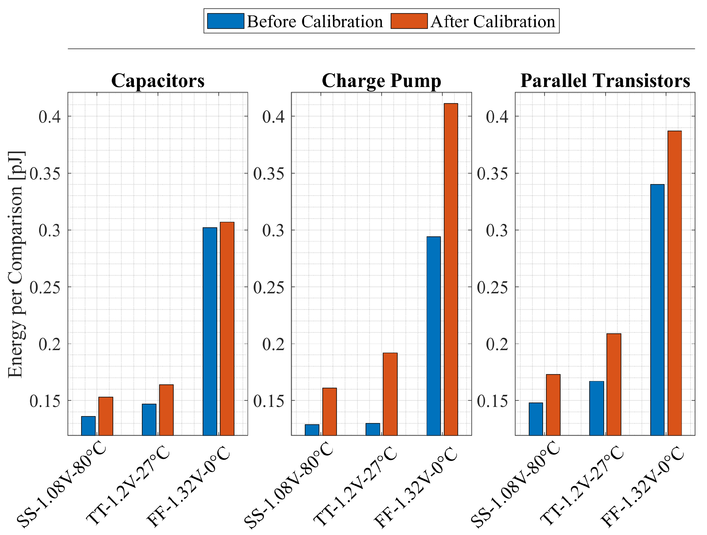
- Energy per comparison and delay (refer to highlighted results in Table 3): Energy values with no calibration applied are lowest for the charge pump technique (0.131 pJ at = 1 mV), followed by the capacitive load technique (0.147 pJ at = 1 mV) and the parallel transistors technique consuming the most energy (0.172 pJ at = 1 mV). After calibration, energy consumption increases for all methods, with the current injection methods consuming more energy than the capacitive load technique. In terms of delay, the charge pump technique achieves the lowest delay, showing a delay of 3.39 ns and 2.69 ns at = 1 mV, with and without calibration, respectively. Our proposed solution achieves a post-calibration delay of 6.78 ns, compared to 4.09 ns with no calibration applied. On the other hand, the parallel transistors technique has the highest delay after calibration (6.94 ns at = 1 mV). Using either the charge pump or parallel transistors approaches results in a delay performance increase compared to the operation with no offset compensation. This improvement is a consequence of the nature of these methodologies, which involve a current injection that increases the drive strength of the output latch.
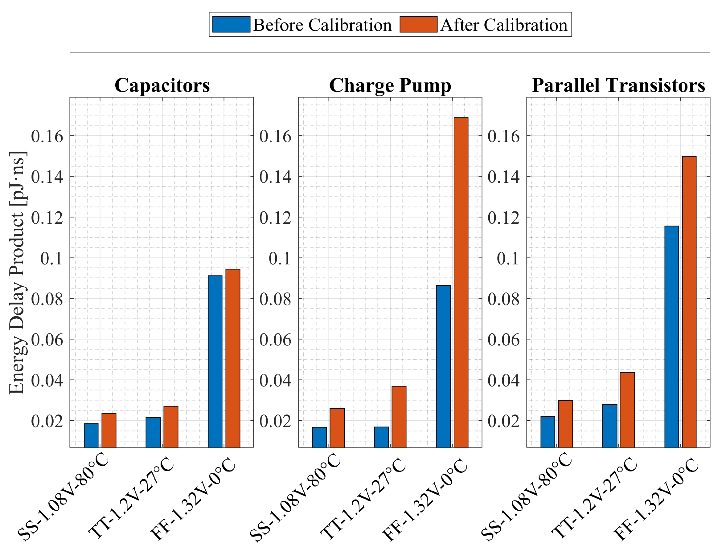
- Energy-Delay Product, EDP (refer to highlighted results in Table 3): The charge pump technique achieves the lowest EDP at = 1 mV, with calibration (0.56 pJ·ns) and without calibration (0.44 pJ·ns), indicating high efficiency. The capacitive load technique also achieves a relatively low EDP without calibration (0.60 pJ·ns at = 1 mV); however, after calibration, its EDP increases due to the longer delay, although it improves (decreases) as increases. In contrast, the parallel transistors approach has the highest EDP, making it less efficient when balancing energy consumption and speed.
- Power consumption: Power consumption is evaluated with a clock period of 200 and a = 1 mV. Prior calibration, the obtained average power consumption per comparison by employing the parallel transistors technique is 0.860 W, the capacitive load method follows with a consumption of 0.737 W, while the charge pump approach consumes 0.655 W. After calibration, the obtained power consumption is 1.055 W for the parallel transistors, 1.035 W for the charge pump method, and 0.825 W for the capacitive load method, which remains the most power efficient technique.
- Noise performance (refer to highlighted results in Table 3): Prior to calibration, all techniques present similar levels of noise. However, the impact of calibration on noise varies across methods. The capacitive load presents an slight increase ab about 1 V. The parallel transistors approach achieves a reduction of 15 V in noise. As for the charge pump technique, it presents the most significant noise degradation, with an increase of 32 V, which may be a concern for noise-sensitive designs
- Maximum operating frequency: The maximum frequency is calculated as the inverse of twice the propagation delay, obtained under 1000 Monte Carlo samples, and reported at 3- in Table 3. The charge pump method presents the highest operation frequency (122.3 MHz at = 10 mV), making it the most suitable for high-speed applications. The proposed capacitive load approach operates at a maximum frequency of 63.73 MHz at = 10 mV. The parallel transistors method presents the lowest maximum frequency (29.54 MHz), which is a trade-off to achieve an accurate calibration of the offset voltage as it needs more transistors to provide a smaller calibration step at the expense of longer delay.
- Area overhead: The charge pump method presents and area-footprint of about 1305 m2, from which 1266 m2 is due to the MIM capacitors. The proposed capacitive load method occupies a total area footprint of about 75.6 m2, the lowest among the other calibration techniques.
4.4. Process, Voltage, and Temperature Variation Analysis
4.5. Summary
5. Conclusions
Author Contributions
Funding
Data Availability Statement
Conflicts of Interest
References
- Hershberg, B.; Dermit, D.; van Liempd, B.; Martens, E.; Markulić, N.; Lagos, J.; Craninckx, J. A 4-GS/s 10-ENOB 75-mW Ringamp ADC in 16-nm CMOS With Background Monitoring of Distortion. IEEE J.-Solid-State Circuits 2021, 56, 2360–2374. [Google Scholar] [CrossRef]
- Goll, B.; Zimmermann, H. Comparators in Nanometer CMOS Technology; Springer: Berlin/Heidelberg, Germany, 2015; Volume 50, p. 250. [Google Scholar] [CrossRef]
- Hung, W.P.; Chang, C.H.; Lee, T.H. Real-Time and Noncontact Impulse Radio Radar System for μm Movement Accuracy and Vital-Sign Monitoring Applications. IEEE Sens. J. 2017, 17, 2349–2358. [Google Scholar] [CrossRef]
- Sakr, A.; Hussein, A.I.; Fahmy, G.A.; Abdelghany, M.A. High-Speed Comparator Design for RF-to-Digital Receivers. In Proceedings of the 2020 37th National Radio Science Conference (NRSC), Cairo, Egypt, 8–10 September 2020; pp. 207–215. [Google Scholar] [CrossRef]
- Fan, H.; Li, J.; Maloberti, F. Order statistics and optimal selection of unit elements in DACs to enhance the static linearity. IEEE Trans. Circuits Syst. I Regul. Pap. 2020, 67, 2193–2203. [Google Scholar] [CrossRef]
- Gagliardi, F.; Scintu, D.; Piotto, M.; Bruschi, P.; Dei, M. Static-Linearity Enhancement Techniques for Digital-to-Analog Converters Exploiting Optimal Arrangements of Unit Elements. IEEE Trans. Very Large Scale Integr. (VLSI) Syst. 2024, 32, 2243–2256. [Google Scholar] [CrossRef]
- Renteria-Pinon, M.; Tang, X.; Tang, W. Real-Time In-Sensor Slope Level-Crossing Sampling for Key Sampling Points Selection for Wearable and IoT Devices. IEEE Sens. J. 2023, 23, 6233–6242. [Google Scholar] [CrossRef]
- Zhao, X.; Li, D.; Zhang, X.; Liu, S.; Zhu, Z. A 0.6-V 94-nW 10-Bit 200-kS/s Single-Ended SAR ADC for Implantable Biosensor Applications. IEEE Sens. J. 2022, 22, 17904–17913. [Google Scholar] [CrossRef]
- Shifman, Y.; Shor, J. An 11 uW, 0.08 mm2, 125 dB-Dynamic-Range Current-Sensing Dynamic CT Zoom ADC. IEEE Trans. Circuits Syst. I: Regul. Pap. 2024, 71, 3489–3501. [Google Scholar] [CrossRef]
- Chen, P.; Zhao, W.; Wu, M.; Shen, L.; Jia, T.; Huang, R.; Ye, L.; Ma, Y. A 22-nm Delta–Sigma Computing-In-Memory SRAM Macro With Near-Zero-Mean Outputs and LSB-First ADCs for Edge AI Processing. IEEE J.-Solid-State Circuits 2025. [Google Scholar] [CrossRef]
- Tagata, H.; Sato, T.; Awano, H. Double MAC on a Cell: A 22-nm 8T-SRAM Based Analog In-Memory Accelerator for Binary/Ternary Neural Networks Featuring Split Wordline. IEEE Open J. Circuits Syst. 2024, 5, 328–340. [Google Scholar] [CrossRef]
- Li, T.; Huang, J.; Zeng, J.; Guo, C.; Zhang, W.; Fu, X.; Xu, D.; Yan, G.; Jiang, J.; Lai, R.; et al. A digital background calibration method for SAR ADC based on dual-layer feedforward neural network. Microelectron. J. 2025, 159, 106645. [Google Scholar] [CrossRef]
- Kim, S.; Kim, S.; Um, S.; Kim, S.; Kim, K.; Yoo, H.J. Neuro-CIM: ADC-Less Neuromorphic Computing-in-Memory Processor With Operation Gating/Stopping and Digital–Analog Networks. IEEE J.-Solid-State Circuits 2023, 58, 2931–2945. [Google Scholar] [CrossRef]
- Rafiq, M.; Chatterjee, S.; Kumar, S.; Singh Chauhan, Y.; Sahay, S. Utilizing Dual-Port FeFETs for Energy-Efficient Binary Neural Network Inference Accelerators. IEEE Trans. Electron Devices 2024, 71, 4381–4388. [Google Scholar] [CrossRef]
- Qi, X.; Zhao, J.; Lou, Y.; Wang, G.; Tang, K.T.; Li, Y. A 5.3 pJ/Spike CMOS Neural Array Employing Time-Modulated Axon-Sharing and Background Mismatch Calibration Techniques. IEEE Trans. Biomed. Circuits Syst. 2023, 17, 286–298. [Google Scholar] [CrossRef]
- Sangeetha, R.; Vidhyashri, A.; Reena, M.; Sudharshan, R.B.; govindan, S.; Ajayan, J. An Overview Of Dynamic CMOS Comparators. In Proceedings of the 2019 5th International Conference on Advanced Computing Communication Systems (ICACCS), Coimbatore, India, 15–16 March 2019; pp. 1001–1004. [Google Scholar] [CrossRef]
- Tang, X.; Shen, L.; Kasap, B.; Yang, X.; Shi, W.; Mukherjee, A.; Pan, D.Z.; Sun, N. An Energy-Efficient Comparator With Dynamic Floating Inverter Amplifier. IEEE J.-Solid-State Circuits 2020, 55, 1011–1022. [Google Scholar] [CrossRef]
- Razavi, B. The StrongARM latch [A Circuit for All Seasons]. IEEE Solid-State Circuits Mag. 2015, 7, 12–17. [Google Scholar] [CrossRef]
- Tsirmpas, G.; Kontelis, S.; Souliotis, G.; Plessas, F. A high-speed dynamic comparator with automatic offset calibration. AEU-Int. J. Electron. Commun. 2024, 186, 155472. [Google Scholar] [CrossRef]
- Jaiswal, S.K.; Mondal, A.; Srimani, S.; Das, S.; Ghosh, K.; Rahaman, H. Design of a low power, high speed self calibrated dynamic latched comparator. In Proceedings of the 2020 International Symposium on Devices, Circuits and Systems (ISDCS), Howrah, India, 4–6 March 2020; pp. 1–6. [Google Scholar] [CrossRef]
- Lee, J.; Lim, Y.; Sung, B.; Oh, S.; Chun, J.H.; Lee, J. An Effective Transconductance Controlled Offset Calibration for Dynamic Comparators. In Proceedings of the 2020 IEEE International Symposium on Circuits and Systems (ISCAS), Virtual Conference, 14–21 October 2020; pp. 1–5. [Google Scholar] [CrossRef]
- Sharma, N.; Srivastava, R.K.; Hande, V.; Sehgal, D.; Das, D.M. A Self-Calibration Logic Circuit Agnostic To Offset Calibration Technique For High-Precision Dynamic Comparator. In Proceedings of the 2023 IEEE Women in Technology Conference (WINTECHCON), Bangalore, India, 21 September 2023; pp. 1–6. [Google Scholar] [CrossRef]
- Ahrar, A.; Yavari, M. A Digital Method for Offset Cancellation of Fully Dynamic Latched Comparators. In Proceedings of the 2021 29th Iranian Conference on Electrical Engineering (ICEE), Tehran, Iran, 18–20 May 2021; pp. 143–148. [Google Scholar] [CrossRef]
- Yousefirad, M.; Yavari, M. Kick-back Noise Reduction and Offset Cancellation Technique for Dynamic Latch Comparator. In Proceedings of the 2021 29th Iranian Conference on Electrical Engineering (ICEE), Tehran, Iran, 18–20 May 2021; pp. 149–153. [Google Scholar] [CrossRef]
- Nuzzo, P.; De Bernardinis, F.; Terreni, P.; Van der Plas, G. Noise analysis of regenerative comparators for reconfigurable ADC architectures. IEEE Trans. Circuits Syst. I Regul. Pap. 2008, 55, 1441–1454. [Google Scholar] [CrossRef]
- Van der Plas, G.; Decoutere, S.; Donnay, S. A 0.16 pJ/conversion-step 2.5 mW 1.25 GS/s 4b ADC in a 90 nm digital CMOS process. In Proceedings of the 2006 IEEE International Solid State Circuits Conference-Digest of Technical Papers, San Francisco, CA, USA, 6–9 February 2006; p. 2310. [Google Scholar]
- Li, D.; Meng, Q.; Li, F.; Wang, L. An analysis of offset calibration based additional load capacitor imbalance for two-stage dynamic comparator. In Proceedings of the 2016 6th International Conference on Information Communication and Management (ICICM), Hatfield, UK, 29–31 October 2016; pp. 264–267. [Google Scholar]
- Zlochisti, M.; Zahrai, S.A.; Onabajo, M. Digitally programmable offset compensation of comparators in flash ADCs for hybrid ADC architectures. In Proceedings of the 2015 IEEE 58th International Midwest Symposium on Circuits and Systems (MWSCAS), Fort Collins, CO, USA, 2–5 August 2015; pp. 1–4. [Google Scholar]
- Figueiredo, P.M.; Cardoso, P.; Lopes, A.; Fachada, C.; Hamanishi, N.; Tanabe, K.; Vital, J. A 90 nm CMOS 1.2 v 6b 1GS/s two-step subranging ADC. In Proceedings of the 2006 IEEE International Solid State Circuits Conference-Digest of Technical Papers, San Francisco, CA, USA, 5–9 February 2006; pp. 2320–2329. [Google Scholar]
- Castaldo, E.; Gibilaro, M.E. A Comprehensive Analog–Mixed Signal (AMS) Simulations Environment. Chips 2024, 3, 258–270. [Google Scholar] [CrossRef]
- Graupner, A.; Sobe, U. Offset-Simulation of Comparators. Core—An Open Scholarly Infrastructure for Researchers 2007. Available online: https://nbn-resolving.org/urn:nbn:de:swb:ch1-200700897 (accessed on 30 October 2024).
- Chevella, S.; O’Hare, D.; O’Connell, I. A low-power 1-V supply dynamic comparator. IEEE Solid-State Circuits Lett. 2020, 3, 154–157. [Google Scholar] [CrossRef]
- Satpathy, B.; Srivastava, U.; Kaur, A. An Asymmetric Dynamic Comparator for Low Offset, Low Noise and High Speed Applications. IEEE Trans. Instrum. Meas. 2025, 55, 2003508. [Google Scholar] [CrossRef]
- Pan, F.; Pham, T. Capacitive Regulation of Charge Pumps Without Refresh Operation interruption. US Patent 9,077,238, 7 July 2015. [Google Scholar]
- Ballo, A.; Grasso, A.D.; Palumbo, G. A memory-targeted dynamic reconfigurable charge pump to achieve a power consumption reduction in IoT nodes. IEEE Access 2021, 9, 41958–41964. [Google Scholar] [CrossRef]


| Units | [19] | [20] | [21] | [22] | [23] | [24] | |
|---|---|---|---|---|---|---|---|
| Process Node | nm | 65 | 180 | 14 | 180 | 180 | 180 |
| Supply Voltage | V | 1 | 1.8 | 0.9 | 1.8 | 1 | 1.1 |
| Calibration Technique | – | Discharge Current | Discharge Current | Discharge Current | Discharge Current | Discharge Current- Body Bias | Body Bias |
| Initial Offset | mV | 16 | 2.72 | 2.073 | 2.85 | 19.56 | 13.2 |
| Calibrated Offset | mV | 1 | 0.013 | 0.259 | 0.445 | 0.363 | 0.3 |
| Energy/Comparison * | pJ | - | 0.134 | 0.214 | 0.155 | 0.952–10.66 | 0.036 |
| Capacitor | Size | Offset Compensation |
|---|---|---|
| C0 (MIM-Cap) | 2.3 m × 2.3 m | ∼5 mV |
| C1 | 120 nm × 60 nm | ∼0.5 mV |
| C2 | 120 nm × 60 nm | ∼0.5 mV |
| C3 | 240 nm × 240 nm | ∼1 mV |
| C4 | 290 nm × 280 nm | ∼1 mV |
| C5 | 350 nm × 350 nm | ∼1 mV |
| C6 | 440 nm × 400 nm | ∼1 mV |
| C7 | 600 nm × 600 nm | ∼1 mV * |
| C8 | 750 nm × 750 nm | ∼1 mV * |
| C9 | 950 nm × 950 nm | ∼1 mV * |
| C10 | 1.7 m × 850 nm | ∼1 mV * |
Disclaimer/Publisher’s Note: The statements, opinions and data contained in all publications are solely those of the individual author(s) and contributor(s) and not of MDPI and/or the editor(s). MDPI and/or the editor(s) disclaim responsibility for any injury to people or property resulting from any ideas, methods, instructions or products referred to in the content. |
© 2025 by the authors. Licensee MDPI, Basel, Switzerland. This article is an open access article distributed under the terms and conditions of the Creative Commons Attribution (CC BY) license (https://creativecommons.org/licenses/by/4.0/).
Share and Cite
Cuenca, J.; Zambrano, B.; Garzón, E.; Prócel, L.M.; Lanuzza, M. An Accurate and Low-Complexity Offset Calibration Methodology for Dynamic Comparators. J. Low Power Electron. Appl. 2025, 15, 35. https://doi.org/10.3390/jlpea15020035
Cuenca J, Zambrano B, Garzón E, Prócel LM, Lanuzza M. An Accurate and Low-Complexity Offset Calibration Methodology for Dynamic Comparators. Journal of Low Power Electronics and Applications. 2025; 15(2):35. https://doi.org/10.3390/jlpea15020035
Chicago/Turabian StyleCuenca, Juan, Benjamin Zambrano, Esteban Garzón, Luis Miguel Prócel, and Marco Lanuzza. 2025. "An Accurate and Low-Complexity Offset Calibration Methodology for Dynamic Comparators" Journal of Low Power Electronics and Applications 15, no. 2: 35. https://doi.org/10.3390/jlpea15020035
APA StyleCuenca, J., Zambrano, B., Garzón, E., Prócel, L. M., & Lanuzza, M. (2025). An Accurate and Low-Complexity Offset Calibration Methodology for Dynamic Comparators. Journal of Low Power Electronics and Applications, 15(2), 35. https://doi.org/10.3390/jlpea15020035