Abstract
Dynamic comparators play an important role in electronic systems, requiring high accuracy, low power consumption, and minimal offset voltage. This work proposes an accurate and low-complexity offset calibration design based on a capacitive load approach. It was designed using a 65 nm CMOS technology and comprehensively evaluated under Monte Carlo simulations and PVT variations. The proposed scheme was built using MIM capacitors and transistor-based capacitors, and it includes Verilog-based calibration algorithms. The proposed offset calibration is benchmarked, in terms of precision, calibration time, energy consumption, delay, and area, against prior calibration techniques: current injection via gate biasing by a charge pump circuit and current injection via parallel transistors. The evaluation of the offset calibration schemes relies on Analog/Mixed-Signal (AMS) simulations, ensuring accurate evaluation of digital and analog domains. The charge pump method achieved the best Energy-Delay Product (EDP) at the cost of lower long-term accuracy, mainly because of its capacitor leakage. The proposed scheme demonstrated superior performance in offset reduction, achieving a one-sigma offset of 0.223 mV while maintaining precise calibration. Among the calibration algorithms, the window algorithm performs better than the accelerated calibration. This is mainly because the window algorithm considers noise-induced output oscillations, ensuring consistent calibration across all designs. This work provides insights into the trade-offs between energy, precision, and area in dynamic comparator designs, offering strategies to enhance offset calibration.
1. Introduction
Comparators are essential circuit blocks in modern electronic systems, serving as high-speed decision-making components in applications that require fast and accurate signal evaluation. Their role is particularly valuable in analog-to-digital converters (ADCs) [1], where they determine the digital representation of input signals, directly influencing system performance [2]. Beyond ADCs, comparators are widely used in Ultra-Wideband (UWB) communication systems [3] to decode received signals and in Software-Defined Radio (SDR) systems [4], where they enable flexible system reconfiguration by placing ADCs and digital-to-analog converters (DACs) closer to the antenna. Dynamic comparators are also integral to recent DAC calibration schemes that use optimal reordering of unit-element switching sequences to improve static linearity [5,6]. In the context of the Internet of Things (IoT) [7], comparators assist real-time quantization in sensor nodes and wearable devices, selecting sampling points and verifying input thresholds. Furthermore, they play a crucial role in biomedical applications, such as implantable biosensors [8,9], where low-offset, low-noise comparators enable precise signal conversion in Successive Approximation Register (SAR) ADCs. Furthermore, dynamic comparators as well as calibration schemes have gained interest in deep learning architectures [10,11,12] and neuromorphic computing architectures [13,14,15]. As for the latter, 1-bit dynamic comparators are employed as a low-overhead alternative to conventional ADCs within Spiking Neural Networks (SNNs), enabling highly efficient signal quantization while significantly minimizing power consumption and silicon footprint [13,14,15].
Despite their widespread use, the design of CMOS dynamic comparators faces several critical challenges, such as ensuring high-speed operation while minimizing power consumption and maintaining minimal offset voltage without compromising reliability [16]. Among these challenges, offset voltage, defined as the minimum differential input voltage required to toggle the output, remains a critical issue as it directly affects comparator accuracy. Ideally, the offset voltage should be zero; however, it deviates due to inherent transistor mismatches introduced during the fabrication process as well as asymmetries in layout design. These variations can shift the comparator switching threshold, leading to incorrect decision-making in applications that require precise signal detection. Although careful layout techniques can mitigate mismatch-induced offsets to some extent, circuit-level calibration is often required to achieve accurate and reliable offset compensation.
This work presents an accurate and low-complexity offset calibration methodology based on a capacitive load tuning approach. A comprehensive comparative analysis of existing offset calibration techniques is first presented, followed by a discussion of a novel automatic calibration strategy specifically designed to efficiently mitigate offset variations. The proposed methodology builds on the two-stage dynamic comparator design introduced in [17] by adapting two existing calibration techniques to the same comparator structure to ensure fair comparison. The proposed approach, as well as the baseline comparison, was designed using a 65 nm commercial process and evaluated under extensive Monte Carlo simulations while taking into account layout parasitics and process–voltage–temperature variations.
The remainder of the paper is organized as follows: Section 2 reviews existing calibration techniques and the standard algorithms employed in prior works. Section 3 details the proposed calibration method, which leverages noise fluctuations as a measure of a successful calibration. Section 4 presents comprehensive simulation results, comparing the proposed approach with existing techniques in terms of offset reduction capabilities and performance trade-offs. Section 5 summarizes the key findings of this work.
2. Background: Calibration Techniques and Algorithm
The mismatch in comparator circuits predominantly affects transistors that are activated during the initial phase of the comparison process as their early switching has a more pronounced influence on the offset [18]. To mitigate this, a variety of offset reduction techniques have been developed, broadly categorized into static and dynamic offset cancellation methods. Static offset cancellation involves the integration of additional components, such as transistors or capacitors, to balance the load or current on the mismatched side. On the other side, dynamic offset cancellation introduces an extra stage preceding the comparator, which senses and corrects the offset, thereby preventing it from propagating to the latch stage. Nevertheless, the latch itself can also contribute to the offset, which means that combining static and dynamic techniques within the same comparator can lead to more effective offset mitigation [2].
Several previous studies have proposed techniques to mitigate offset in comparators [19,20,21,22,23]. In [19,21,22,23], parallel transistors are sequentially activated based on the measured offset magnitude. In [20], a charge pump is used to provide voltage to two additional transistors to increase or decrease current in specific branches. In [23,24], body bias control is applied to the differential input of the comparator, adjusting their threshold voltage () according to the measured offset. These methods rely on sensing the comparator outputs to determine the offset direction and magnitude. Consequently, digital control blocks are used to implement effective calibration. This calibration process typically involves activating and tuning specific circuit elements until the offset is minimized.
Table 1 summarizes the mentioned calibration techniques, detailing their pre-calibration and post-calibration offsets along with the associated energy consumption.

Table 1.
State-of-the-art offset calibration techniques.
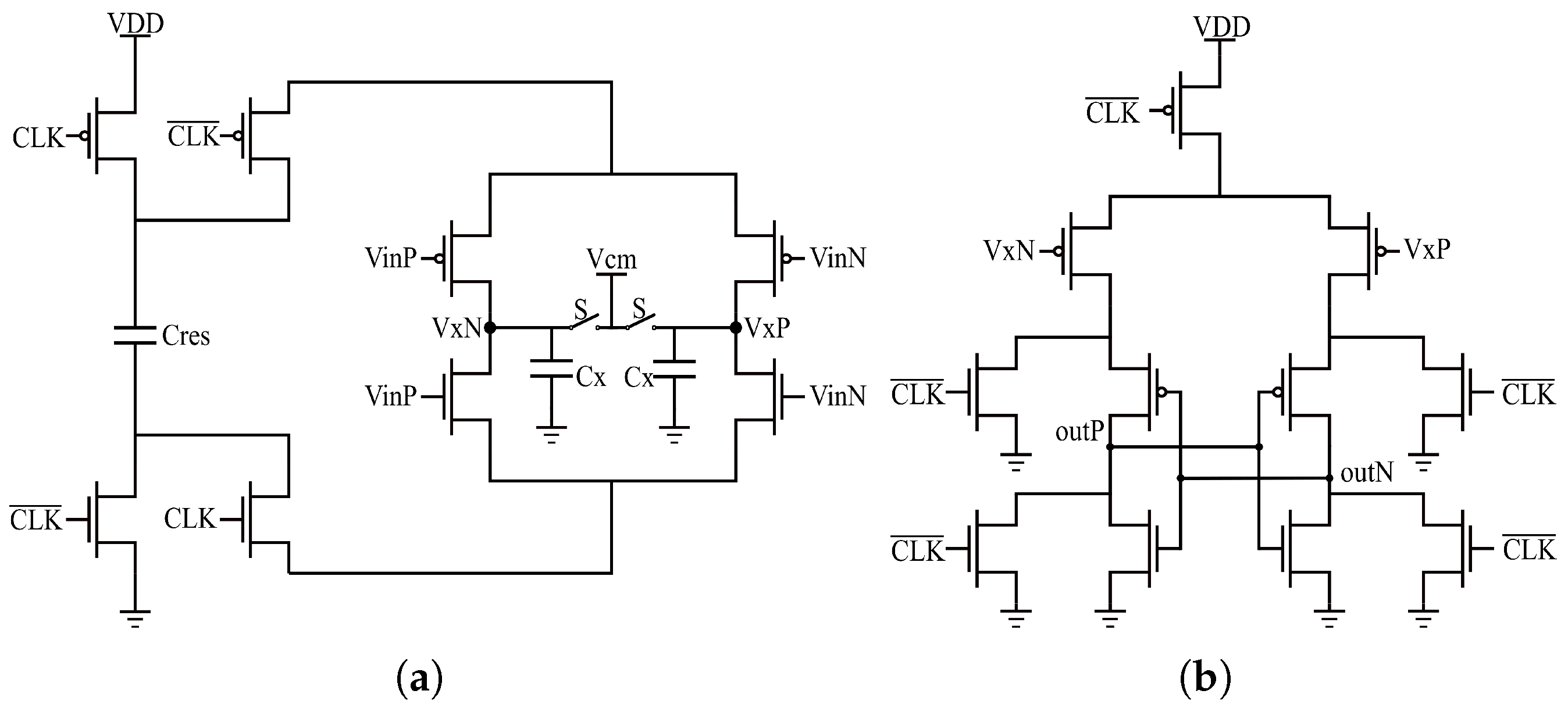
In this work, the dynamic comparator shown in Figure 1, based on the design in [17], is used as a baseline to implement and evaluate different offset calibration techniques. It consists of a Floating Inverter Amplifier (FIA) followed by a clocked latch. The FIA, illustrated in Figure 1a, processes the differential input signals (VinP and VinN), bringing them to a level suitable for reliable detection by the latch (Figure 1b), while improving performance, energy efficiency, and noise management through pre-amplification. The clocked latch then generates a digital output based on the amplified differential input.
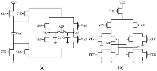
Figure 1.
Two-stage dynamic comparator [17]. (a) First stage: Floating inverter amplifier. (b) Second stage: Output latch.
Solutions presented in [20,21,22] were adapted into this dynamic comparator (refer to Figure 1). Their operational principles are detailed below, as they form the basis for the comparative evaluation presented later in Section 4.
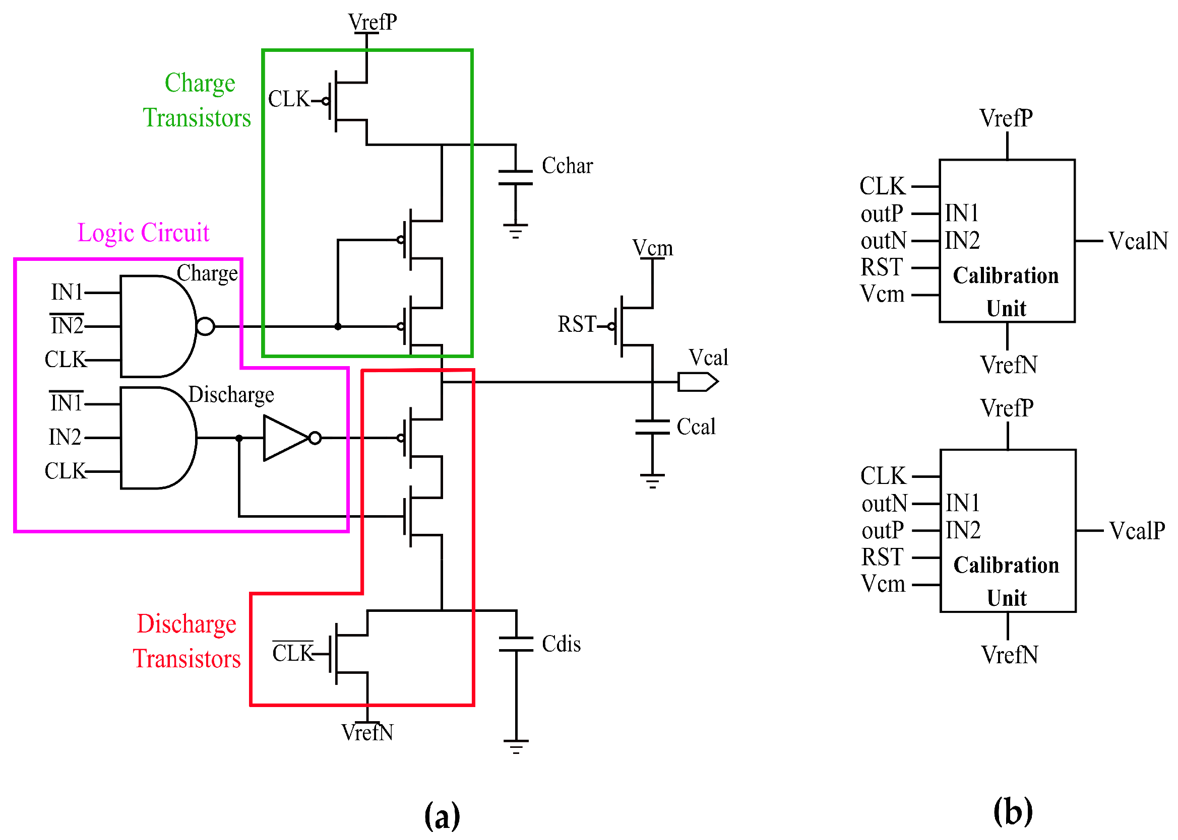
2.1. Calibration Technique: Current Injection via Gate Biasing by a Charge Pump Circuit
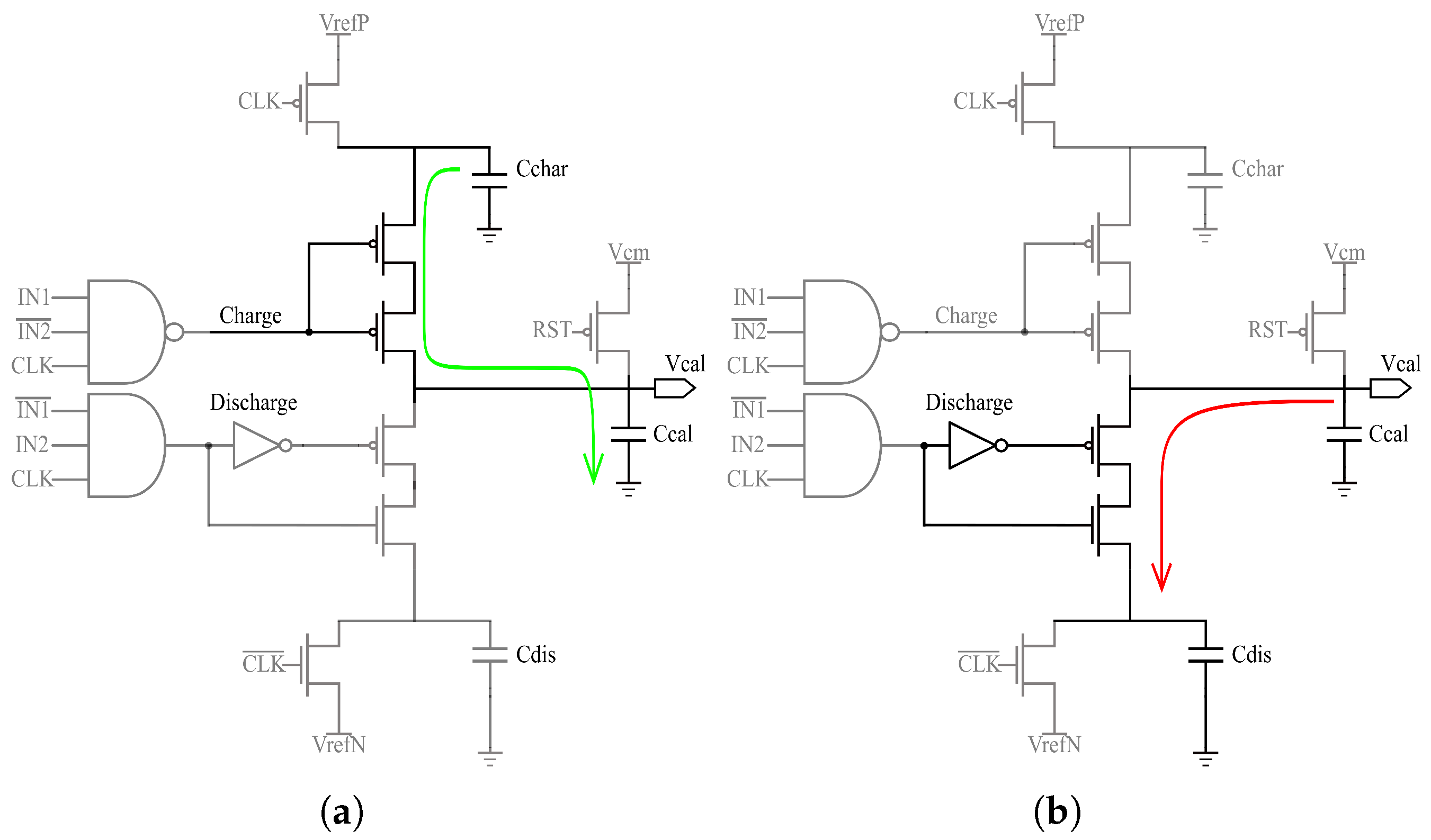
The method introduced in [20] employs a current injection approach using two additional transistors, each in parallel to the input transistors, as shown in Figure 2. The gate of these transistors is driven by the voltages VcalN and VcalP that are generated by the charge pump circuitry shown in Figure 3a. This circuitry regulates the injected current of the left and right branches of the output latch (refer to Figure 1b), counteracting the offset. This charge pump circuit is referred to as a calibration unit, and for a single comparator, two calibration units are required, as shown in Figure 3b.

Figure 2.
Additional transistors in the second stage (output latch) of the dynamic comparator for offset calibration.
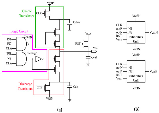
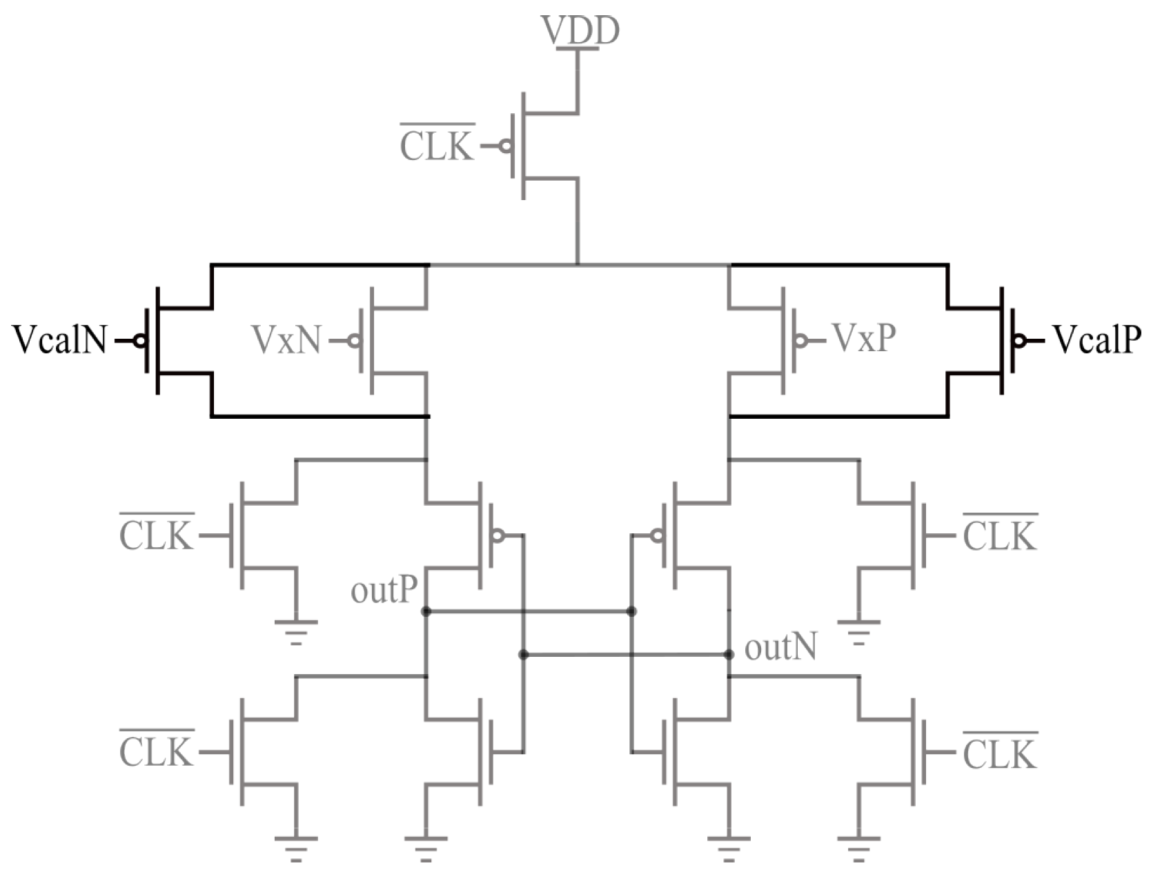
Figure 3.
Charge pump circuitry: (a) schematic, (b) top-level view of two (VcalN and VcalP) calibration units.
The charge pump in Figure 3a ensures precise calibration by selectively activating Charge and Discharge signals based on the comparator’s output polarity and the clock signal, as defined by logic Equations (1) and (2):
Figure 4a,b show the charge pump operation. The capacitors Cchar and Cdis are alternately charged or discharged to predefined reference voltages (VrefP and VrefN) and then connected in parallel with Ccal to increase its voltage by charge sharing. The value of the calibration capacitor Ccal can be determined using Equation (3), which is derived from the principle of charge redistribution between capacitors connected in parallel. This redistribution occurs during each clock cycle and mainly depends on the applied reference voltages (VrefP and VrefN) and the desired voltage step at the gate of auxiliary transistors within the latch (refer to Figure 2). The expression is as follows:
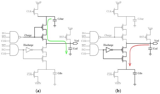
Figure 4.
Charging and discharging of the charge pump. (a) Charge circuit. (b) Discharge circuit.
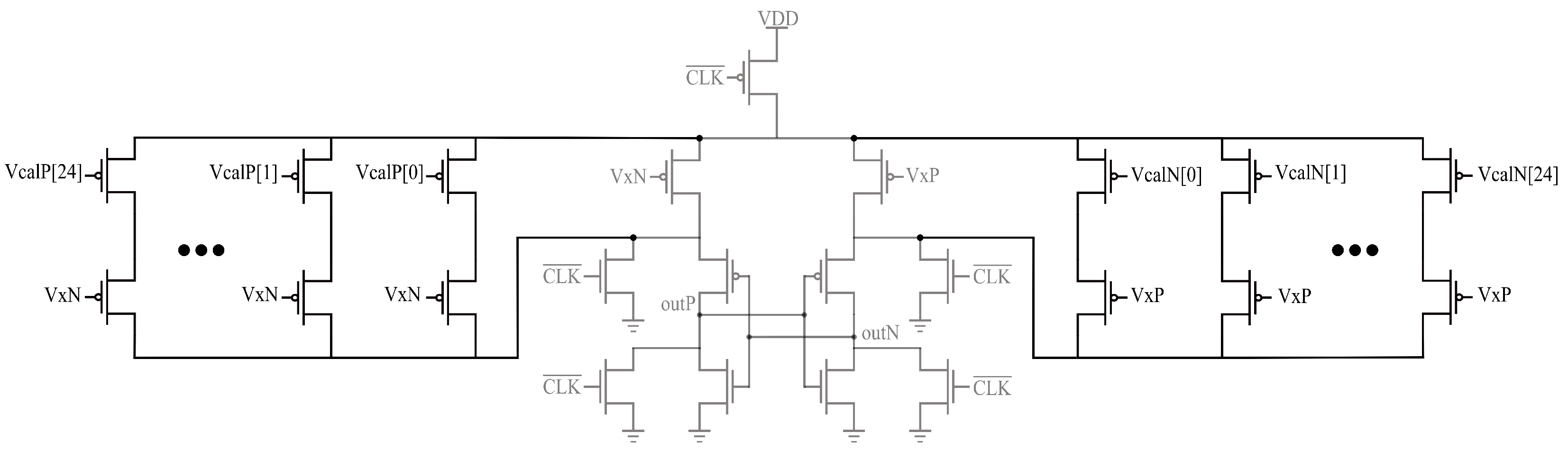
2.2. Calibration Technique: Current Injection via Parallel Transistors
The method described in [21,22] employs current injection through a bank of transistors of different sizes connected in parallel to the input transistors of the output latch, as shown in Figure 5. This method uses 25 pMOS transistors per side, each gated with voltages VxN or VxP. An additional pMOS transistor is connected in series to each of the 25 transistors in the left and right branches (refer to VcalP/VcalN to VcalP/VcalN in Figure 5). These enable/disable the current contribution, allowing for control of the overall injected current.
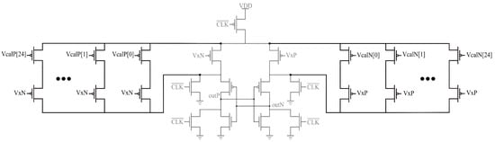
Figure 5.
Additional parallel transistors added to the latch stage.
2.3. Calibration Algorithm
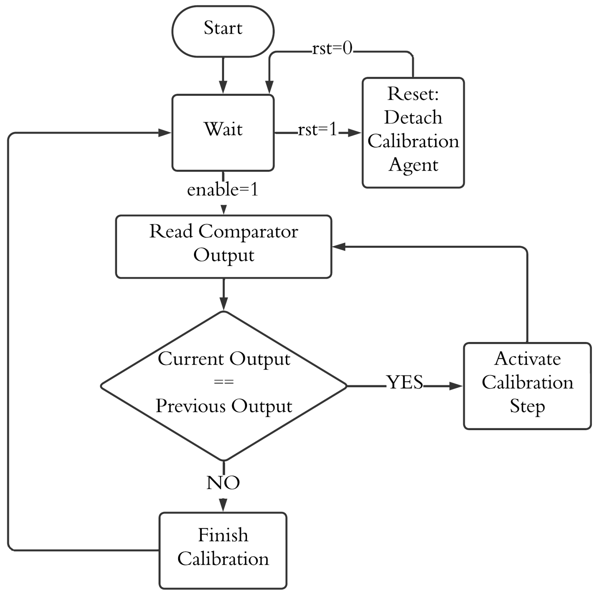
The calibration algorithm employed in [19,20,21,22] and referred to as fast calibration algorithm (FCA) throughout this paper prioritizes speed by completing the calibration process as soon as the first output transition (from an offset-driven output) is detected. This approach minimizes the number of clock cycles required (i.e., fast calibration) at the expense of low precision.
Figure 6 shows the flowchart of the FCA. This method analyzes the comparator outputs to identify the stronger branch (due to mismatch) and subsequently activates the calibration mechanism. After each activation, the outputs are re-evaluated in the next clock cycle. If the output is the same as the previous one, the algorithm continues to perform the calibration process. However, if the output changes, the algorithm considers that the calibration is complete. Note that the FCA does not take into consideration the effects of noise, which could lead to an output change, not necessarily meaning that the comparator is calibrated at a relatively low offset.
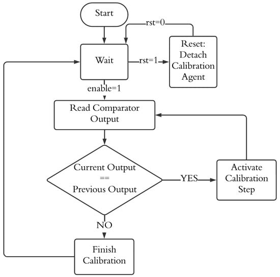
Figure 6.
Fast calibration algorithm (FCA) flowchart.
2.4. Other Calibration Circuitry/Techniques
Nuzzo et al. propose a reference architecture for regenerative comparators in reconfigurable ADC architectures. Specifically, MOS capacitances are used for threshold calibration [25]. Van der Plas et al. present a dynamic offset compensation circuitry in 90 nm for high-speed flash ADC [26]. An offset calibration technique based on an imbalanced load capacitor is presented in [27]. The design, fabricated in 180 nm, offers a solid theoretical foundation to calibrate a two-stage dynamic comparator. Zlochisti et al. present a varactor-based programmable offset compensation of comparators in flash ADCs [28]. Finally, a two-step ADC is presented in [29], where offset calibration is performed using an auxiliary input pair inserted between the first and second stages of a dynamic comparator, with gate voltages controlled by a charge pump circuit.
3. Proposed Offset Calibration Technique
3.1. Offset Compensation Circuitry
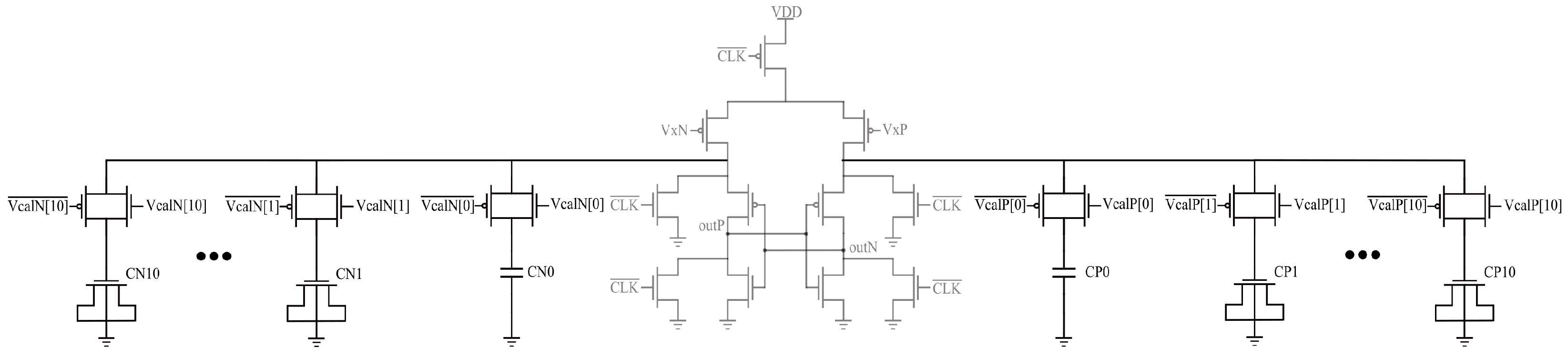
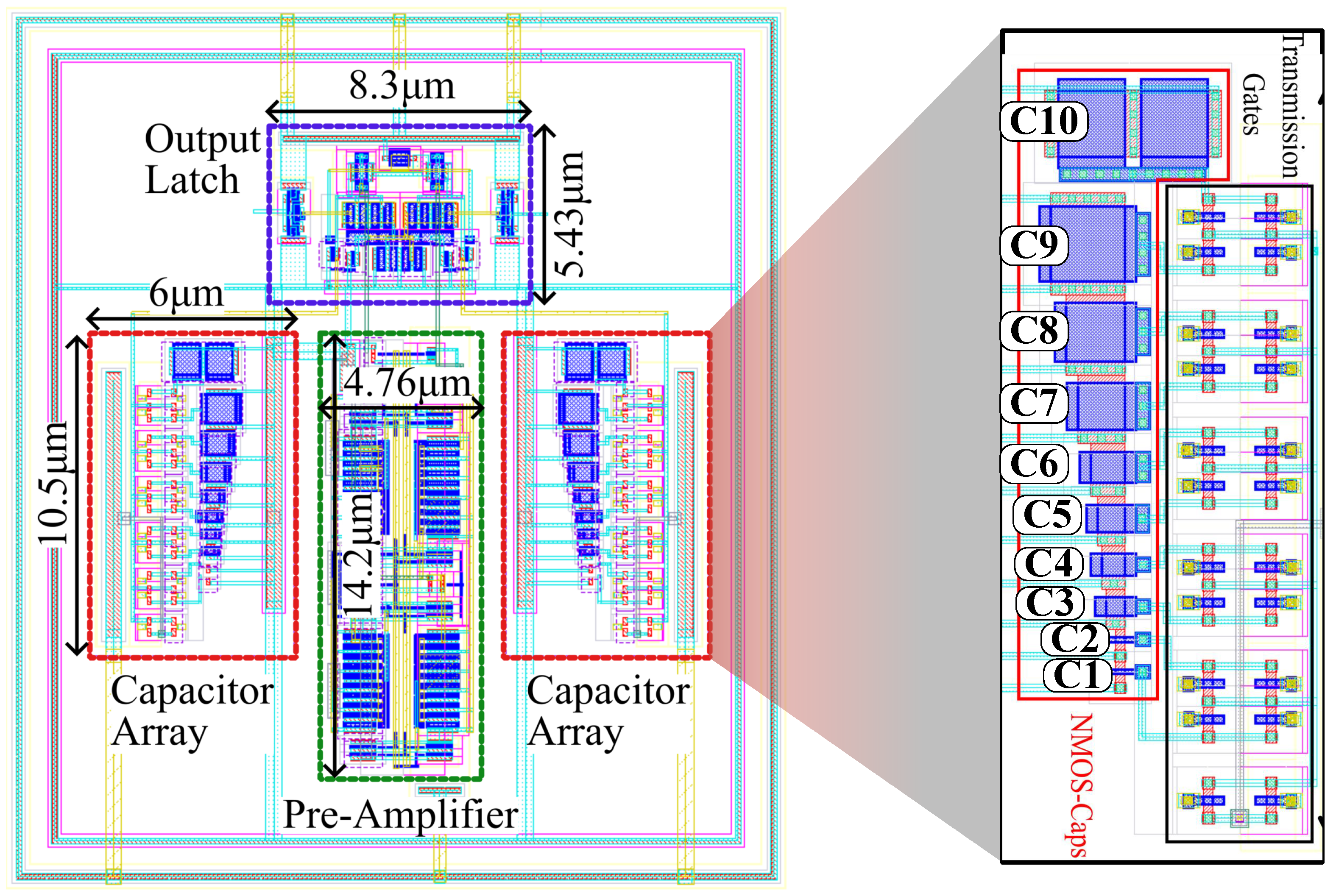
The proposed calibration scheme is mainly based on a load capacitance adjustment method, where the load capacitance is modulated in response to the detected mismatch. At the output latch stage of the dynamic comparator (refer to Figure 1b), 22 capacitors were incorporated to achieve accurate offset compensation, as shown in Figure 7. Specifically, eleven capacitors were placed, in parallel, per side (left and right) of the latch, allowing each capacitor to contribute to the node load through the activation of a transmission gate. This arrangement combines MIM capacitors (CN0 and CP0) with 20 nMOS transistors (CN1-CN10 and CP1-CP10) configured as capacitors (Drain–Source–Bulk connected to the ground).
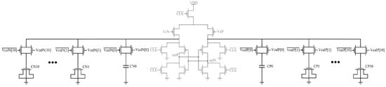
Figure 7.
Capacitive load added to the latch stage of the dynamic comparator.
The 2- offset of the comparator with no calibration arrays was close to 9 mV. We chose this value as the higher boundary of our calibration range. An offset-compensation granularity of 0.5 mV was selected to ensure that the calibration procedure achieves an optimal trade-off between accuracy and silicon-area overhead. MiM capacitors were employed to be the highest offset compensation agent, offering the advantage of saving silicon area, since a larger MOS capacitor was needed to provide the same offset compensation, with the only noticeable downside being a possible routing congestion as the MiMs are placed directly on top of the capacitor array. Regarding transmission gates parasitics, it was found that the capacitance contribution to the output nodes was negligible; the parasitic resistance, on the other hand, had to be compensated by increasing the MOS/MiM capacitors’ dimensions to achieve the desired offset compensation when connecting the capacitors in parallel via the transmission gates.
Table 2 presents the offset compensation steps for different capacitor sizes. Each capacitor compensates for a defined step, with capacitors C1–C6 capable of achieving a compensation of up to 5 mV. For larger compensation requirements, the MIM capacitor C0 serves as a baseline to provide an equivalent 5 mV compensation. Larger capacitors (C7–C10) provide an incremental step of approximately 1 mV each when connected to the MIM capacitor C0. Without the MIM capacitor, achieving similar granularity would require additional nMOS capacitors, resulting in a larger silicon area overhead.
Table 2.
Capacitor size and offset compensation step.
Figure 8 shows the layout of the proposed calibration scheme, including the comparator circuitry. Specifically, the pre-amplifier, output latch, and a capacitor array present area footprints of about 45 m2, 68 m2, and 65 m2, respectively. From the inset in Figure 8, the layout of the calibration circuitry per side comprises 11 transmission gates, 10 nMOS transistors acting as capacitors, and one MIM capacitor. Each MIM capacitor occupies an area of 5.3 m2, with a total of 10.6 m2 for both capacitors.
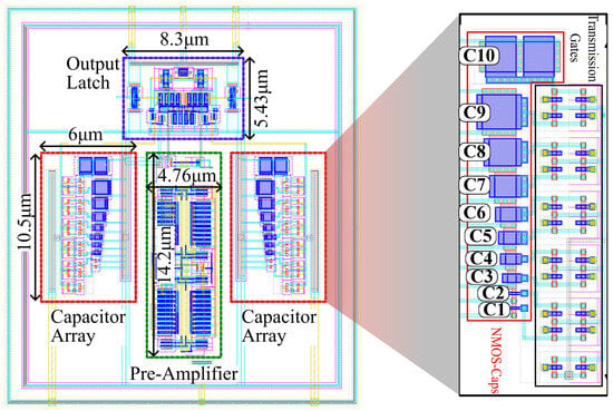
Figure 8.
Layout of the comparator along with calibration circuits.
To determine the offset sign, the inputs of the comparator are shorted to the same voltage, creating a = 0 mV condition. This condition indicates which side (OutP or OutN) is stronger due to mismatch, allowing the circuit to apply the calibration technique. The working principle of the used technique is based on adjusting the output capacitance to account for mismatch. By adding capacitance to the stronger output side, the additional capacitance slows down this side by redirecting current to the capacitor array, allowing the weaker side to catch up. As a result, the offset is reduced.
Note that when the differential input approaches the offset voltage, the outputs of the comparator present sporadic oscillations. This behavior complicates calibration, as relying on the first output transition to signal calibration completion may lead to insufficient compensation. The initial transition could be noise-induced, with subsequent outputs returning to their initial state, failing to achieve proper calibration. To mitigate the effects of noise, this work proposes a calibration algorithm, as described hereafter.
3.2. Window-Based Calibration Algorithm
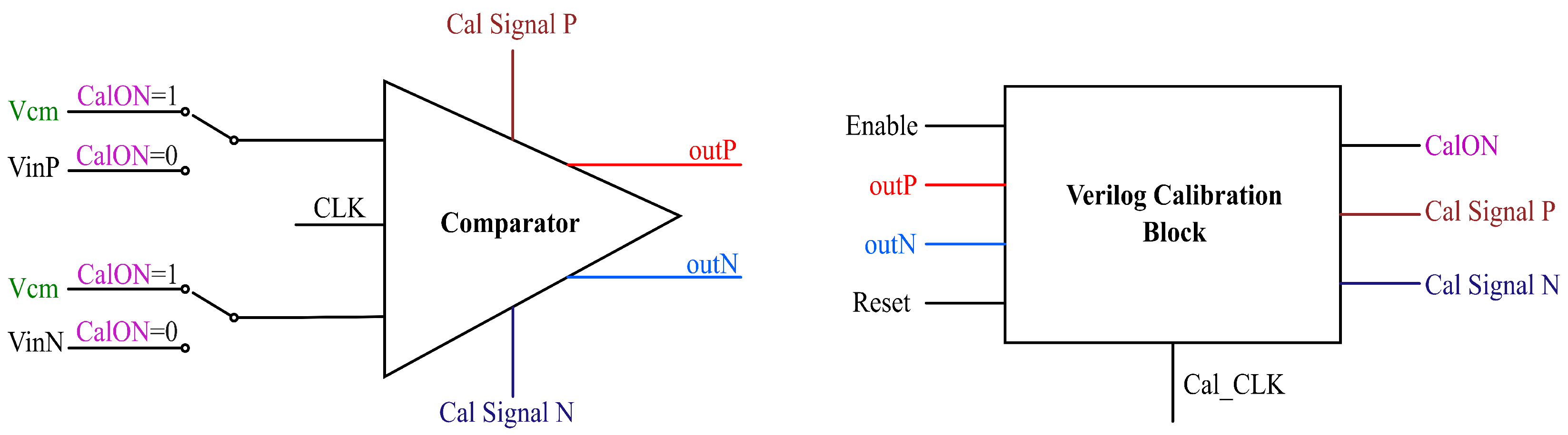
The proposed calibration algorithm evaluates a predetermined number of outputs and analyzes whether the result alternates approximately evenly between the two comparator outputs. This minimizes the impact of noise and ensures a near-zero calibrated offset voltage. The algorithm is implemented in a synthesized Verilog code. Performance is tested using the Analog-Mixed Signal (AMS) simulator in Virtuoso, which performs real-time co-simulation between the digital and analog components [30]. Transient noise was added to achieve more realistic simulation results. Figure 9 shows the AMS simulation setup, where the Verilog-based Calibration Block presents the following input signals: “Enable” that triggers the calibration; “Reset”, which restores the comparator to its pre-calibration state; “outP” and “outN” are the comparator output signals used as feedback signals for the calibration control algorithm; and “Cal_CLK”, a clock signal with the same frequency as the comparator clock but phase-shifted by 1/4 of the period to ensure stable output analysis. The Verilog-based Calibration Block outputs are “CalON”, which connects the comparator inputs to a common-mode voltage when asserted to logic “1” and to VinP and VinN when asserted to logic “0”; “Cal Signal P” and “Cal Signal N” are control signals that activate the compensation technique, i.e., these correspond to signals VcalP[0:11] and VcalN[0:11] in Figure 7, activating transmission gates to connect calibration capacitors.
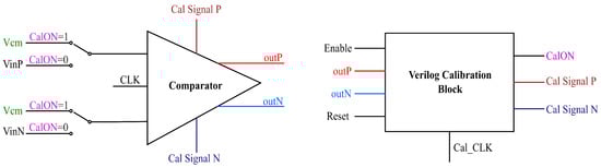
Figure 9.
Simulation setup of the comparator with the calibration block.
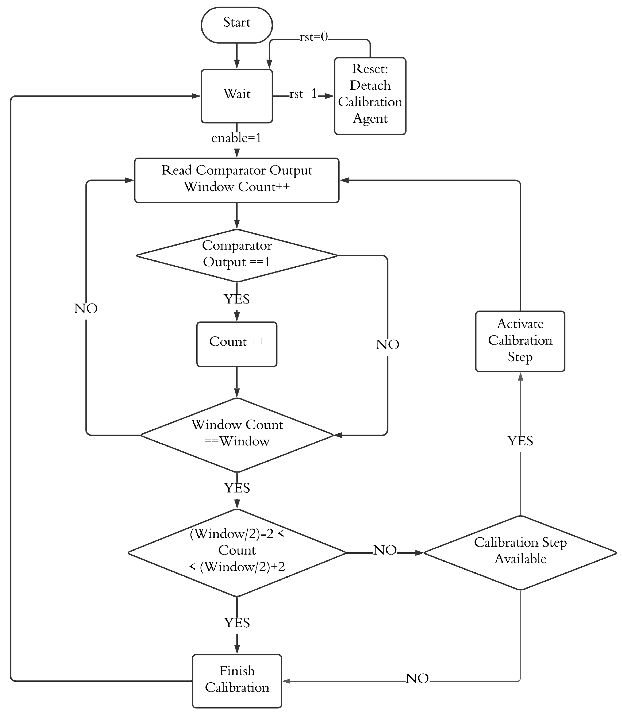
The flowchart in Figure 10 describes the algorithm. In the proposed method, a fixed number of output readings referred to as “Window” is set, and the algorithm triggers the comparator and stores a count of the outputs for “Window” times. Afterward, it checks how many of these outputs are “1” and verifies whether the total “Count” of the values of one falls within a predefined range. This range is set to Window/2 ± 2. For example, if “Window” is set to 22, an acceptable range for “Count” is from 9 to 13, as shown in the flowchart. If the “Count” is outside this range, the algorithm proceeds to the next calibration step and repeats the process until the “Count” falls within the desired range, indicating that the offset of the comparator is sufficiently low for the outputs to toggle between logic “1” and “0” due to noise fluctuations. At this point, the calibration is considered to be completed.

Figure 10.
Flowchart of the window calibration algorithm.
The algorithm convergence depends on the number of calibration steps available and the calibration window. If during the calibration process the algorithm makes use of all the calibration steps without satisfying the window condition, the calibration is completed. Meanwhile, in the cases where the comparator offset is lower than the maximum achievable, it can be compensated, depending on the window condition. For greater values of window condition, the algorithm converges at the cost of calibration accuracy, while for lower values of window condition, the window condition is rarely satisfied. To avoid this, the window condition has to be neither too large nor too short. According to our analysis, the window condition is set to (refer to Figure 10), emerging as an optimal value for the given offset calibration step (≈0.5 mV).
3.3. Functional Verification
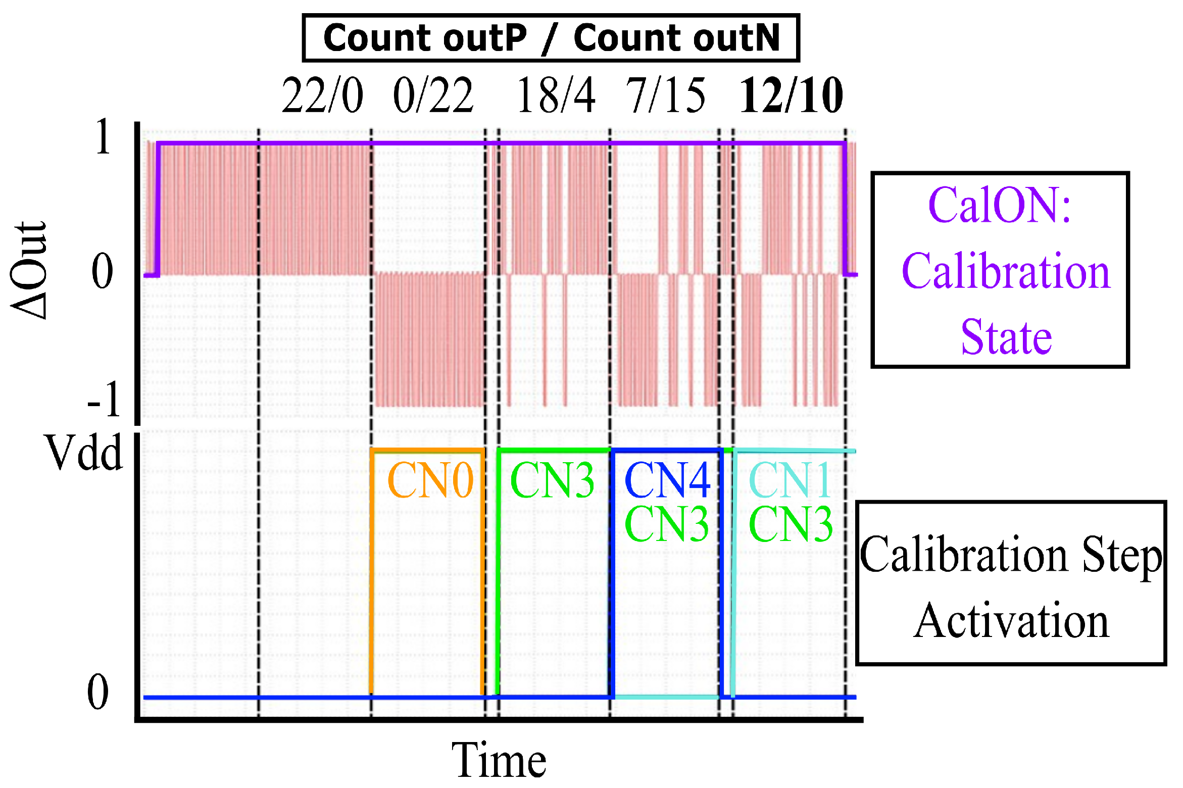
Figure 11 shows functional verification of the proposed scheme (algorithm example waveforms extracted from one Monte Carlo simulation), where the initial offset is about 1.5 mV. During the calibration process, the “CalON” signal is enabled to indicate the start of calibration. This connects the comparator inputs to the same voltage, creating the = 0 condition. In the first window, the “Count” shows outP = 1 occurring 22 times and outN = 1 occurring 0 times, indicating that the offset favors the outP node. This results in the decision to connect the VcalN[0:11] capacitor side (see left side in Figure 7). During the second window, the MIM capacitor (CN0) is connected, but after obtaining an outP = 1 count of 0, CN0 is disconnected due to offset overcompensation.
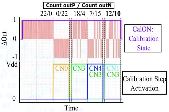
Figure 11.
Window calibration algorithm example simulation. Note: waveforms extracted from one Monte Carlo simulation.
The process then proceeds to add smaller capacitors. In the third window, CN3 is connected, resulting in outP (outN) = 1 occurring 18 (4) times, indicating further adjustment is needed. Then (refer to fourth window), CN4 is connected, but the outP (outN) count drops (rises) to 7 (15), indicating overcompensation again; thereby, CN4 is disconnected. Finally, in the fifth window, the smaller capacitor CN1 is connected, resulting in an outP (outN) count of 12 (10), which falls within the predefined range for calibration. The “CalON” signal is then deactivated, indicating that the calibration is complete.
For the above offset example, the capacitors are CN3 (providing approximately 1 mV compensation) and CN1 (about 0.5 mV compensation).
4. Simulation Results
The proposed design was evaluated and compared with other techniques: (1) current injection via gate biasing controlled by a charge pump circuitry and (2) current injection through parallel transistors. These techniques were applied to the two-stage dynamic comparator (see Figure 1) described in Section 2.
The simulations were performed with two calibration algorithms: the proposed window-based method (refer to Section 3.2) and the FCA (refer to Section 2.3) from the literature. The calibration algorithms were implemented in Verilog, and AMS simulation with added transient noise enabled real-time co-simulation and precise analysis of the interactions between the digital and analog blocks. Each calibration technique was tested using 1000 Monte Carlo post-layout simulations, both before and after calibration, to evaluate how each technique impacts key performance metrics of the comparator. The measured metrics included offset voltage, the number of cycles required for calibration, the average energy consumed during calibration, energy per comparison, delay, input-referred noise, the maximum frequency achievable by the comparator, and the area footprint.
4.1. Offset Voltage and Input-Referred Noise Evaluation Methods
The comparator offset is evaluated under extensive Monte Carlo transient simulations (1000 samples) to statistically capture the effects of random mismatch from process variations across devices. The used evaluation methodology based on [31] is as follows: a Verilog-A differential voltage ramp with two segments, a falling ramp ranging from +15 mV to −15 mV, and a rising ramp ranging from −15 mV to +15 mV in 0.2 mV steps is applied to the the comparator inputs, and all the input voltages are centered around a common-mode voltage of VDD/2. The offset is obtained by identifying the input voltage at which the differential output of the comparator toggled from logic “1” to “0” and from logic “0” to “1” on the falling and rising ramps, respectively. The final offset is calculated as the average of the obtained values in these two transition points.
Input-referred noise is characterized by 1000 transient simulations at each input differential voltage step, sweeping from −7 mV to +7 mV in steps of 0.2 mV. For each input differential voltage value, the comparator is triggered 2000 times. The number of logical ”1”s at the differential output is measured, and the switching probability is calculated based on the 2000 clock cycles. As the increases, the output gradually shifts from having mostly logic “0” to mostly logic “1” due to noise causing occasional incorrect decisions near the switching threshold. The probability curve is then fitted to a cumulative distribution function (CDF) from which the standard deviation is extracted to represent the input-referred noise [25,32,33].
4.2. Offset Voltage Results
Figure 12 summarizes the offset calibration results. It shows the data for each calibration technique in three stages: before calibration, after fast calibration (i.e., FCA), and after window-based calibration. Figures in the first row (a, b and c) correspond to results from the proposed scheme, while the figures in the second row (d, e and f) correspond to the charge pump method. Finally, the third row (g, h, and i) is obtained from the parallel transistors approach.
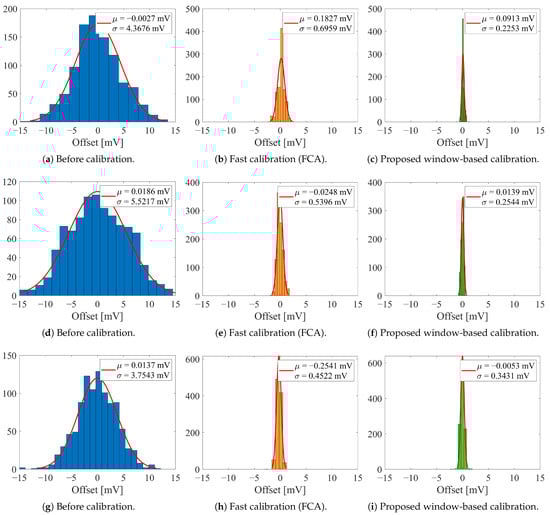
Figure 12.
Offset calibration results. (a–c) Capacitive method (proposed). (d–f) Current injection via gate biasing by charge pump. (g–i) Current injection by parallel transistors.
- Before calibration (Figure 12a,d,g,): A wide spread in offset values with high standard deviations demonstrates the inherent mismatch in the comparator design. Specifically, these results show that the comparator scheme with the parallel transistors array presents the lowest offset overall, while our proposal comes as second best. Finally, the charge pump method exhibits the highest initial offset.
- FCA (Figure 12b,e,h): The offset distribution becomes narrower, indicating that the offset values are less spread out. The lowest of 0.452 mV is observed in the parallel transistors approach, although this method also has the highest average offset. While this calibration method reduces the variation, some spread remains, as this solution relies on a single output toggle to determine the end of the calibration process, resulting in poor offset reduction accuracy. Moreover, there is a significant mean value in the offset after calibration for our proposed capacitor array.
- Proposed window-based calibration (Figure 12c,f,i): The smallest offset distributions, with both lower mean and standard deviation values. This indicates that window-based calibration effectively minimizes offset variation, producing values even lower than the input-referred noise as reported below in Table 3. Our proposed capacitor array and window algorithm solutions yielded the lowest offset-compensated value with a standard deviation of 0.2253 mV, followed by the charge pump circuit with a value of 0.2544 mV, and finally, the parallel transistors approach exhibited 0.3431 mV of compensated offset. For applications requiring precise offset control, window calibration is the preferred approach where the calibration time is not critical.
Among the three techniques, the charge pump method achieves the lowest in offset, providing the most precise calibration. However, this method relies on maintaining a stable voltage on a capacitor to polarize pMOS transistors, and it is vulnerable to leakage over time. These leakage paths cause the stored voltage to gradually decrease, requiring periodic refreshing of the gate voltages to maintain accuracy [21,29,34,35]. As for the capacitive load adjustment technique, it offers a balance between performance and robustness. It achieves the offset calibration without periodic refreshing, since the capacitor array acts as a stable load that is charged and discharged on each clock cycle. This makes it a practical choice for applications that prioritize long-term reliability.
4.3. Performance Metrics
Table 3 summarizes the impact of calibration on the performance metrics of the proposed scheme compared to other current injection schemes. Beyond the calibrated offset voltage described in Section 4.2, other figures of merit are detailed below.
Table 3.
Metric comparison between the proposed offset calibration design and techniques based on current injection. All schemes were designed and laid out considering the 65 nm process.
Table 3.
Metric comparison between the proposed offset calibration design and techniques based on current injection. All schemes were designed and laid out considering the 65 nm process.
| Compensation Technique | Capacitive Load (Proposed) | Current Injection (Charge Pump) | Current Injection (Parallel Transistors) | |||
|---|---|---|---|---|---|---|
| Process [nm] | 65 | 65 | 65 | |||
| Supply Voltage [V] | 1.2 | 1.2 | 1.2 | |||
| Initial Offset Voltage [mV] | 4.37 | 5.52 | 3.75 | |||
| Fast (FCA) | Window (proposed) | Fast (FCA) | Window (proposed) | Fast (FCA) | Window (proposed) | |
| Calibrated Offset Voltage [mV] | = 0.183 = 0.696 | = 0.091 = 0.223 | = −0.025 = 0.539 | = 0.014 = 0.254 | = −0.254 = 0.452 | = −0.005 = 0.343 |
| Calibration Cycles | = 9 = 3 | = 166 = 42 | = 15 = 10 | = 310 = 217 | = 10 = 5 | = 156 = 42 |
| Average Energy per calibration cycle [pJ] | 0.175 | 0.165 | 0.233 | 0.202 | 0.217 | 0.216 |
|
Energy per comparison [pJ] Before calibration | 0.1474 @1 mV 0.1469 @10 mV | 0.131 @1 mV 0.130 @10 mV | 0.172 @1 mV 0.167 @10 mV | |||
|
Delay [ns] Before calibration | 4.09 @1 mV 3.44 @10 mV | 3.39 @1 mV 3.22 @10 mV | 7.36 @1 mV 5.49 @10 mV | |||
|
EDP [pJ·ns] Before calibration | 0.60 @1 mV 0.51 @10 mV | 0.44 @1 mV 0.42 @10 mV | 1.27 @1 mV 0.92 @10 mV | |||
| Noise [V] | 364.6 | 359.8 | 361.1 | |||
| Before calibration | ||||||
|
Energy per comparison [pJ] After calibration | 0.165 @1 mV 0.164 @10 mV | 0.207 @1 mV 0.192 @10 mV | 0.211 @1 mV 0.209 @10 mV | |||
|
Delay [ns] After calibration | 6.78 @1 mV 4.03 @10 mV | 2.69 @1 mV 1.84 @10 mV | 6.94 @1 mV 4.29 @10 mV | |||
|
EDP [pJ·ns] After calibration | 1.12 @1 mV 0.66 @10 mV | 0.56 @1 mV 0.35 @10 mV | 1.46 @1 mV 0.89 @10 mV | |||
| Noise [V] | 365.3 | 392.4 | 345.8 | |||
| After calibration | ||||||
| fmax [MHz] (3-) | 30.23 @1 mV 63.73 @10 mV | 78.60 @1 mV 122.30 @10 mV | 4.97 @1 mV 29.54 @10 mV | |||
| Area [m2] | Transistors: 65 MIMCaps: 10.6 | Transistors: 39 MIMcaps: 1266 | 122 | |||
- Calibration cycles: The number of cycles required to complete calibration varies significantly. Using the FCA, the capacitive and parallel transistor techniques present the lowest cycle counts (9 and 10 cycles, respectively), followed by the charge pump method (15 cycles). However, the window-based algorithm presents a higher and variable cycle count due to its iterative process, required to minimize the offset. Capacitive and parallel transistor techniques complete calibration in 166 and 156 cycles, respectively, while the charge pump method requires 310 cycles, nearly double the others.
- Average calibration energy: The proposed capacitive load technique is the most energy efficient, requiring an average energy per calibration cycle of 0.175 pJ for fast calibration and 0.165 pJ for window-based calibration. The charge pump technique is the least efficient, consuming 0.233 pJ/cycle and 0.202 pJ/cycle for fast and window calibration, respectively. The parallel transistor method lies in between, with 0.217 pJ/cycle for fast calibration and 0.216 pJ/cycle for the window-based algorithm. Note that the proposed window-based approach requires a higher number of calibration cycles compared to the FCA-based compensation techniques. Therefore, the overall energy consumed during the entire calibration process is higher.
- Energy per comparison and delay (refer to highlighted results in Table 3): Energy values with no calibration applied are lowest for the charge pump technique (0.131 pJ at = 1 mV), followed by the capacitive load technique (0.147 pJ at = 1 mV) and the parallel transistors technique consuming the most energy (0.172 pJ at = 1 mV). After calibration, energy consumption increases for all methods, with the current injection methods consuming more energy than the capacitive load technique. In terms of delay, the charge pump technique achieves the lowest delay, showing a delay of 3.39 ns and 2.69 ns at = 1 mV, with and without calibration, respectively. Our proposed solution achieves a post-calibration delay of 6.78 ns, compared to 4.09 ns with no calibration applied. On the other hand, the parallel transistors technique has the highest delay after calibration (6.94 ns at = 1 mV). Using either the charge pump or parallel transistors approaches results in a delay performance increase compared to the operation with no offset compensation. This improvement is a consequence of the nature of these methodologies, which involve a current injection that increases the drive strength of the output latch.
- Energy-Delay Product, EDP (refer to highlighted results in Table 3): The charge pump technique achieves the lowest EDP at = 1 mV, with calibration (0.56 pJ·ns) and without calibration (0.44 pJ·ns), indicating high efficiency. The capacitive load technique also achieves a relatively low EDP without calibration (0.60 pJ·ns at = 1 mV); however, after calibration, its EDP increases due to the longer delay, although it improves (decreases) as increases. In contrast, the parallel transistors approach has the highest EDP, making it less efficient when balancing energy consumption and speed.
- Power consumption: Power consumption is evaluated with a clock period of 200 and a = 1 mV. Prior calibration, the obtained average power consumption per comparison by employing the parallel transistors technique is 0.860 W, the capacitive load method follows with a consumption of 0.737 W, while the charge pump approach consumes 0.655 W. After calibration, the obtained power consumption is 1.055 W for the parallel transistors, 1.035 W for the charge pump method, and 0.825 W for the capacitive load method, which remains the most power efficient technique.
- Noise performance (refer to highlighted results in Table 3): Prior to calibration, all techniques present similar levels of noise. However, the impact of calibration on noise varies across methods. The capacitive load presents an slight increase ab about 1 V. The parallel transistors approach achieves a reduction of 15 V in noise. As for the charge pump technique, it presents the most significant noise degradation, with an increase of 32 V, which may be a concern for noise-sensitive designs
- Maximum operating frequency: The maximum frequency is calculated as the inverse of twice the propagation delay, obtained under 1000 Monte Carlo samples, and reported at 3- in Table 3. The charge pump method presents the highest operation frequency (122.3 MHz at = 10 mV), making it the most suitable for high-speed applications. The proposed capacitive load approach operates at a maximum frequency of 63.73 MHz at = 10 mV. The parallel transistors method presents the lowest maximum frequency (29.54 MHz), which is a trade-off to achieve an accurate calibration of the offset voltage as it needs more transistors to provide a smaller calibration step at the expense of longer delay.
- Area overhead: The charge pump method presents and area-footprint of about 1305 m2, from which 1266 m2 is due to the MIM capacitors. The proposed capacitive load method occupies a total area footprint of about 75.6 m2, the lowest among the other calibration techniques.
4.4. Process, Voltage, and Temperature Variation Analysis
Process–Voltage–Temperature (PVT) analysis was performed under exhaustive Monte Carlo simulations (1000 samples) for the proposed calibration solution along with current injection schemes. Specifically, we report offset, delay, energy, and EDP before and after compensation. Simulations were carried out for Slow–Slow (SS) and Fast–Fast (FF) processes, with a ±10% VDD variation and two temperature points (0 °C and 80 °C): SS-1.08V-80 °C and FF-1.32V-0 °C. The results are presented along with the Typical–Typical case values (TT-1.2V-27 °C) discussed in Section 4.3.
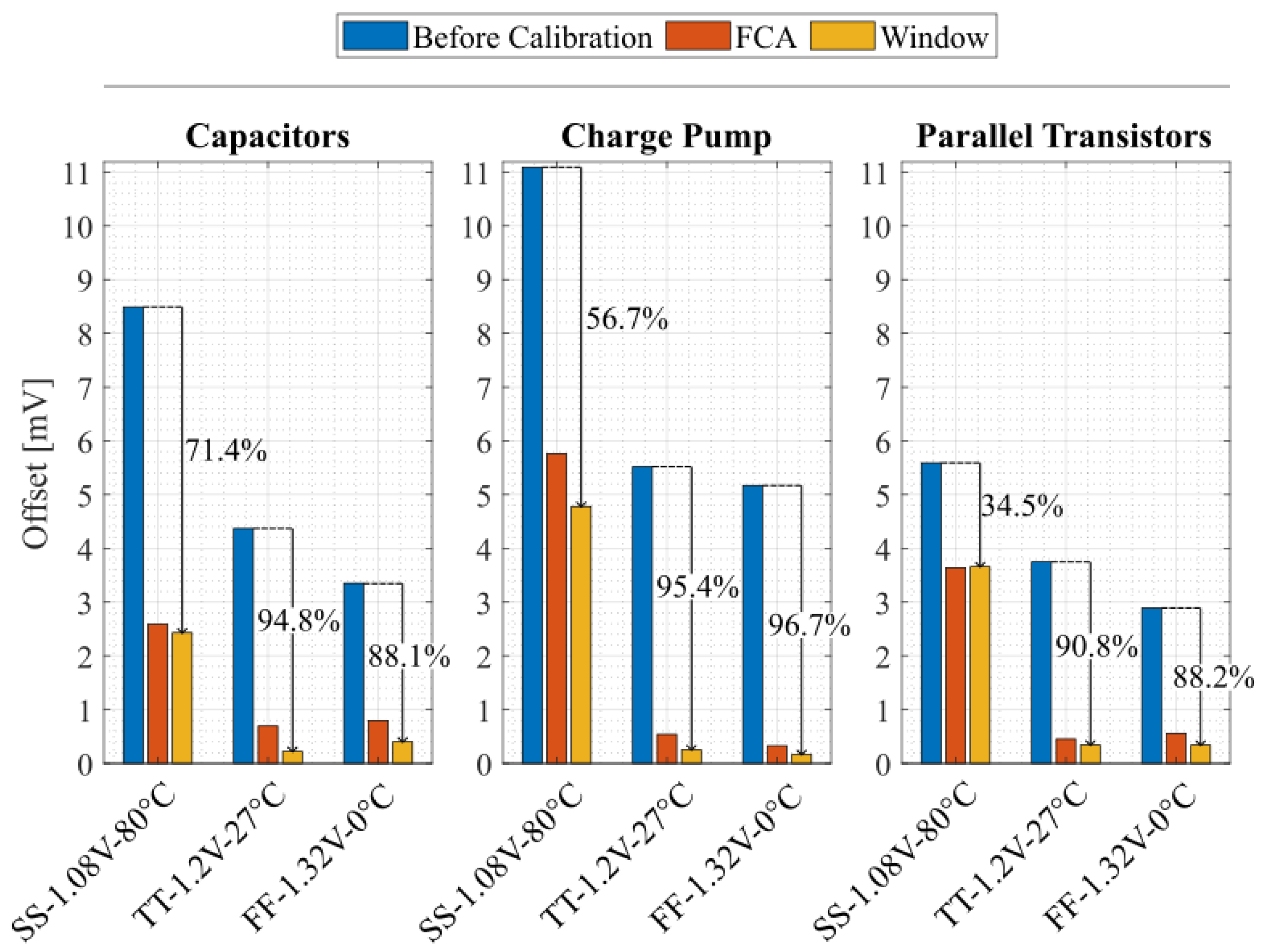
Figure 13 shows the offset under PVT variations. The offset at the SS corner increases compared to the typical case. The proposed capacitive load technique shows a 71.4% offset improvement using the window algorithm and a 69.5% reduction employing the FCA. The charge pump technique while employing FCA and window algorithms showed 48% and 56.7% improvement, respectively. Parallel transistors approach results were similar for both FCA and window algorithms, with 34.8% and 34.5% offset reduction, respectively. The FF corner showed a slightly reduced offset with respect to the TT case. After compensation by applying the window algorithm, the offset reduction employing the proposed capacitive load scheme was 88.1%. Meanwhile, by applying the FCA, the offset reduction was 76.1%. The charge pump technique also benefited more from the window algorithm in this corner, showing an offset reduction of 96.7%, while for the FCA, the reduction was 93.6%. Finally, with the parallel transistors approach, the window algorithm presented an 88.2% offset reduction and FCA 80.7%.
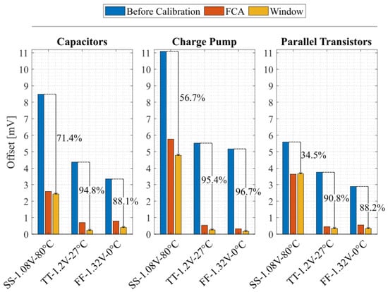
Figure 13.
Offset values before and after calibration, for both fast and window algorithms under PVT variations.
Overall, both algorithms provide a considerable offset compensation, with the window algorithm allowing more precise compensation over FCA in most cases. In absolute numbers, when applying our proposed window algorithm to the capacitive load, charge pump, and parallel transistors approaches, the resulting offset is 2.43 mV, 4.78 mV, and 3.66 mV in the SS corner, respectively. For the FF corner, a 0.39 mV offset-compensated value was obtained by employing the capacitive load technique, while with the charge pump approach, a 0.16 mV offset was measured. When using the parallel transistors approach the obtained offset value was 0.34 mV. Our proposed calibration technique based on capacitive load achieves the lowest offset among competitors in the SS corner. In the FF corner, the charge pump approach performs best, followed by the parallel transistors method, with our proposed solution placed closely behind by a small margin.
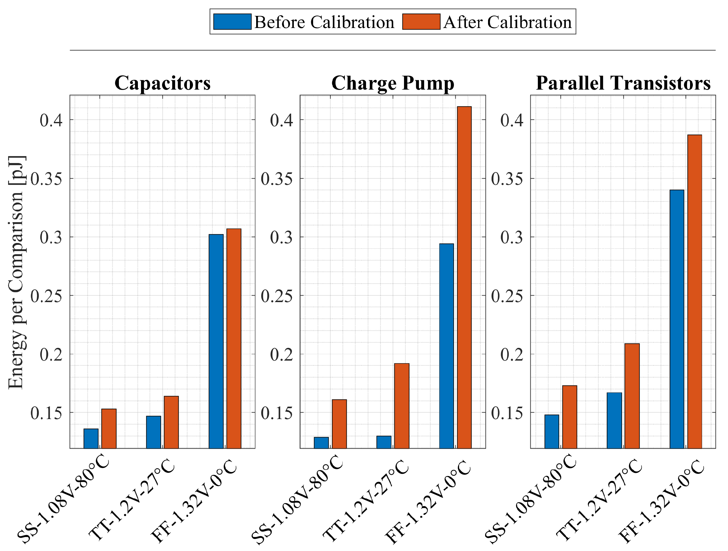
Figure 14 shows the average energy per comparison before and after offset calibration using the window algorithm across the three PVT corners. The FCA algorithm presents similar () energy consumption. In the SS corner, energy consumption increases of 12.5%, 24.8%, and 16.89% are noticed in the capacitive load, charge pump, and parallel transistors approach, respectively. Results in the FF corner reveal that our proposed technique presents a small energy consumption increase of 1.65% after offset compensation. When using the charge pump approach, there is a noticeable increase of 39.79%. By employing the parallel transistors technique, an increase of 13.8% is observed. In terms of energy consumption overhead produced by the calibration circuitry, our proposed solution demonstrates best performance under PVT variations.
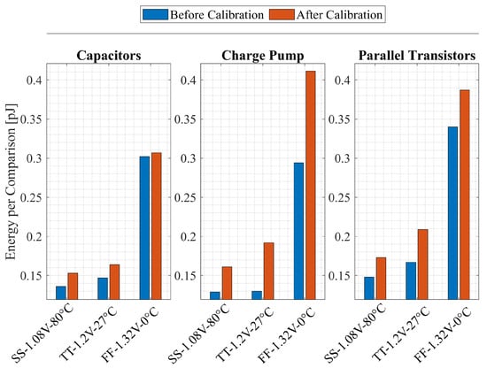
Figure 14.
Energy values before and after calibration under PVT variations for a = 10 mV.
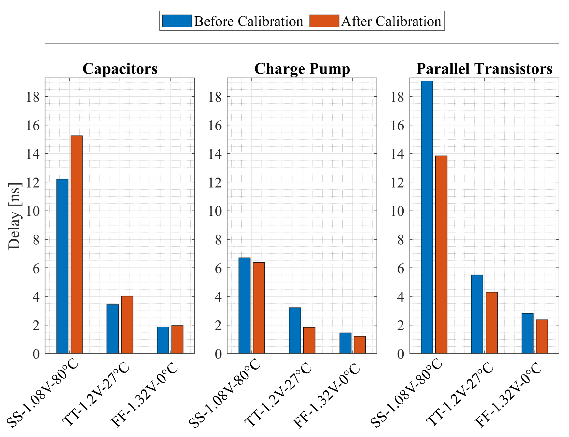
Figure 15 shows the delay under PVT variations. Delay performance is best when employing the charge pump circuit, resulting in a post-calibration delay of 6.38 ns and 1.21 ns in the SS and FF corners, respectively, followed by the parallel transistors approach, which exhibits 13.84 ns and 2.38 ns. Both techniques show a delay reduction after calibration. Finally, our proposed solution exhibits a post-calibration delay of 15.26 ns in the SS corner and 1.97 ns in the FF corner.

Figure 15.
Delay results before and after calibration under PVT variations for a = 10 mV.
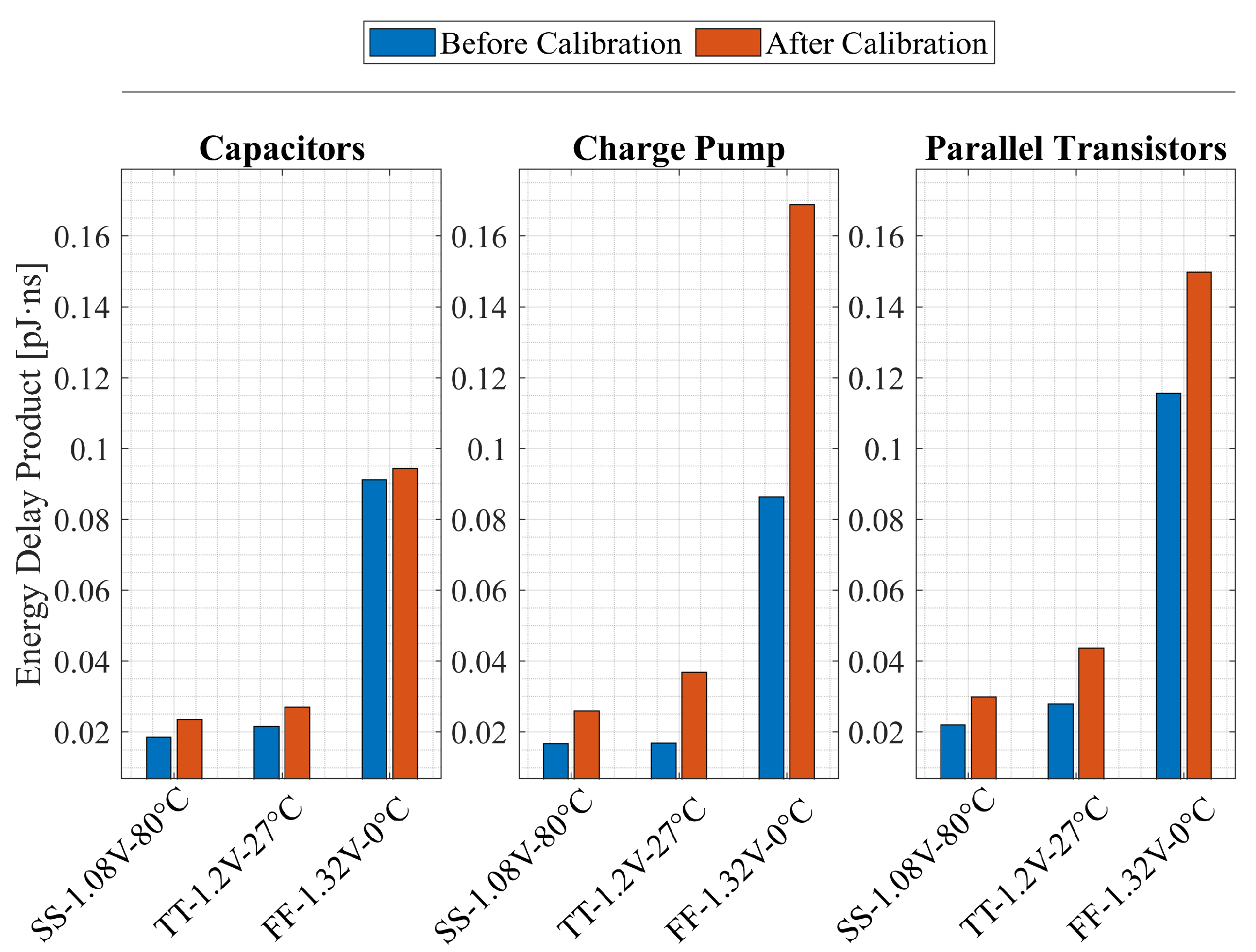
In Figure 16, the EDP is reported across PVT variations. After calibration in the SS corner, the proposed capacitor load solution exhibits the lowest amount of 0.023 pJ·ns, followed by charge pump and parallel transistors approaches with values of 0.26 pJ·ns and 0.3 pJ·ns, respectively. Results for the FF corner after calibration reveal an increased EDP across all techniques, where our proposed solution shows a major advantage compared to the current injection methods. Specifically, our solution exhibits 0.094 pJ·ns against 0.168 pJ·ns and 0.15 pJ·ns presented by charge pump and parallel transistors approaches, respectively.
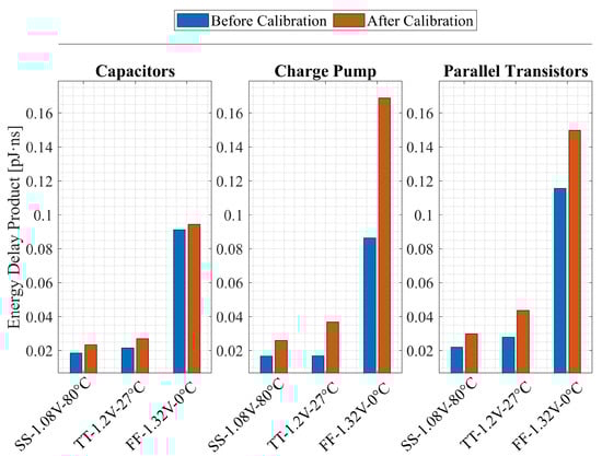
Figure 16.
EDP results before and after calibration under PVT variations.
4.5. Summary
The charge pump method offers the best energy-delay product; however, the capacitor leakage over time is a drawback that limits its long-term accuracy. The proposed capacitive load approach performed best overall, reducing offset to 0.223 mV with the proposed window algorithm, without a recalibration requirement. The combination of MIM and nMOS capacitors allowed a reduced silicon area footprint and provided precise calibration steps without the need for more capacitors.
The window-based algorithm was demonstrated to be more effective than the FCA, improving offset calibration across all techniques. This improvement highlights the benefits of statistical averaging in mitigating the impact of noise during calibration, which is particularly evident in scenarios where the comparator outputs can oscillate due to noise.
5. Conclusions
This work proposes an accurate and low-complexity offset calibration methodology, providing a specific design strategy for dynamic comparators. The best energy-delay product is achieved by the charge pump offset calibration scheme. However, it presents lower long-term accuracy, mainly because of its capacitor leakage. The proposed scheme demonstrates superior performance in offset reduction, achieving a one-sigma offset of 0.223 mV while maintaining a more precise calibration compared to other schemes. Among the calibration algorithms, the proposed window-based algorithm presents robustness against noise-induced variations during the calibration stage.
Author Contributions
Conceptualization, J.C., B.Z., E.G., L.M.P. and M.L.; investigation, J.C. and B.Z.; writing—review and editing, J.C., B.Z., E.G., L.M.P. and M.L. All authors have read and agreed to the published version of the manuscript.
Funding
This work was supported by the Italian Ministry of University and Research (MUR) under grant number SOE_20240000022.
Data Availability Statement
The original contributions presented in this study are included in the article. Further inquiries can be directed to the corresponding author(s).
Conflicts of Interest
The authors declare no conflicts of interest.
References
- Hershberg, B.; Dermit, D.; van Liempd, B.; Martens, E.; Markulić, N.; Lagos, J.; Craninckx, J. A 4-GS/s 10-ENOB 75-mW Ringamp ADC in 16-nm CMOS With Background Monitoring of Distortion. IEEE J.-Solid-State Circuits 2021, 56, 2360–2374. [Google Scholar] [CrossRef]
- Goll, B.; Zimmermann, H. Comparators in Nanometer CMOS Technology; Springer: Berlin/Heidelberg, Germany, 2015; Volume 50, p. 250. [Google Scholar] [CrossRef]
- Hung, W.P.; Chang, C.H.; Lee, T.H. Real-Time and Noncontact Impulse Radio Radar System for μm Movement Accuracy and Vital-Sign Monitoring Applications. IEEE Sens. J. 2017, 17, 2349–2358. [Google Scholar] [CrossRef]
- Sakr, A.; Hussein, A.I.; Fahmy, G.A.; Abdelghany, M.A. High-Speed Comparator Design for RF-to-Digital Receivers. In Proceedings of the 2020 37th National Radio Science Conference (NRSC), Cairo, Egypt, 8–10 September 2020; pp. 207–215. [Google Scholar] [CrossRef]
- Fan, H.; Li, J.; Maloberti, F. Order statistics and optimal selection of unit elements in DACs to enhance the static linearity. IEEE Trans. Circuits Syst. I Regul. Pap. 2020, 67, 2193–2203. [Google Scholar] [CrossRef]
- Gagliardi, F.; Scintu, D.; Piotto, M.; Bruschi, P.; Dei, M. Static-Linearity Enhancement Techniques for Digital-to-Analog Converters Exploiting Optimal Arrangements of Unit Elements. IEEE Trans. Very Large Scale Integr. (VLSI) Syst. 2024, 32, 2243–2256. [Google Scholar] [CrossRef]
- Renteria-Pinon, M.; Tang, X.; Tang, W. Real-Time In-Sensor Slope Level-Crossing Sampling for Key Sampling Points Selection for Wearable and IoT Devices. IEEE Sens. J. 2023, 23, 6233–6242. [Google Scholar] [CrossRef]
- Zhao, X.; Li, D.; Zhang, X.; Liu, S.; Zhu, Z. A 0.6-V 94-nW 10-Bit 200-kS/s Single-Ended SAR ADC for Implantable Biosensor Applications. IEEE Sens. J. 2022, 22, 17904–17913. [Google Scholar] [CrossRef]
- Shifman, Y.; Shor, J. An 11 uW, 0.08 mm2, 125 dB-Dynamic-Range Current-Sensing Dynamic CT Zoom ADC. IEEE Trans. Circuits Syst. I: Regul. Pap. 2024, 71, 3489–3501. [Google Scholar] [CrossRef]
- Chen, P.; Zhao, W.; Wu, M.; Shen, L.; Jia, T.; Huang, R.; Ye, L.; Ma, Y. A 22-nm Delta–Sigma Computing-In-Memory SRAM Macro With Near-Zero-Mean Outputs and LSB-First ADCs for Edge AI Processing. IEEE J.-Solid-State Circuits 2025. [Google Scholar] [CrossRef]
- Tagata, H.; Sato, T.; Awano, H. Double MAC on a Cell: A 22-nm 8T-SRAM Based Analog In-Memory Accelerator for Binary/Ternary Neural Networks Featuring Split Wordline. IEEE Open J. Circuits Syst. 2024, 5, 328–340. [Google Scholar] [CrossRef]
- Li, T.; Huang, J.; Zeng, J.; Guo, C.; Zhang, W.; Fu, X.; Xu, D.; Yan, G.; Jiang, J.; Lai, R.; et al. A digital background calibration method for SAR ADC based on dual-layer feedforward neural network. Microelectron. J. 2025, 159, 106645. [Google Scholar] [CrossRef]
- Kim, S.; Kim, S.; Um, S.; Kim, S.; Kim, K.; Yoo, H.J. Neuro-CIM: ADC-Less Neuromorphic Computing-in-Memory Processor With Operation Gating/Stopping and Digital–Analog Networks. IEEE J.-Solid-State Circuits 2023, 58, 2931–2945. [Google Scholar] [CrossRef]
- Rafiq, M.; Chatterjee, S.; Kumar, S.; Singh Chauhan, Y.; Sahay, S. Utilizing Dual-Port FeFETs for Energy-Efficient Binary Neural Network Inference Accelerators. IEEE Trans. Electron Devices 2024, 71, 4381–4388. [Google Scholar] [CrossRef]
- Qi, X.; Zhao, J.; Lou, Y.; Wang, G.; Tang, K.T.; Li, Y. A 5.3 pJ/Spike CMOS Neural Array Employing Time-Modulated Axon-Sharing and Background Mismatch Calibration Techniques. IEEE Trans. Biomed. Circuits Syst. 2023, 17, 286–298. [Google Scholar] [CrossRef]
- Sangeetha, R.; Vidhyashri, A.; Reena, M.; Sudharshan, R.B.; govindan, S.; Ajayan, J. An Overview Of Dynamic CMOS Comparators. In Proceedings of the 2019 5th International Conference on Advanced Computing Communication Systems (ICACCS), Coimbatore, India, 15–16 March 2019; pp. 1001–1004. [Google Scholar] [CrossRef]
- Tang, X.; Shen, L.; Kasap, B.; Yang, X.; Shi, W.; Mukherjee, A.; Pan, D.Z.; Sun, N. An Energy-Efficient Comparator With Dynamic Floating Inverter Amplifier. IEEE J.-Solid-State Circuits 2020, 55, 1011–1022. [Google Scholar] [CrossRef]
- Razavi, B. The StrongARM latch [A Circuit for All Seasons]. IEEE Solid-State Circuits Mag. 2015, 7, 12–17. [Google Scholar] [CrossRef]
- Tsirmpas, G.; Kontelis, S.; Souliotis, G.; Plessas, F. A high-speed dynamic comparator with automatic offset calibration. AEU-Int. J. Electron. Commun. 2024, 186, 155472. [Google Scholar] [CrossRef]
- Jaiswal, S.K.; Mondal, A.; Srimani, S.; Das, S.; Ghosh, K.; Rahaman, H. Design of a low power, high speed self calibrated dynamic latched comparator. In Proceedings of the 2020 International Symposium on Devices, Circuits and Systems (ISDCS), Howrah, India, 4–6 March 2020; pp. 1–6. [Google Scholar] [CrossRef]
- Lee, J.; Lim, Y.; Sung, B.; Oh, S.; Chun, J.H.; Lee, J. An Effective Transconductance Controlled Offset Calibration for Dynamic Comparators. In Proceedings of the 2020 IEEE International Symposium on Circuits and Systems (ISCAS), Virtual Conference, 14–21 October 2020; pp. 1–5. [Google Scholar] [CrossRef]
- Sharma, N.; Srivastava, R.K.; Hande, V.; Sehgal, D.; Das, D.M. A Self-Calibration Logic Circuit Agnostic To Offset Calibration Technique For High-Precision Dynamic Comparator. In Proceedings of the 2023 IEEE Women in Technology Conference (WINTECHCON), Bangalore, India, 21 September 2023; pp. 1–6. [Google Scholar] [CrossRef]
- Ahrar, A.; Yavari, M. A Digital Method for Offset Cancellation of Fully Dynamic Latched Comparators. In Proceedings of the 2021 29th Iranian Conference on Electrical Engineering (ICEE), Tehran, Iran, 18–20 May 2021; pp. 143–148. [Google Scholar] [CrossRef]
- Yousefirad, M.; Yavari, M. Kick-back Noise Reduction and Offset Cancellation Technique for Dynamic Latch Comparator. In Proceedings of the 2021 29th Iranian Conference on Electrical Engineering (ICEE), Tehran, Iran, 18–20 May 2021; pp. 149–153. [Google Scholar] [CrossRef]
- Nuzzo, P.; De Bernardinis, F.; Terreni, P.; Van der Plas, G. Noise analysis of regenerative comparators for reconfigurable ADC architectures. IEEE Trans. Circuits Syst. I Regul. Pap. 2008, 55, 1441–1454. [Google Scholar] [CrossRef]
- Van der Plas, G.; Decoutere, S.; Donnay, S. A 0.16 pJ/conversion-step 2.5 mW 1.25 GS/s 4b ADC in a 90 nm digital CMOS process. In Proceedings of the 2006 IEEE International Solid State Circuits Conference-Digest of Technical Papers, San Francisco, CA, USA, 6–9 February 2006; p. 2310. [Google Scholar]
- Li, D.; Meng, Q.; Li, F.; Wang, L. An analysis of offset calibration based additional load capacitor imbalance for two-stage dynamic comparator. In Proceedings of the 2016 6th International Conference on Information Communication and Management (ICICM), Hatfield, UK, 29–31 October 2016; pp. 264–267. [Google Scholar]
- Zlochisti, M.; Zahrai, S.A.; Onabajo, M. Digitally programmable offset compensation of comparators in flash ADCs for hybrid ADC architectures. In Proceedings of the 2015 IEEE 58th International Midwest Symposium on Circuits and Systems (MWSCAS), Fort Collins, CO, USA, 2–5 August 2015; pp. 1–4. [Google Scholar]
- Figueiredo, P.M.; Cardoso, P.; Lopes, A.; Fachada, C.; Hamanishi, N.; Tanabe, K.; Vital, J. A 90 nm CMOS 1.2 v 6b 1GS/s two-step subranging ADC. In Proceedings of the 2006 IEEE International Solid State Circuits Conference-Digest of Technical Papers, San Francisco, CA, USA, 5–9 February 2006; pp. 2320–2329. [Google Scholar]
- Castaldo, E.; Gibilaro, M.E. A Comprehensive Analog–Mixed Signal (AMS) Simulations Environment. Chips 2024, 3, 258–270. [Google Scholar] [CrossRef]
- Graupner, A.; Sobe, U. Offset-Simulation of Comparators. Core—An Open Scholarly Infrastructure for Researchers 2007. Available online: https://nbn-resolving.org/urn:nbn:de:swb:ch1-200700897 (accessed on 30 October 2024).
- Chevella, S.; O’Hare, D.; O’Connell, I. A low-power 1-V supply dynamic comparator. IEEE Solid-State Circuits Lett. 2020, 3, 154–157. [Google Scholar] [CrossRef]
- Satpathy, B.; Srivastava, U.; Kaur, A. An Asymmetric Dynamic Comparator for Low Offset, Low Noise and High Speed Applications. IEEE Trans. Instrum. Meas. 2025, 55, 2003508. [Google Scholar] [CrossRef]
- Pan, F.; Pham, T. Capacitive Regulation of Charge Pumps Without Refresh Operation interruption. US Patent 9,077,238, 7 July 2015. [Google Scholar]
- Ballo, A.; Grasso, A.D.; Palumbo, G. A memory-targeted dynamic reconfigurable charge pump to achieve a power consumption reduction in IoT nodes. IEEE Access 2021, 9, 41958–41964. [Google Scholar] [CrossRef]

Disclaimer/Publisher’s Note: The statements, opinions and data contained in all publications are solely those of the individual author(s) and contributor(s) and not of MDPI and/or the editor(s). MDPI and/or the editor(s) disclaim responsibility for any injury to people or property resulting from any ideas, methods, instructions or products referred to in the content. |
© 2025 by the authors. Licensee MDPI, Basel, Switzerland. This article is an open access article distributed under the terms and conditions of the Creative Commons Attribution (CC BY) license (https://creativecommons.org/licenses/by/4.0/).