A 0.8 V Low-Power Wide-Tuning-Range CMOS VCO for 802.11ac and IoT C-Band Applications


Abstract
1. Introduction
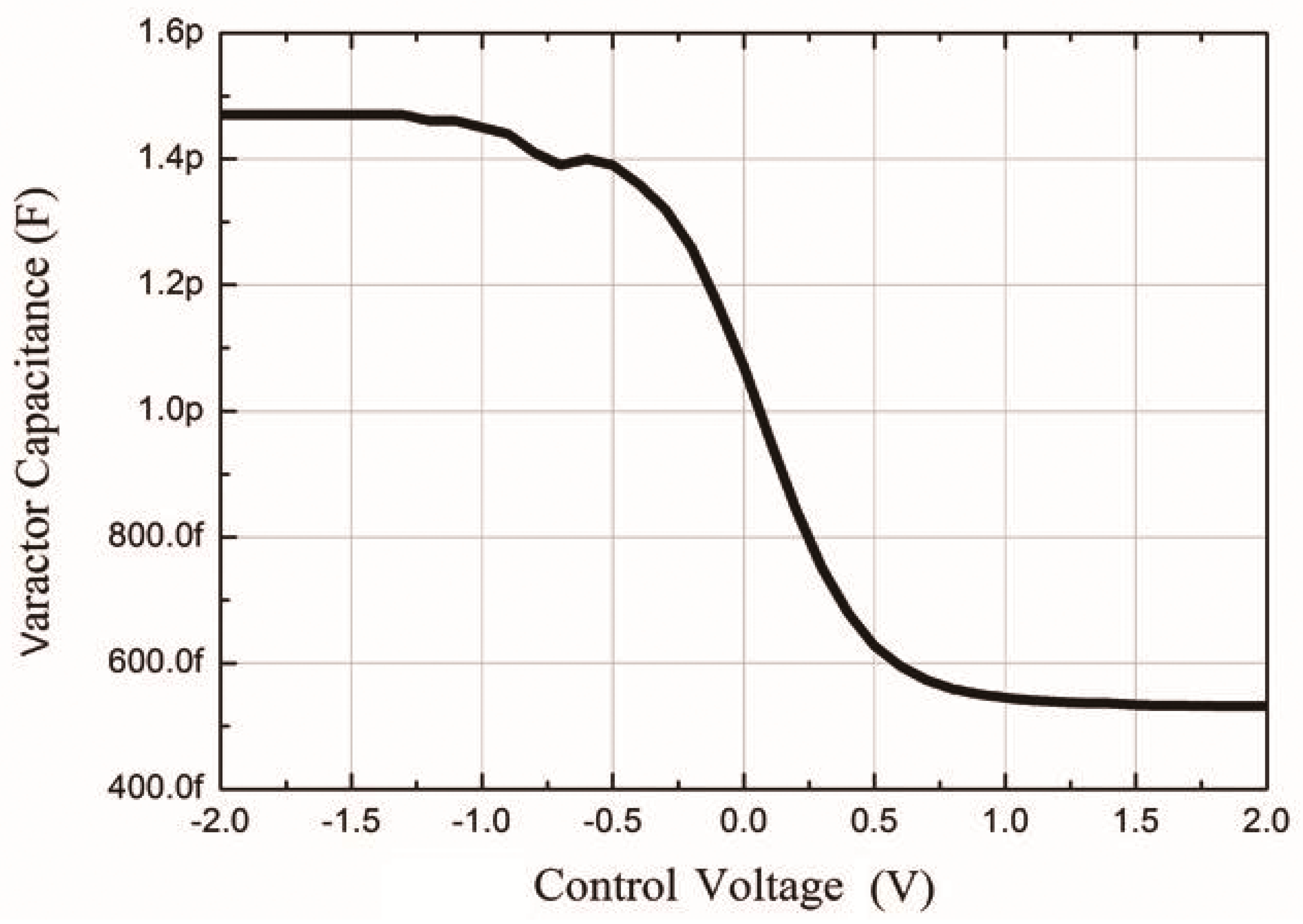
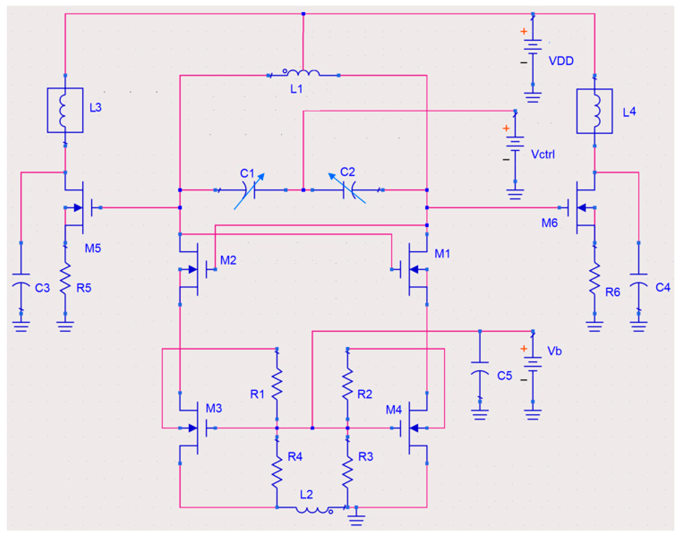
2. VCO Architecture
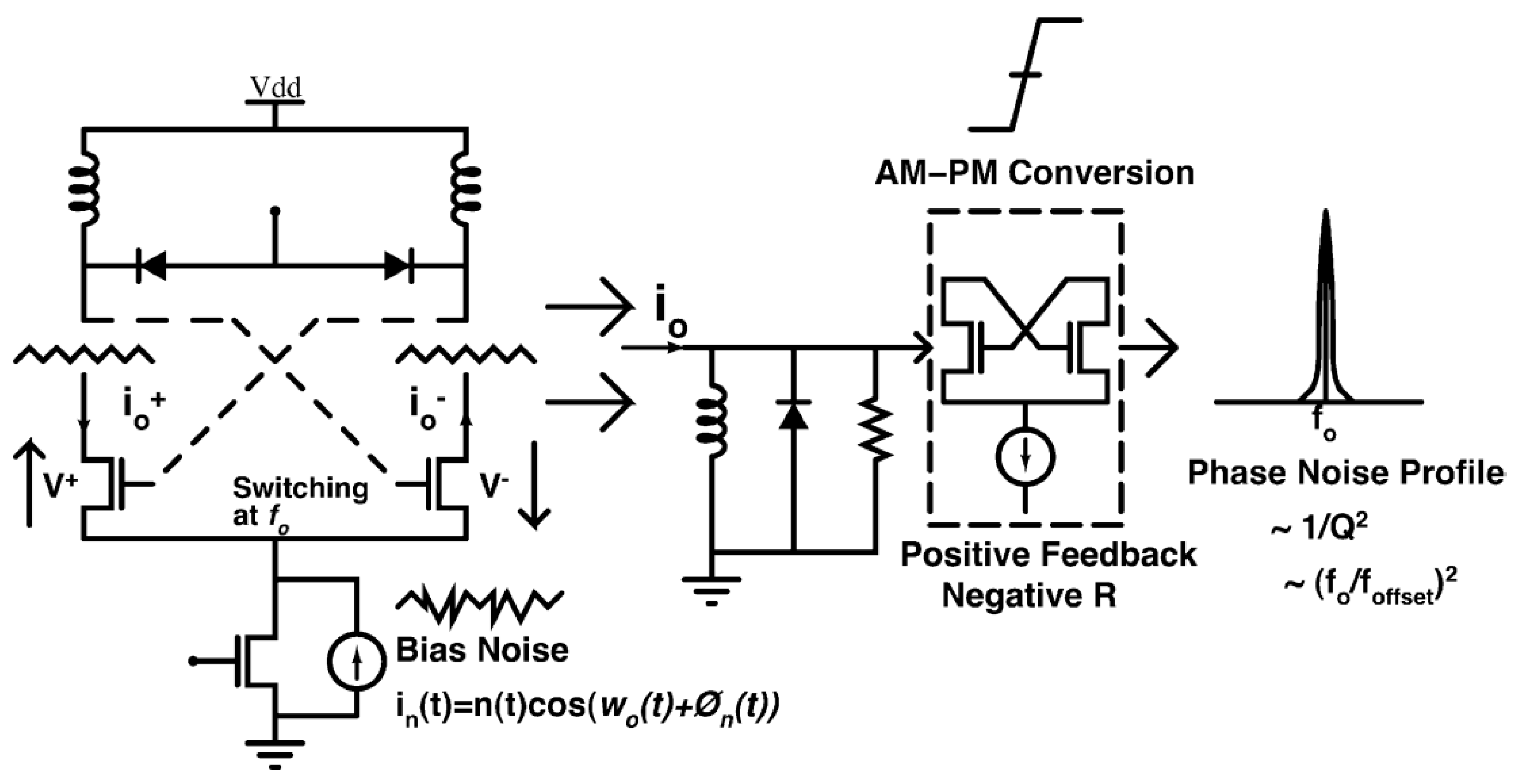
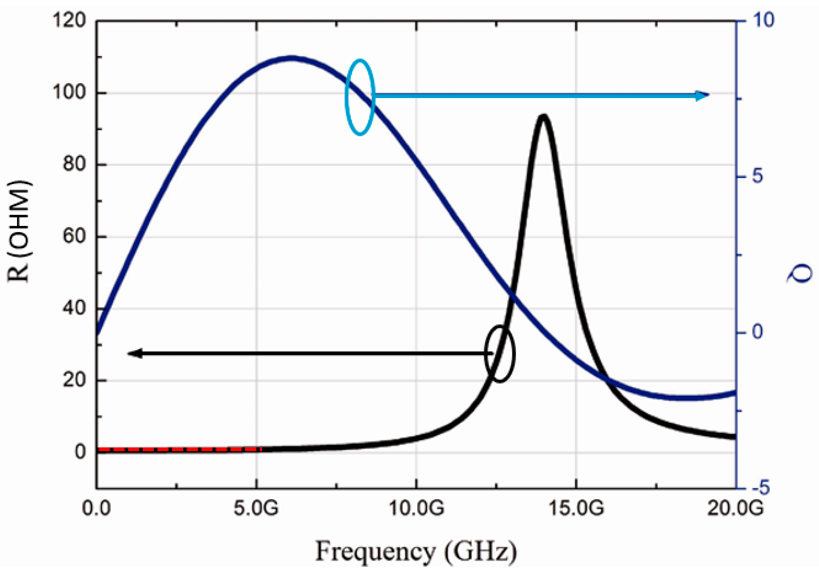
2.1. Phase Noise
2.2. Buffer Circuit and Optimization
3. Simulation and Measurement Results
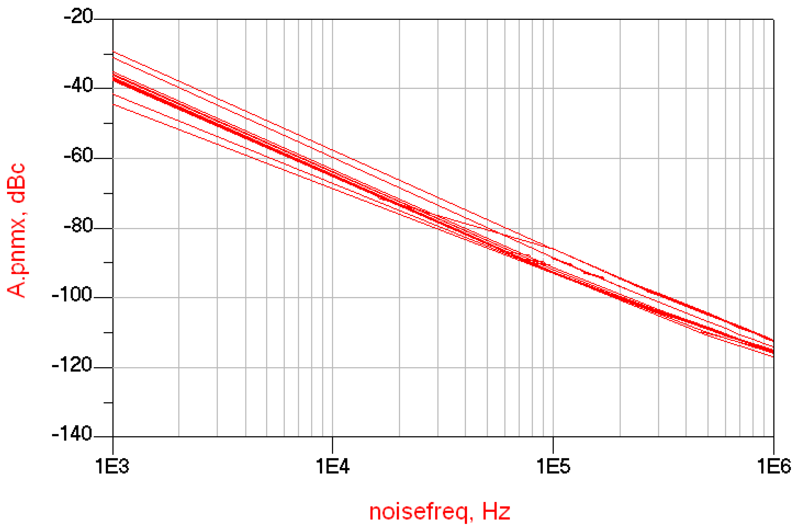
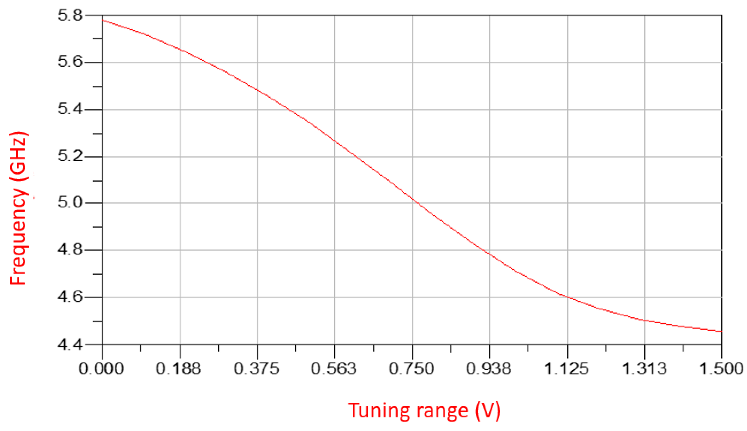
3.1. Simulation Results
- First, the application specifications must be developed.
- The design is to be simulated using ADS software (Advanced Design System, Keysight Technologies, version 2019) to determine if the specifications can be met by the circuit architecture.
- The layout is designed using the Virtuoso layout editor. The caliber is used for the verification of DRC and LVS.
- The layout file is reloaded into ADS. It is recommended that an EM simulation is performed using ADS. This is to extract whether the circuit conforms to the specification after realization.
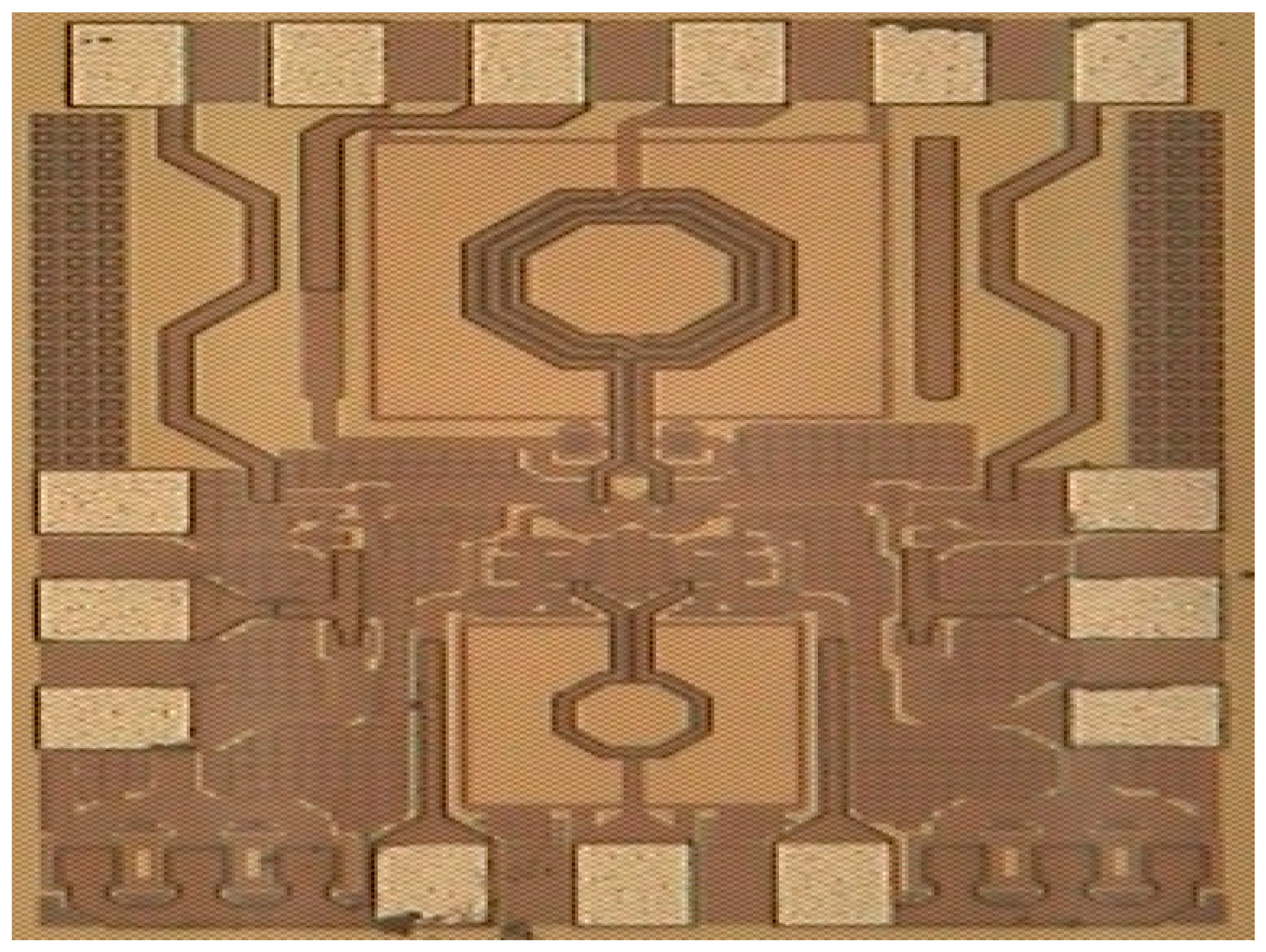
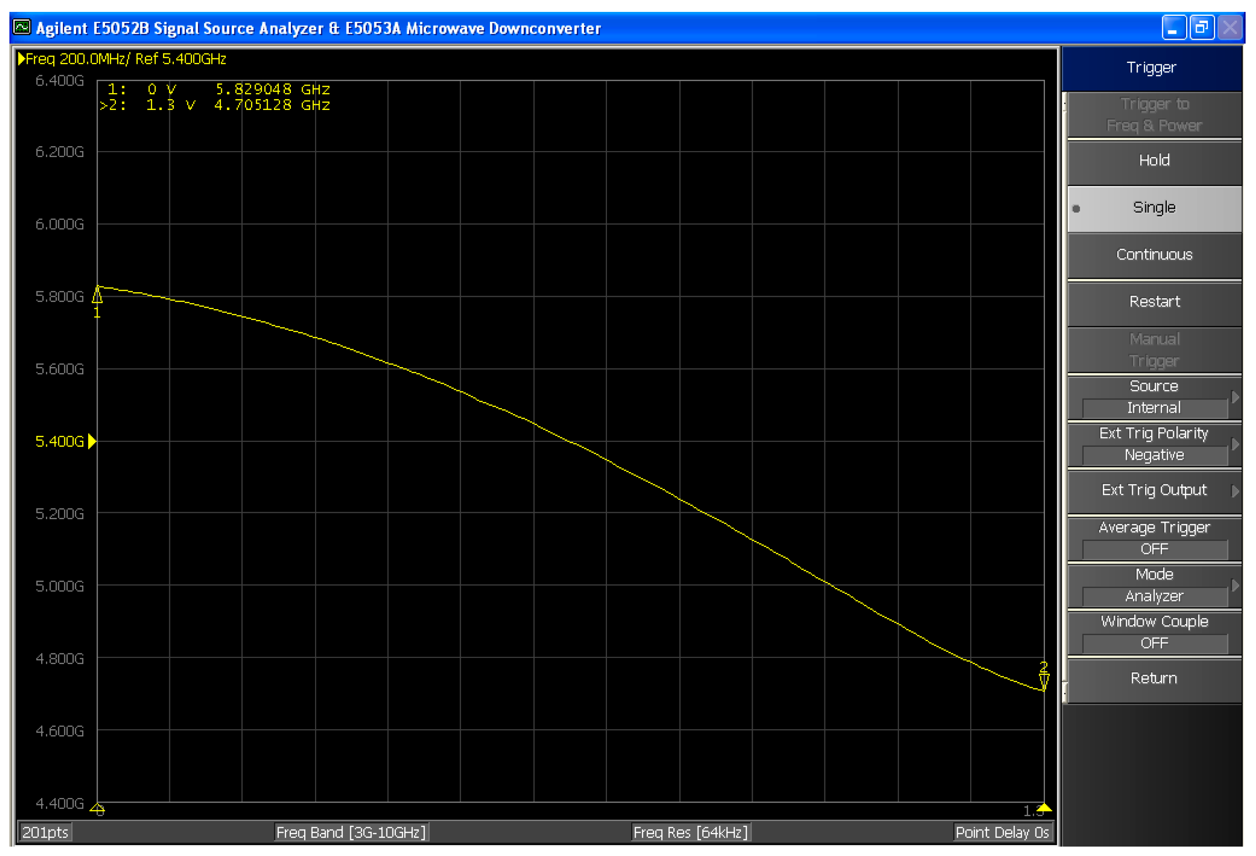
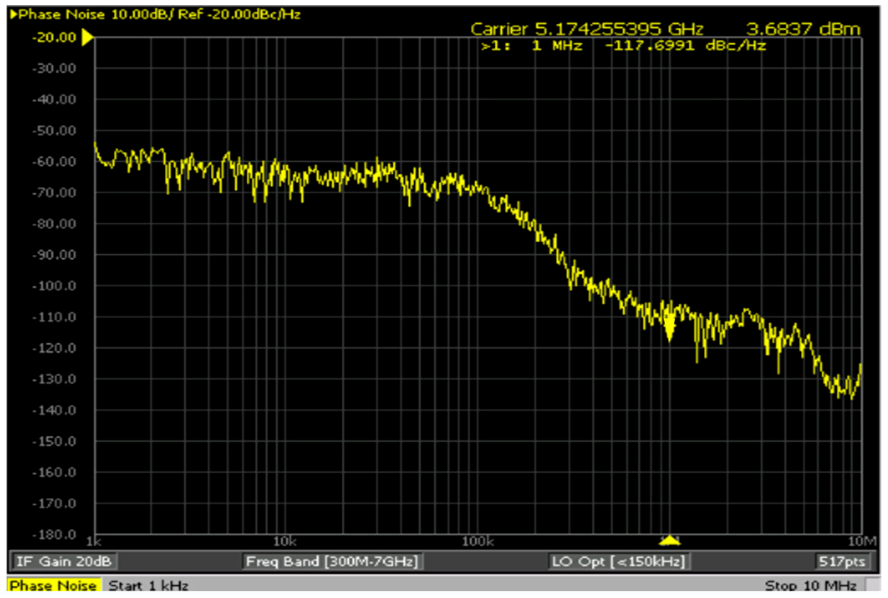
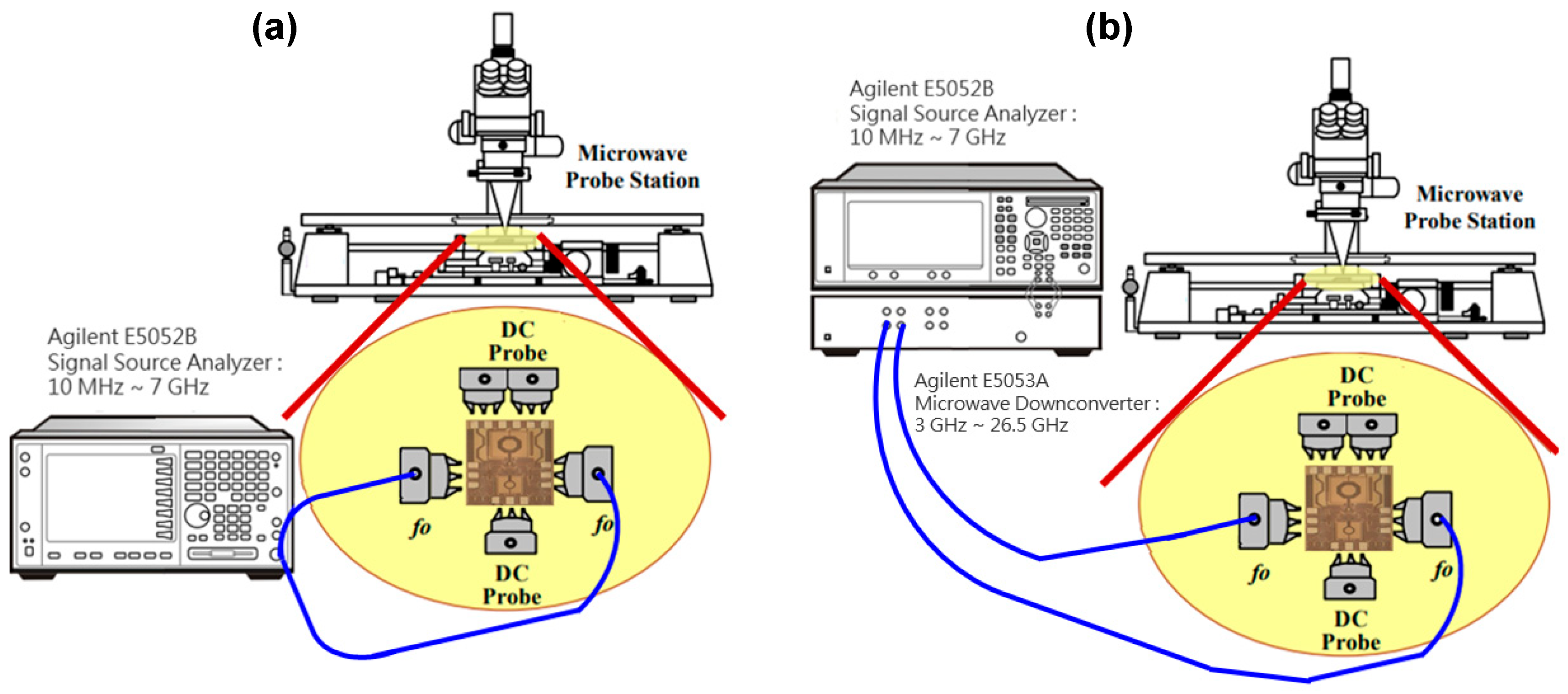
3.2. Measurement Results
- -
- L(Δf) is the phase noise at offset Δf.
- -
- f0 is the oscillation frequency (in Hz).
- -
- PDC is the power consumption (in mW).
- -
- TR is the tuning range (%).
- -
- T is temperature (in Kelvin), which is taken as 300 K in this work.
- -
- TR is the tuning range and k is Boltzmann’s constant. A temperature of 300 K is used for the PFTN calculation.
4. Conclusions
Author Contributions
Funding
Data Availability Statement
Conflicts of Interest
References
- Singh, S.; Arya, R.K.; Sahana, B.C. RF Circuits for 5G Applications: Designing with mmWave Circuitry, 1st ed.; John Wiley & Sons: Hoboken, NJ, USA, 2023. [Google Scholar]
- Sobot, R. Wireless Communication Electronics: Introduction to RF Circuits and Design Technique, 2nd ed.; Springer: Cham, Switzerland, 2021. [Google Scholar]
- Free, C.E.; Aitchison, C.S. RF and Microwave Circuit Design: Theory and Applications, 1st ed.; John Wiley & Sons: Hoboken, NJ, USA, 2021. [Google Scholar]
- De Cock, W.; Steyaert, M.A. CMOS 10GHz voltage controlled, LC-oscillator with integrated high-Q inductor. In Proceedings of the 27th European Solid-State Circuits Conference, Villach, Austria, 18–20 September 2001; pp. 498–501. [Google Scholar]
- Hung, C.M.; Shi, L.; Lagnado, I.; O, K.K. A 25.9-GHz Voltage-controlled oscillator fabricated in a CMOS process. In Proceedings of the 2000 Symposium on VLSI Circuits. Digest of Technical Papers (Cat. No.00CH37103), Honolulu, HI, USA, 15–17 June 2000; pp. 100–101. [Google Scholar]
- Razavi, B. Design of Analog CMOS Integrated Circuits, 2nd ed.; McGraw-Hill Education: New York, NY, USA, 2017. [Google Scholar]
- Lesson, D.B. A simple model of feedback oscillator noise spectrum. Proc. IEEE 1966, 54, 329–330. [Google Scholar] [CrossRef]
- Hajimiri, A.; Lee, T.H. A general theory of phase noise in electrical oscillators. IEEE J. Solid-State Circuits 1998, 33, 179–194. [Google Scholar] [CrossRef]
- Hajimiri, A.; Lee, T.H. Design Issuse in CMOS Differential LC Oscillators. IEEE J. Solid-State Circuits 1999, 34, 717–724. [Google Scholar] [CrossRef]
- Hajimiri, A.; Lee, T.H. Oscillator Phase Noise: A Tutorial. IEEE J. Solid-State Circuits 2000, 35, 326–335. [Google Scholar]
- Jerng, A.; Sodini, C.G. The impact of device type and sizing on phase noise mechanisms. IEEE J. Solid-State Circuits 2005, 40, 360–369. [Google Scholar] [CrossRef]
- Perraud, L.; Bonnot, L.; Sornin, N.; Pinatel, C. Fully Integrated 10 GHz CMOS VCO for Multi-Band WLAN Applications. In Proceedings of the 29th European Solid-State Circuits Conference (ESSCIRC), Estoril, Portugal, 16–18 September 2003; pp. 353–356. [Google Scholar]
- Tiebout, M. Low-power low-phase-noise differentially tuned quadrature VCO design in standard CMOS. IEEE J. Solid-State Circuits 2001, 36, 1018–1024. [Google Scholar] [CrossRef]
- Liu, J.; Liao, H.; Huang, R. A 5-GHz low-phase noise CMOS VCO with swing boosting technique. Microw. Opt. Technol. Lett. 2009, 51, 2061–2064. [Google Scholar] [CrossRef]
- Lo, Y.-C.; Silva-Martinez, J. A 5-GHz CMOS LC quadrature VCO with dynamic current-clipping coupling to improve phase noise and phase accuracy. IEEE Trans. Microw. Theory Tech. 2013, 61, 2632–2640. [Google Scholar] [CrossRef]
- Moon, Y.J.; Roh, Y.-S.; Jeong, C.-Y.; Yoo, C. A 4.39-5.26 GHz LC-Tank CMOS voltage controlled oscillator with small VCO-gain variation. IEEE Microw. Wirel. Compon. Lett. 2009, 19, 524–526. [Google Scholar] [CrossRef]


| Post-Simulation | Measurement | |
|---|---|---|
| Frequency (GHz) | 5 | 5.06 |
| Tuning Range (MHz) | 1324 | 1124 |
| Phase Noise (dBc/Hz) | −116.5 | −117.69 |
| FOM (dBc/Hz @ MHz) | −181.4 | −196.6 |
| Output Power (dBm) | −4.6 | −22.44 |
| Power Consumption (mW) | 8.1 | 3.4 |
| Chip Size (mm2) | 0.499 | |
| Ref. | CMOS Tech. (μm) | Frequency (GHz) | Phase Noise, dBc/Hz @ 1 MHz | Tuning Range (%) | FOM (dBc/Hz) | PDC (mW) | PFTN (dB) |
|---|---|---|---|---|---|---|---|
| [11] | 0.18 | 5.3 | −124 | 8 | −190 | 13.5 | −9.09 |
| [14] | 0.18 | 5 | −122.7 | 6.4 | −189.3 | 5.28 | −8.25 |
| [15] | 0.13 | 5 | −121 | 20 | −189 | 4.2 | N/A |
| [16] | 0.18 | 5.2 | −113.7 | 9.56 | −180 | 9.7 | N/A |
| This work | 0.18 | 5.06 | −117.7 | 22.2 | −188.6 | 3.4 | −4.3 |
Disclaimer/Publisher’s Note: The statements, opinions and data contained in all publications are solely those of the individual author(s) and contributor(s) and not of MDPI and/or the editor(s). MDPI and/or the editor(s) disclaim responsibility for any injury to people or property resulting from any ideas, methods, instructions or products referred to in the content. |
© 2025 by the authors. Licensee MDPI, Basel, Switzerland. This article is an open access article distributed under the terms and conditions of the Creative Commons Attribution (CC BY) license (https://creativecommons.org/licenses/by/4.0/).
Share and Cite
Hsu, J.-J.; Lin, Y.-C.; Yang, S.J.H. A 0.8 V Low-Power Wide-Tuning-Range CMOS VCO for 802.11ac and IoT C-Band Applications. J. Low Power Electron. Appl. 2025, 15, 32. https://doi.org/10.3390/jlpea15020032
Hsu J-J, Lin Y-C, Yang SJH. A 0.8 V Low-Power Wide-Tuning-Range CMOS VCO for 802.11ac and IoT C-Band Applications. Journal of Low Power Electronics and Applications. 2025; 15(2):32. https://doi.org/10.3390/jlpea15020032
Chicago/Turabian StyleHsu, Jung-Jen, Yao-Chian Lin, and Stephen J. H. Yang. 2025. "A 0.8 V Low-Power Wide-Tuning-Range CMOS VCO for 802.11ac and IoT C-Band Applications" Journal of Low Power Electronics and Applications 15, no. 2: 32. https://doi.org/10.3390/jlpea15020032
APA StyleHsu, J.-J., Lin, Y.-C., & Yang, S. J. H. (2025). A 0.8 V Low-Power Wide-Tuning-Range CMOS VCO for 802.11ac and IoT C-Band Applications. Journal of Low Power Electronics and Applications, 15(2), 32. https://doi.org/10.3390/jlpea15020032