Article

Design and Analysis of an Ultra-Wideband High-Precision Active Phase Shifter in 0.18 μm SiGe BiCMOS Technology

1
The 13th Research Institute, China Electronics Technology Group Corporation, Shijiazhuang 050051, China
2
School of Microelectronics, Tianjin University, Tianjin 300072, China
*
Author to whom correspondence should be addressed.
J. Low Power Electron. Appl. 2025, 15(2), 30; https://doi.org/10.3390/jlpea15020030
Submission received: 29 March 2025 / Revised: 3 May 2025 / Accepted: 6 May 2025 / Published: 7 May 2025
(This article belongs to the Topic Advanced Integrated Circuit Design and Application)

Abstract

:
This paper presents an active phase shifter for phased array system applications, implemented using 0.18 μm SiGe BiCMOS technology. The phase shifter circuit consists of a wideband quadrature signal generator, a vector modulator, an input balun, and an output balun. To enhance the bandwidth, a polyphase filter is employed as the quadrature signal generator, and a two-stage RC-CR filter with a highly symmetrical miniaturized layout is cascaded to create multiple resonant points, thus extending the phase shifter’s bandwidth to cover the required range. The gain of the variable-gain amplifier within the vector modulator is adjustable by varying the tail current, thereby enlarging the range of selectable points, improving phase-shifting accuracy, and reducing gain fluctuations. The measurement results show that the proposed active phase shifter achieves an RMS phase error of less than 2° and a gain variation ranging from −1.2 dB to 0.1 dB across a 20 GHz to 30 GHz bandwidth at room temperature. The total chip area is 0.4 mm2, with a core area of 0.165 mm2, and consumes 19.5 mW of power from a 2.5 V supply.

1. Introduction

Phased array systems are a key technology in wireless communication, utilizing beamforming and beam-shaping techniques. These systems consist of multiple antenna elements that can independently adjust the phase and amplitude of signals, enabling precise control over the direction of transmission or reception [1]. In communication applications, phased arrays enable high-speed wireless data transmission and multi-user access, offering enhanced network capacity and improved link reliability. Phased arrays also play a critical role in high-resolution target detection and tracking, providing accurate spatial localization. Moreover, they have broad applications in fields such as radio antennas, aerospace communications, and millimeter-wave imaging systems [2].
In phased array systems, the phase shifter is one of the key components, as it adjusts the phase differences between antenna elements according to the desired beam direction and shape. This adjustment allows for coherent signal addition, enabling beam steering and focusing. The resolution and phase accuracy of the phase shifter directly influence the beam resolution and width in beamforming. As a result, there are increasingly stringent requirements for phase shifters in terms of insertion loss, accuracy, bandwidth, and chip area for phased array system applications [3]. Phase shifters can generally be categorized into passive and active types. Passive phase shifters, such as switch-type phase shifters (STPSs) [4,5,6], reflection-type phase shifters (RTPSs) [7,8,9], and hybrid passive implementations [10,11,12], offer excellent linearity and consume no static power. However, they are often constrained by limited phase resolution, a restricted phase tuning range, increased insertion loss, and a large chip area. In contrast, vector-modulated active phase shifters [13,14,15] demonstrate superior characteristics, including high resolution, low loss, and compact integration. Among the various technology platforms, silicon–germanium (SiGe) BiCMOS has emerged as a highly attractive solution for 5G transceiver design. Compared to CMOS and III-V technologies, SiGe offers a balanced trade-off among cost efficiency, integration density, noise performance, and output power capability. Recent developments in SiGe-based phased array architectures have validated the feasibility of implementing compact, multi-channel RF beamforming systems for 5G applications, as reported in several contemporary studies [16,17].
This paper presents an ultra-wideband active phase shifter operating in the K and Ka bands, tailored for phased array systems. The proposed phase shifter features an innovative variable tail current approach. By modifying the tail current of the variable-gain amplifier (VGA), the range of selectable phase points is extended, leading to improved phase shifting accuracy and reduced gain fluctuations.

2. Analysis and Design of the Active Phase Shifter Circuit

As outlined in the basic principles of phased array systems [18,19], the phase shifter plays a crucial role in the overall system, which imposes stringent requirements on parameters such as phase shifting accuracy and amplitude fluctuations. To maintain high phase accuracy and low amplitude variation across a wide frequency band, this paper presents the design of an active phase shifter tailored for phased array system applications.

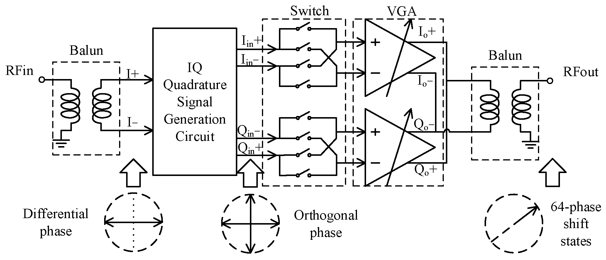
2.1. Circuit Architecture

Figure 1 shows the basic structure of the proposed phase shifter. The single-ended RF input signal is first converted into a differential signal by the input balun, which then enters the quadrature signal generator to produce four orthogonal IQ signals. To achieve wideband performance while maintaining good orthogonality, the quadrature signal generation circuit utilizes a second-order RC-CR network structure. This design sacrifices insertion loss to expand the operating bandwidth. The four IQ signals generated by the quadrature signal generator are fed into the variable-gain amplifier (VGA). The VGA adopts a common-source configuration, and the four output signals are directly combined into two differential signals. Finally, the desired 64-state phase-shifted signals are obtained through the output balun.

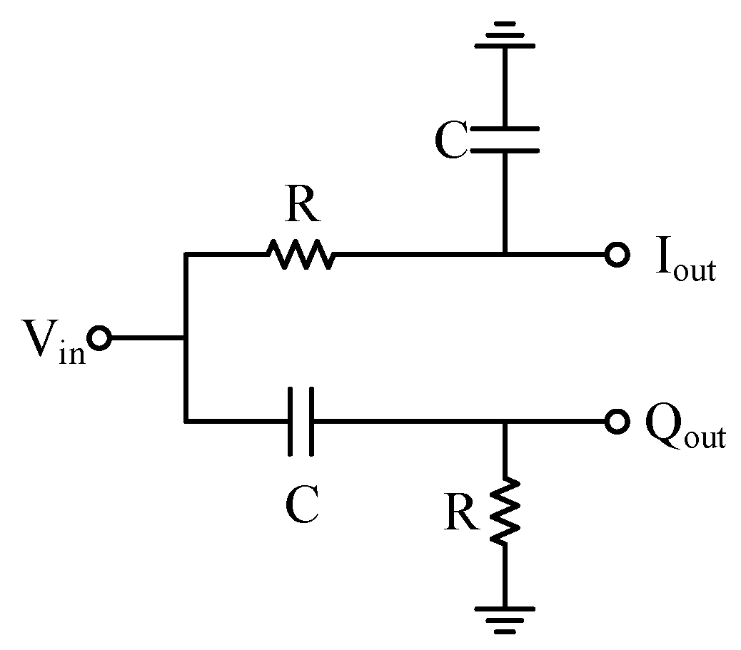
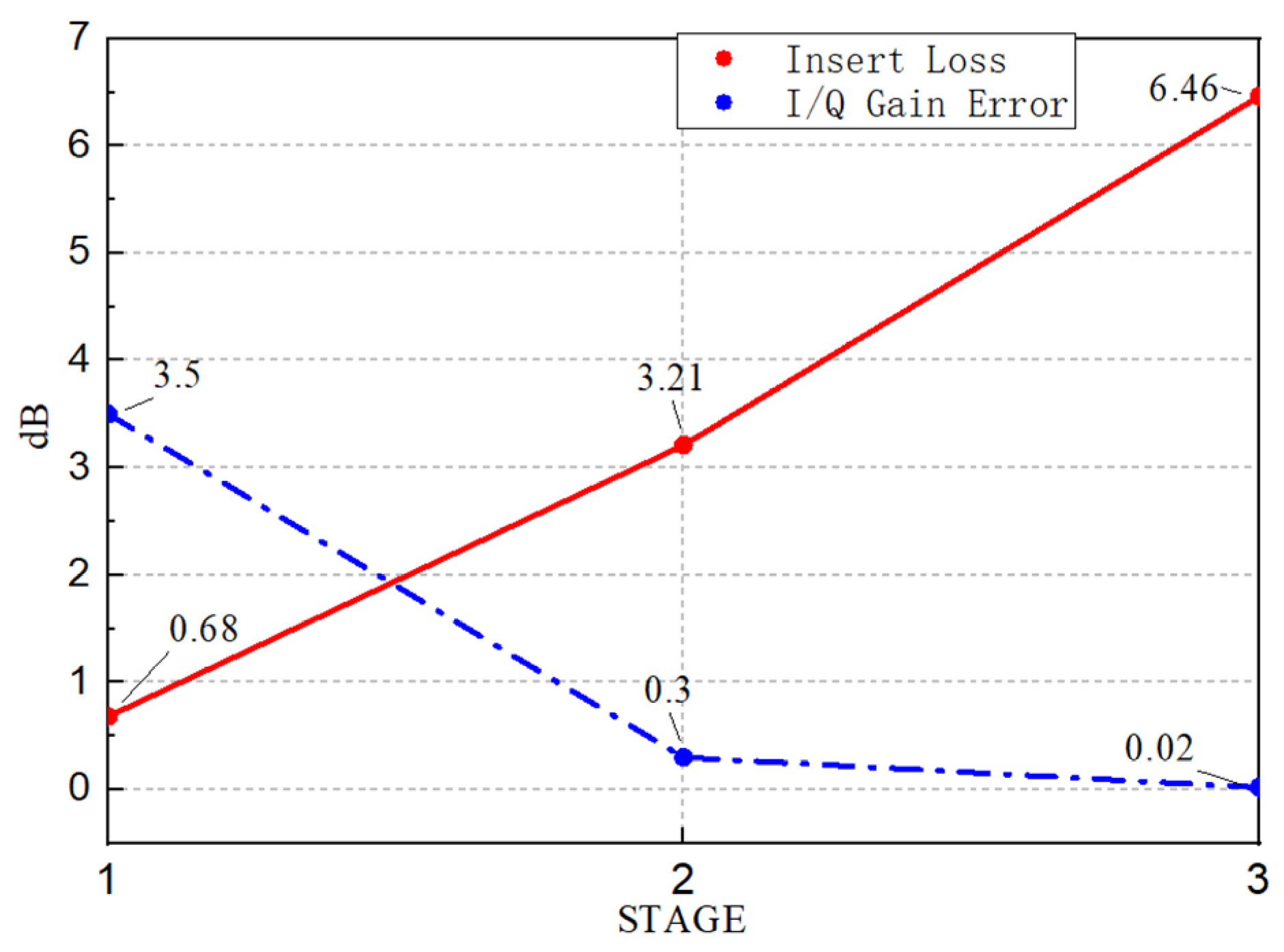
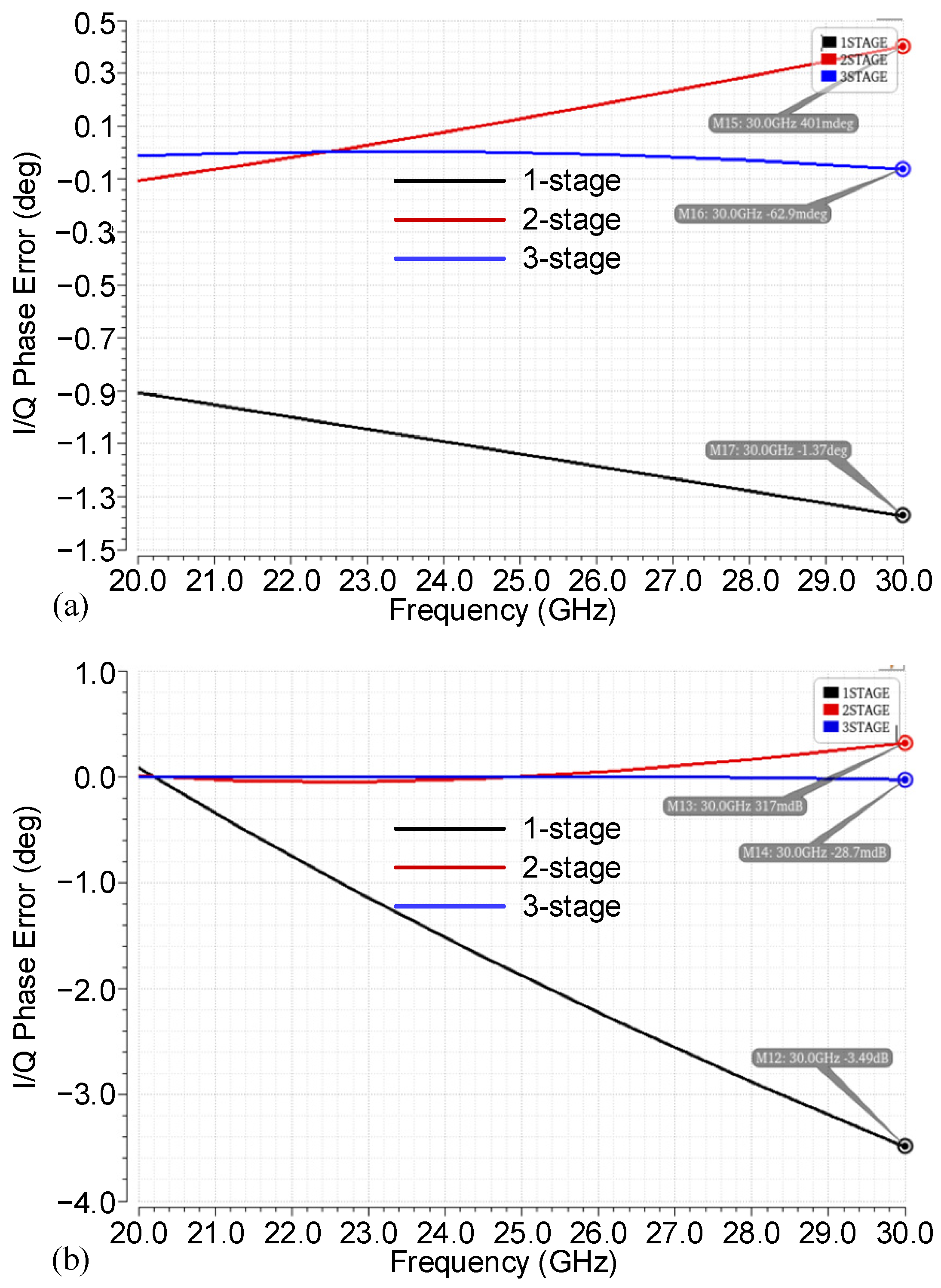
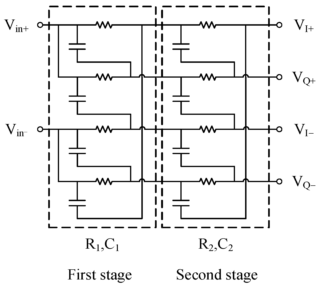
2.2. Quadrature Signal Generation Circuit Design

The quadrature signal generation circuit in this paper employs an RC-CR frequency-selective network. The traditional quadrature signal generator based on an RC-CR network is shown in Figure 2. This circuit consists of an RC low-pass filter and a CR high-pass filter, which produces output signals Iout and Qout with a 90° phase difference. When the angular frequency ω = 1/RC, the magnitudes of the output signals Iout and Qout are equal. However, as the signal bandwidth increases, the orthogonality of the output signals degrades. Therefore, a single-stage RC-CR quadrature signal generator is typically used in narrowband systems [20].
To expand the bandwidth, this paper adopts a cascaded configuration of the single-stage RC-CR network. By introducing multiple poles, this approach extends the bandwidth while making the structure less sensitive to the load capacitance at the output. The more stages added to the RC-CR network, the wider the covered bandwidth becomes, but at the cost of increased insertion loss [21]. Figure 3 shows the insertion loss and amplitude error of the RC-CR network vary with the number of its stages. Figure 4 shows the simulation results of phase error and amplitude error. Considering the design requirements for bandwidth, insertion loss, and phase shifting error, a two-stage cascaded polyphase filter structure was ultimately selected.
Figure 5 illustrates the two-stage polyphase filter obtained by cascading RC-CR networks. This polyphase filter has two orthogonal frequency points: ω1 = 1/R1C1 and ω2 = 1/R2C2. When the resistor and capacitor values are appropriately chosen, the orthogonality of the output signals is optimized. To cover the 20 GHz to 30 GHz bandwidth, the two poles of the cascaded polyphase filter are positioned at 20 GHz and 25 GHz, respectively, thereby covering the entire frequency range.
Figure 6 shows the layout of the proposed highly symmetrical miniaturized two-stage RC-CR polyphase filter. Compared with traditional quadrature signal generation modules, RC-CR networks have a small natural area and can expand the bandwidth through multi-stage cascade to realize broadband application. The second-order RC-CR network in this paper further reduces the layout area through highly symmetrical miniaturized layout and makes the length of each signal path equal as much as possible to reduce the amplitude and phase errors caused by the layout.
In the design and pre-simulation of the polyphase filter, resistors and capacitors in series were used as the equivalent load impedance for the subsequent variable-gain amplifier (VGA). The simulation results demonstrate that the two-stage polyphase filter exhibits excellent orthogonality, with a phase difference of 90.13° between the two output signals at 25 GHz, which is very close to the ideal value. The filter also resonates at approximately 20 GHz and 25 GHz, with the maximum amplitude error within the bandwidth being only 0.3 dB.

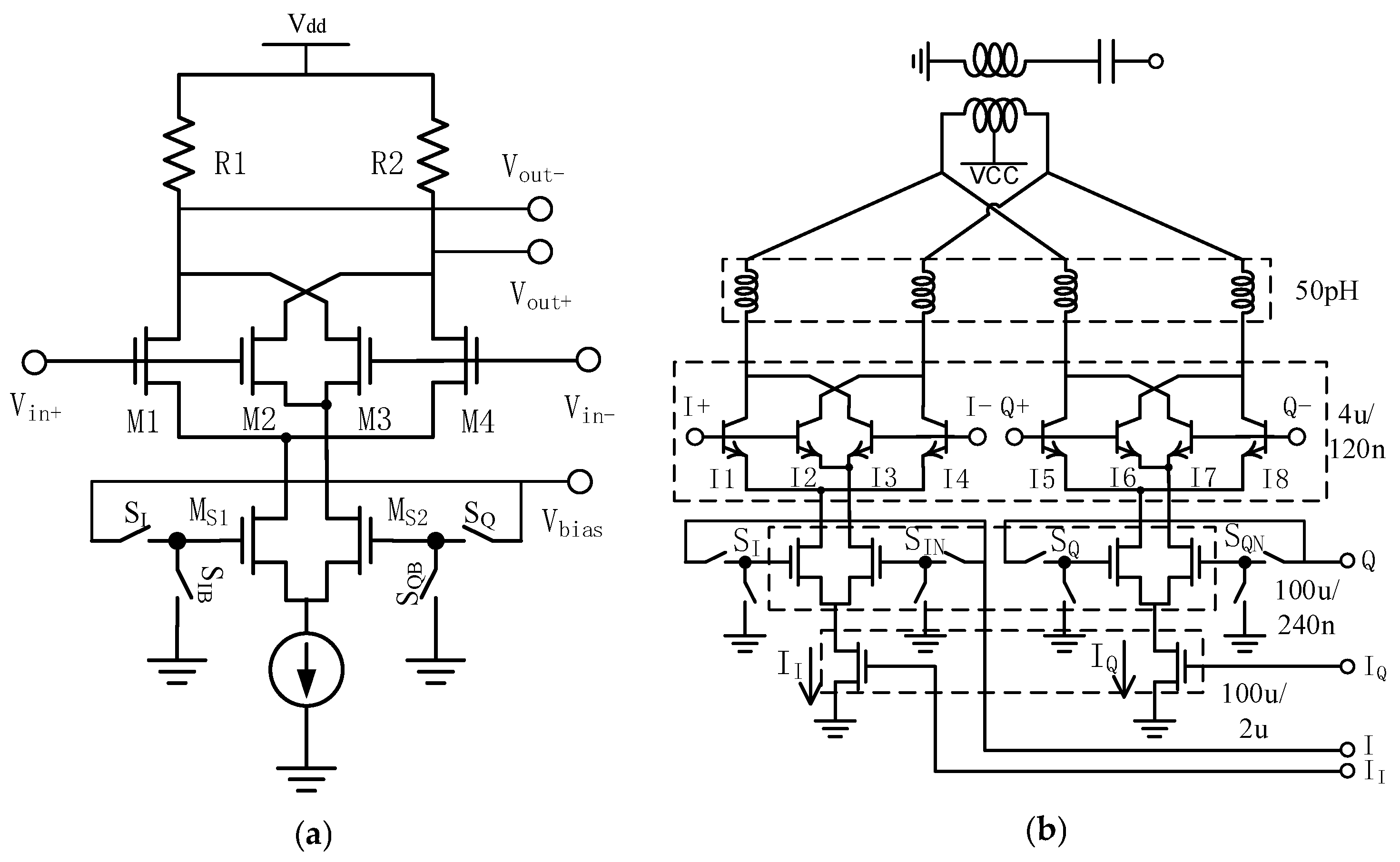
2.3. Vector Modulator Design

The vector modulator designed in this paper consists of two sets of variable-gain amplifiers (VGAs), each responsible for modulating the four orthogonal signals generated by the preceding quadrature signal generator. The output signals are then combined to produce two differential signals. The phase of the output differential signals depends on the relative amplitudes of the orthogonal signals. The VGA circuits used in this design are Gilbert cells with switch control, as shown in Figure 7a. In the Gilbert cell configuration, transistors M1 and M4 and transistors M2 and M3 form two differential amplifiers. The control signals SI and SIB are oppositely phased switches. When switch SI is on and switch SIB is off, the differential amplifier formed by M1 and M4 operates normally, while the amplifier formed by M2 and M3 is turned off. Conversely, when SIB is on and SI is off, the differential amplifier formed by M2 and M3 operates, while the amplifier formed by M1 and M4 is turned off. At any given time, only one differential amplifier is active, and the phase difference between the two output signals is 180°.
The vector modulator designed in this paper consists of two sets of Gilbert cells with switch control, as shown in Figure 7b. The set of transistors I1–I4 forms one VGA, and I5–I8 forms another. As previously analyzed, the switches SI, SIN, SQ, and SQN control the activation and deactivation of the four differential amplifiers in the two VGAs, ensuring that only one differential amplifier from each VGA is active at any given time. Additionally, the phase difference between the output signals of a single VGA in its two switching states is 180°. For example, consider the VGA formed by I1–I4. The differential signals I+ and I are the input signals from the quadrature signal generator, which serve as inputs to the VGA. By controlling the tail current II, the gain of the differential amplifier is adjusted, which in turn changes the amplitude of the output signal. Similarly, the input signals Q+ and Q for the second VGA, formed by I5–I8, control the output signal amplitude by adjusting the tail current IQ. The output signals from the two VGAs are then combined at the output, where a balun is used to sum the I and Q paths. The inductors in the four branches perform impedance matching. The switches SI, SIN, SQ, and SQN control the combination of the four quadrature signals, producing four distinct output states, corresponding to the four quadrants of the constellation diagram [22]. The switching signal is controlled by the on-chip Serial Peripheral Interface (SPI), and the relationship between the corresponding quadrant and the switching signal is shown in Table 1.
The output phase shift of the phase shifter is determined by the ratio of the tail currents II and IQ in in the Gilbert cells. To minimize amplitude fluctuations in the phase shift, it is essential to maintain a constant gain in the vector modulator. Thus, the sum of the tail currents for the two sets of Gilbert cells must remain constant. To improve phase shifting accuracy, a six-bit gate voltage control circuit is used to provide the gate voltage for the tail current transistors. The six-bit gate voltage is also produced by the on-chip SPI. It controls the quadrature signal synthesis of adjacent quadrants to obtain different phase offsets, and the multi-bit high-precision control voltage can make the phase precision of vector synthesis higher. The configuration allows for 64 distinct states in each quadrant, with two-bit control codewords used to manage the four quadrant states. In total, 256 distinct phase states are achievable, with ideal conditions ensuring that the state points are evenly distributed on a circle. The final 64 states for phase shifting are selected from these 256 states. Electromagnetic simulations of the phase shifter were performed, and after scanning all states, the best 64 states were selected using simulation software (Advanced Design System 2019). The resulting constellation diagram and the RMS phase error for the phase shifter are shown in Figure 8 and Figure 9, respectively.

2.4. Amplitude Fluctuation Mitigation Technique

As analyzed earlier, in the ideal case, the 256 states form a perfect circle, which allows for optimal phase shifting accuracy and amplitude fluctuation performance. However, the relationship between current and gain is non-linear, which distorts the resulting circle and ultimately degrades both phase shifting accuracy and amplitude fluctuation performance. The simulated results for phase shifting gain fluctuation, obtained earlier, are shown in Figure 10. From the figure, it can be observed that the gain fluctuation is ±1 dB, indicating poor gain consistency.
This paper proposes an innovative solution by improving the bias current generation circuit of the VGA to mitigate the aforementioned impact. Multiple bias current states are introduced to increase the number of phase states at the output. This approach enhances the margin of selectable phase states, ensuring that the selected 64-phase states are distributed more uniformly, forming a nearly ideal circle. As a result, the phase shifting accuracy is improved, and the amplitude fluctuations are reduced.
The specific design approach is as follows: Figure 11 shows the reference current generation circuit. Prior to the improvement, it could only output a fixed reference current IB. In the improved design, two additional mirror current paths are added to supplement the output current, with the replication ratio adjustable to ensure that the newly introduced currents remain within a reasonable range. In this design, the base reference current is set to 5 µA, the first supplementary current is 0.5 µA, and the second supplementary current is 1 µA. The supplementary current paths are controlled by switches driven by two-bit control codes, which allow for three selectable current values: 5 µA, 5.5 µA, and 6 µA.
The PTAT (positive temperature coefficient of absolute temperature) current generated by the reference current generation circuit flows into the gate voltage control circuit. By using a current replication technique in a certain proportion, six branch currents for the gate voltage control circuit are generated. Each branch is controlled by switches, ensuring that the current flows into only one of the I/Q control paths. This logic guarantees that the sum of the tail currents for the two sets of Gilbert cells remains constant. By altering the control code of the PTAT current, the sum of the tail currents for the two sets of Gilbert cells can be adjusted, thereby altering the gain of the differential amplifiers. This approach approximates the creation of three scaled circles, expanding the state points from 256 to 768. The increased number of selectable states allows the final 64-phase states to be more closely aligned with a perfect circle. Using the middle circle, which is controlled by a 5.5 µA current, as a reference, when the gain at a point on this circle is too low, a replacement can be found in the outer circle. Conversely, if the gain is too high, the inner circle can be used for replacements. This method helps maintain consistent gain, significantly improving phase shifting accuracy and reducing amplitude fluctuations.
Electromagnetic simulation tools were used to verify the proposed method of improving gain fluctuation by altering the tail current. Figure 12 shows the constellation diagram after increasing the number of state points by modifying the tail current. From the results, it is evident that the constellation diagram exhibits distinct circular groupings. After processing the results, the best 64-phase states are distributed within the three circles of state points. The gain fluctuation after reselecting the 64-phase states is shown in Figure 13, where the fluctuation is largely confined within a ±0.5 dB range. A comparison of phase accuracy RMS values for single-circle and three-circle configurations is presented in Figure 14, with the red line representing the single-circle result and the blue line representing the three-circle result. It is evident that the phase accuracy has significantly improved.

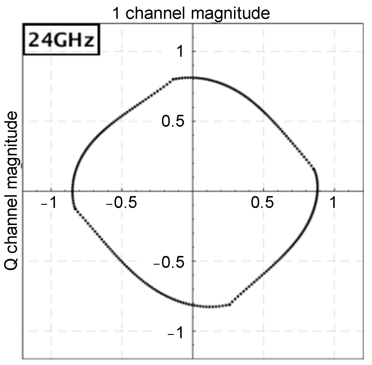
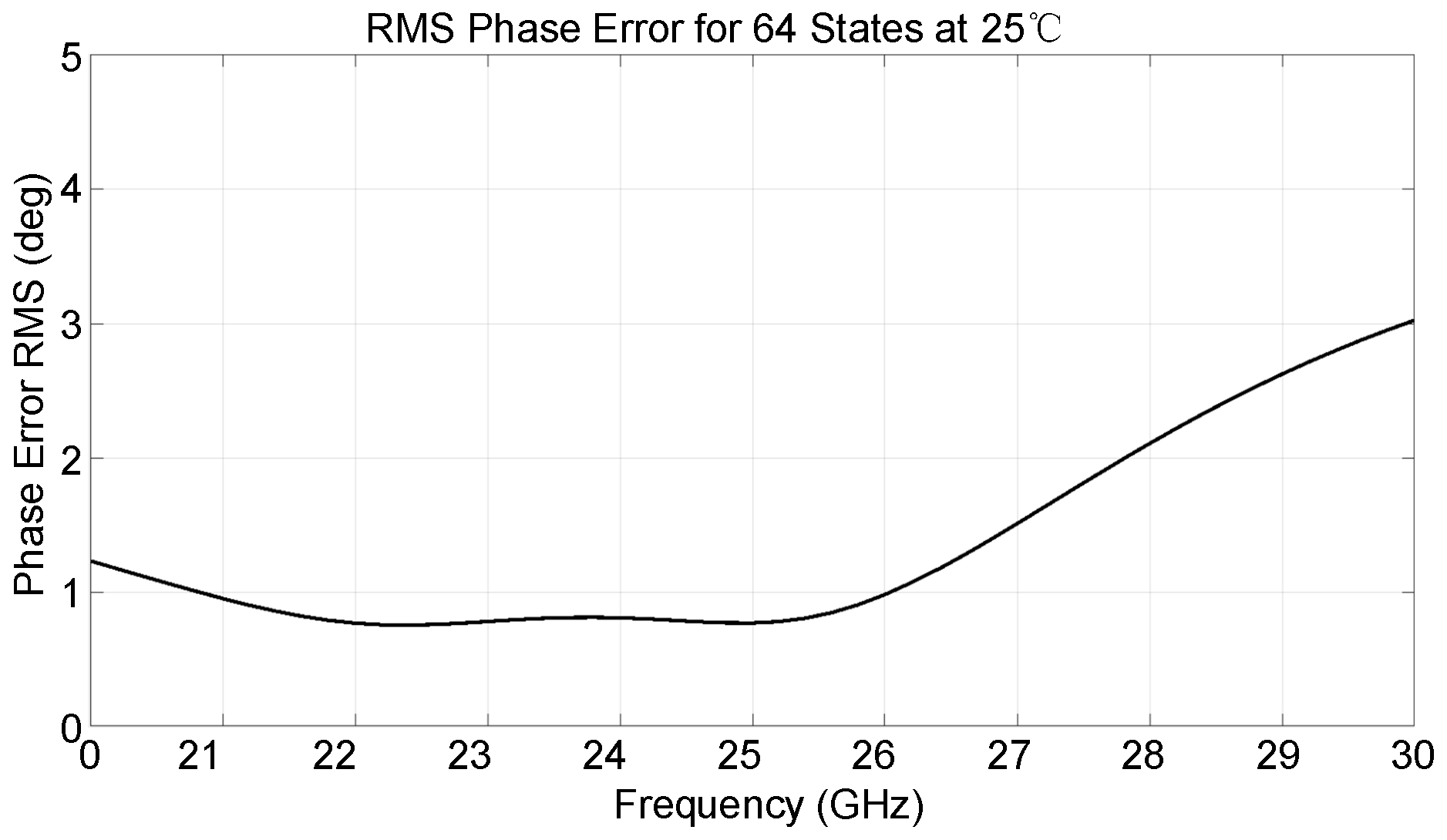
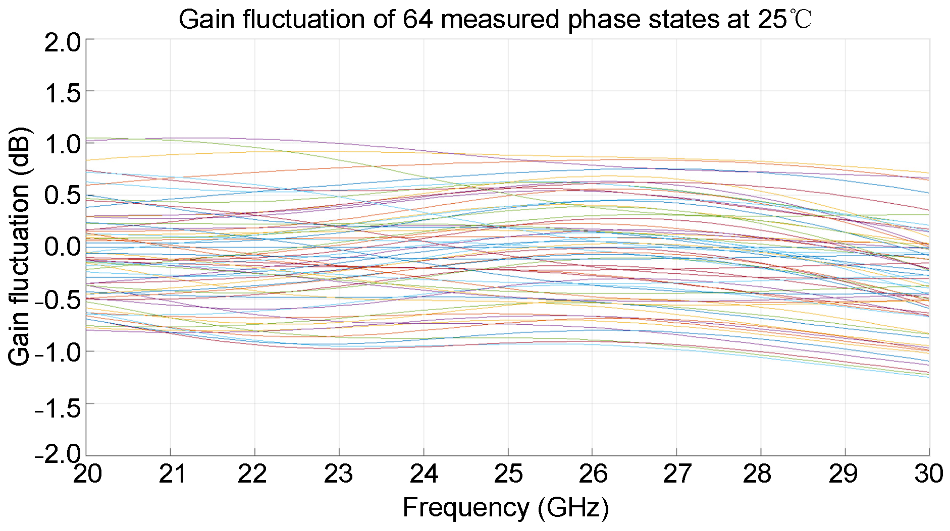
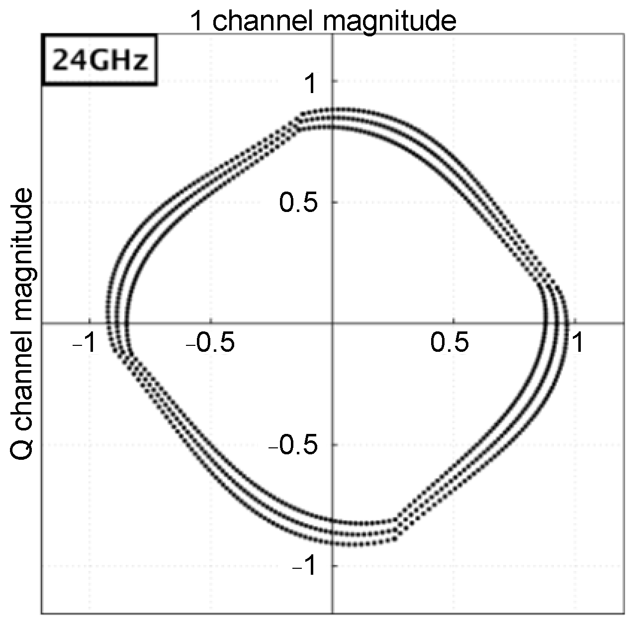
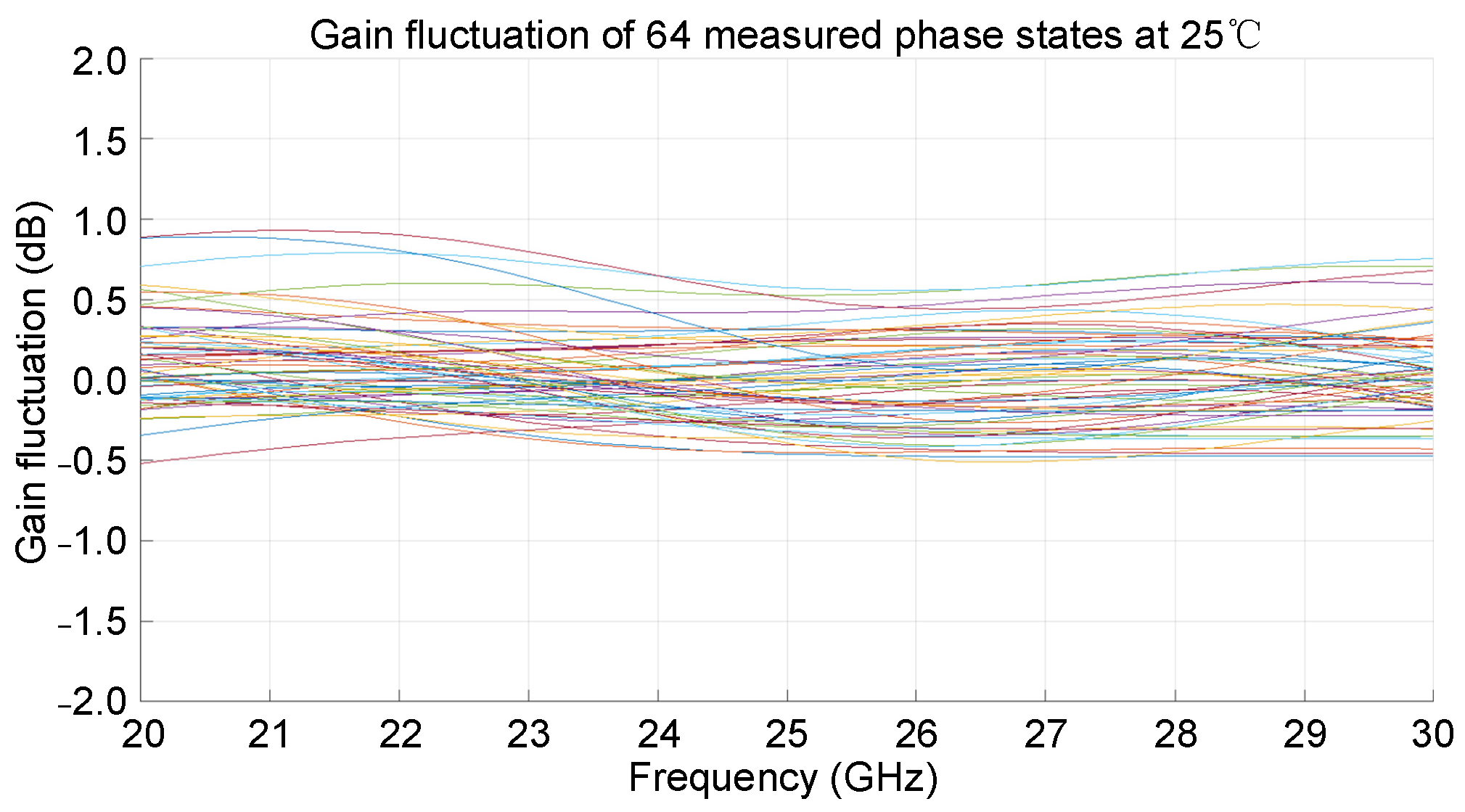
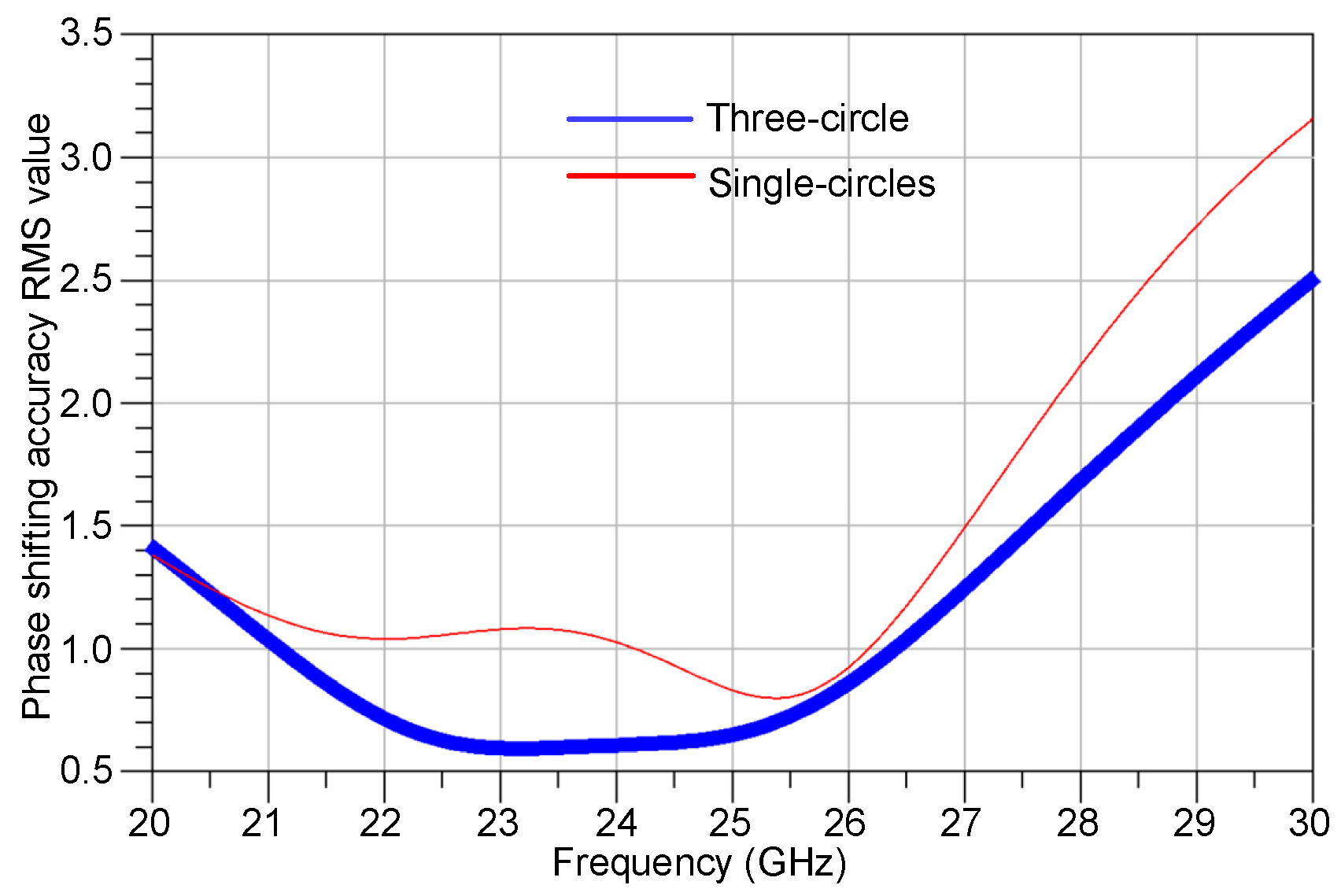
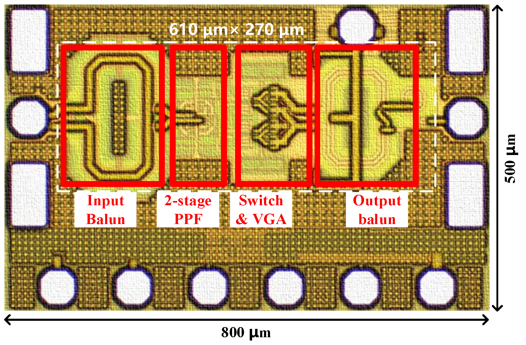
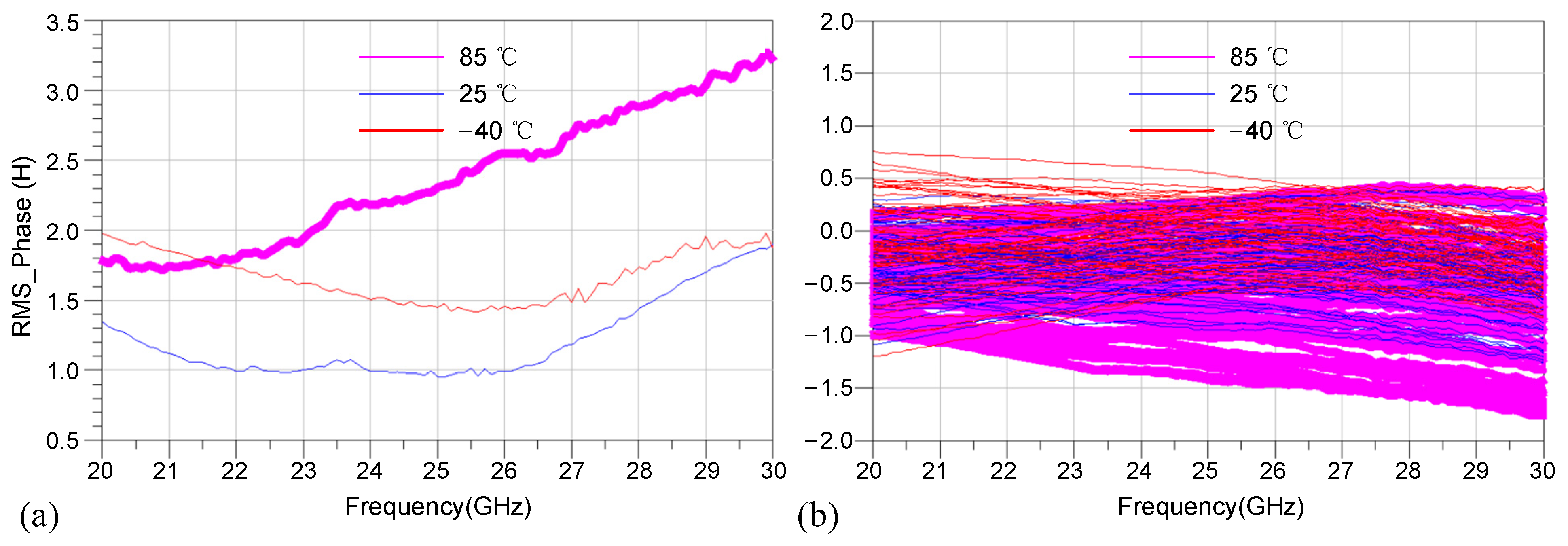
3. Measurement Results

Figure 15 shows a micrograph of the fabricated active phase shifter, implemented using a 0.18 μm SiGe BiCMOS process, with TSV (through-silicon via) used as the ground via. The overall chip size is 800 μm × 500 μm, with the core area measuring 610 μm × 270 μm. For chip testing, a GSG probe was used, and calibration was performed using the SOLT method. The power consumption of the whole circuit is 19.5 mW under a power supply of 2.5 V.
Figure 16 shows the phase shifting accuracy RMS value and gain fluctuation at room temperature (25 °C). Figure 17 presents the measured 64-QAM constellation diagram at room temperature. The active phase shifter designed in this paper achieves an RMS phase accuracy of less than 2° across the bandwidth range, with gain fluctuation ranging from −1.2 dB to 0.1 dB, demonstrating excellent phase shifting performance.
To evaluate the three-temperature performance of the active phase shifter, tests were conducted on the same chip, using the same phase control codes, at −40 °C, 25 °C, and 85 °C. Figure 18 shows the phase accuracy RMS values and gain fluctuations at the three temperatures, where red represents low temperature, blue represents room temperature, and pink represents high temperature. The test results indicate that, at both room temperature and low temperature, the RMS phase error remains below 2° across the frequency band, while at high temperature, the maximum phase error is slightly worse at 3.3°. The gain fluctuation across the three temperatures ranges from −1.7 dB to 0.7 dB.
To verify the inter-chip consistency, three chips were tested at room temperature, and the results for phase accuracy RMS and gain fluctuation are compared in Figure 19. The trends of the three chips are consistent, with the maximum RMS phase error being 0.3° and the gain fluctuation curves being tightly grouped. This demonstrates that the chip exhibits good inter-chip consistency.
Table 2 presents a performance comparison between the proposed phase shifter and other reported designs. Compared to existing studies, the prototype developed in this work demonstrates clear advantages in terms of area and power consumption, showcasing overall competitive performance.

4. Conclusions

This paper presents the design of an active vector synthesis phase shifter for phased array applications, implemented using a 0.18 μm SiGe BiCMOS process. The proposed phase shifter utilizes a two-stage RC-CR quadrature signal generation circuit to extend the bandwidth and reduces gain fluctuation while improving phase accuracy by varying the VGA tail current. The designed phase shifter covers a 360° phase shifting range from 20 GHz to 30 GHz, with a phase step size of 5.625°. The measured RMS phase accuracy remains below 3° across the temperature range of −40 °C to 85 °C, with gain fluctuation between −1.7 dB and 0.7 dB. The phase shifter demonstrates ultra-wideband, high-precision phase shifting with good inter-chip consistency, showing promising potential for future applications.

Author Contributions

Conceptualization, F.M. and H.J.; methodology, F.M. and H.J.; software, H.J.; validation, H.J.; writing—original draft preparation, H.J. and Z.Z.; writing—review and editing, F.M., Z.Z. and N.Z.; supervision, F.M.; project administration, H.J. All authors have read and agreed to the published version of the manuscript.

Funding

This work was supported in part by the National Key Research and Development Program Project of China under Project 2023YFB4403200 and in part by the National Natural Science Foundation of China under Project U21A20459.

Data Availability Statement

The original contributions presented in this study are included in the article. Further inquiries can be directed to the corresponding authors.

Conflicts of Interest

The authors declare no conflicts of interest.

References

  1. Zaiden, D.M.; Grandfield, J.E.; Weller, T.M.; Mumcu, G. Compact and Wideband MMIC Phase Shifters Using Tunable Active Inductor-Loaded All-Pass Networks. IEEE Trans. Microw. Theory Tech. 2018, 66, 1047–1057. [Google Scholar] [CrossRef]
  2. Al-Saedi, H.; Gigoyan, S.; Abdel-Wahab, W.M.; Palizban, A.; Taeb, A.; Ehsandar, A.; Nenasheva, E.; Safavi-Naeini, S. A Low-cost Ka-band Circularly Polarized Passive Phased-Array Antenna for Mobile Satellite Applications. IEEE Trans. Antennas Propag. 2019, 67, 221–231. [Google Scholar] [CrossRef]
  3. Townley, A.; Swirhun, P.; Titz, D.; Bisognin, A.; Gianesello, F.; Pilard, R.; Luxey, C.; Niknejad, A.M. A 94-GHz 4TX–4RX Phased-Array FMCW Radar Transceiver With Antenna-in-Package. IEEE J. Solid-State Circuits 2017, 52, 1245–1259. [Google Scholar] [CrossRef]
  4. Tsai, J.-H.; He, T.-T.; Lin, W.-H. A K/Ka-Band Low RMS Phase Error 5-Bit CMOS Phase Shifter. In Proceedings of the 2021 IEEE International Symposium on Radio-Frequency Integration Technology (RFIT), Hualien, Taiwan, 25–27 August 2021; pp. 1–3. [Google Scholar] [CrossRef]
  5. Tsai, J.-H.; Tung, Y.-L.; Lin, Y.-H. A 27–42-GHz Low Phase Error 5-Bit Passive Phase Shifter in 65-nm CMOS Technology. IEEE Microw. Wirel. Components Lett. 2020, 30, 900–903. [Google Scholar] [CrossRef]
  6. Jung, M.; Min, B.-W. A Compact Ka-Band 4-bit Phase Shifter With Low Group Delay Deviation. IEEE Microw. Wirel. Components Lett. 2020, 30, 414–416. [Google Scholar] [CrossRef]
  7. Trinh, K.T.; Yang, Y.; Karmakar, N.C. Design of Ka-Band Reflection-Type Phase Shifter Using Offset Broadside-Coupled Line Coupler in 0.13 µm SiGe BiCMOS Technology. In Proceedings of the 2020 IEEE Eighth International Conference on Communications and Electronics (ICCE), Phu Quoc Island, Vietnam, 13–15 January 2021; pp. 203–208. [Google Scholar] [CrossRef]
  8. Basaligheh, A.; Saffari, P.; Boroujeni, S.R.; Filanovsky, I.; Moez, K. A 28–30 GHz CMOS Reflection-Type Phase Shifter With Full 360° Phase Shift Range. IEEE Trans. Circuits Syst. II Express Briefs 2020, 67, 2452–2456. [Google Scholar] [CrossRef]
  9. Lim, J.-T.; Choi, S.; Lee, E.-G.; Choi, H.-W.; Song, J.-H.; Kim, S.-H.; Kim, C.-Y. 25–40 GHz 180° Reflective-Type Phase Shifter using 65-nm CMOS Technology. In Proceedings of the 2019 49th European Microwave Conference (EuMC), Paris, France, 1–3 October 2019; pp. 480–483. [Google Scholar] [CrossRef]
  10. Kim, S.; Choi, K.W.; Yoon, B.; Kim, J.; Ju, I. Compact, Low Loss 4-Bit Ku-Band Hybrid Passive Phase Shifter Realized in 0.13-μm SiGe HBT BiCMOS for LEO SATCOM. In Proceedings of the 2024 IEEE/MTT-S International Microwave Symposium—IMS 2024, Washington, DC, USA, 16–21 June 2024; pp. 760–763. [Google Scholar] [CrossRef]
  11. Li, X.; Liu, B.; Fu, H.; Ma, K. A 30–36 GHz Passive Hybrid Phase Shifter With a Transformer-Based High-Resolution Reflect-Type Phase Shifting Technique. IEEE Trans. Circuits Syst. II Express Briefs 2021, 68, 2419–2423. [Google Scholar] [CrossRef]
  12. Meng, F.; Ma, K.; Yeo, K.S.; Xu, S. A 57-to-64-GHz 0.094-mm2 5-bit Passive Phase Shifter in 65-nm CMOS. IEEE Trans. Very Large Scale Integr. (VLSI) Syst. 2015, 24, 1917–1925. [Google Scholar] [CrossRef]
  13. Zhang, T.; Chen, H.; Lu, W.; Lu, Q.; Yin, X.; An, X.; Liu, B.; Zhu, Z. A Wideband Compact Digitally-Assisted Variable Gain Phase Shifter for Ka-Band Applications. IEEE Trans. Circuits Syst. II Express Briefs 2024, 72, 404–408. [Google Scholar] [CrossRef]
  14. Wang, S.; Park, J.; Hong, S. A K-Band Variable-Gain Phase Shifter Based on Gilbert-Cell Vector Synthesizer With RCRL Poly-Phase Filter. IEEE Microw. Wirel. Components Lett. 2021, 31, 393–396. [Google Scholar] [CrossRef]
  15. Yuan, Y.; Li, N.; Zhou, J.; Gao, H.; Wang, S.; Lu, H.; Gu, Q.J.; Song, C.; Xu, Z. A Compact Ka-Band Eight-Element Four-Beam Receiver for Low-Earth-Orbit Satellite Communications in 65-nm CMOS. IEEE Microw. Wirel. Technol. Lett. 2023, 33, 883–886. [Google Scholar] [CrossRef]
  16. He, H.; Wang, F.; Zhang, H.; Zhang, L.; Li, J.; Luo, J. A Digitally Controlled CMOS Vector-sum Phase Shifter with Low RMS Phase Error for Ka-band Phased-arrays. In Proceedings of the 2024 Photonics & Electromagnetics Research Symposium (PIERS), Chengdu, China, 21–25 April 2024; pp. 1–5. [Google Scholar] [CrossRef]
  17. Fu, X.; You, D.; Wang, Y.; Wang, X.; Fadila, A.A.; Liu, C.; Kato, S.; Wang, C.; Li, Z.; Pang, J.; et al. A Low-Power Radiation-Hardened Ka-Band CMOS Phased-Array Receiver for Small Satellite Constellation. IEEE J. Solid-State Circuits 2024, 59, 349–363. [Google Scholar] [CrossRef]
  18. Zihir, S.; Gurbuz, O.D.; Kar-Roy, A.; Raman, S.; Rebeiz, G.M. 60-GHz 64- and 256-Elements Wafer-Scale Phased-Array Transmitters Using Full-Reticle and Subreticle Stitching Techniques. IEEE Trans. Microw. Theory Tech. 2016, 64, 4701–4719. [Google Scholar] [CrossRef]
  19. Akbar, F.; Mortazawi, A. A Frequency Tunable 360° Analog CMOS Phase Shifter With an Adjustable Amplitude. IEEE Trans. Circuits Syst. II Express Briefs 2017, 64, 1427–1431. [Google Scholar] [CrossRef]
  20. Quan, X.; Yi, X.; Boon, C.C.; Yang, K.; Li, C.; Liu, B.; Liang, Z.; Zhuang, Y. A 52–57 GHz 6-Bit Phase Shifter With Hybrid of Passive and Active Structures. IEEE Microw. Wirel. Compon. Lett. 2018, 28, 236–238. [Google Scholar] [CrossRef]
  21. Balashov, E.V.; Rumyancev, I.A. A fully integrated 6-bit vector-sum phase shifter in 0.18 μm CMOS. In Proceedings of the 2015 International Siberian Conference on Control and Communications (SIBCON), Omsk, Russia, 21–23 May 2015; pp. 1–5. [Google Scholar]
  22. Cetindogan, B.; Ustundag, B.; Burak, A.; Wietstruck, M.; Kaynak, M.; Gurbuz, Y. A 5–13 GHz 6-Bit Vector-Sum Phase Shifter with +3.5 dBm IP1 dB in 0.25-μm SiGe BiCMOS. In Proceedings of the 2017 IEEE Asia Pacific Microwave Conference (APMC), Kuala Lumpur, Malaysia, 13–16 November 2017; pp. 1111–1114. [Google Scholar]
  23. Qiu, F.; Zhu, H.; Wu, L.; Che, W.; Xue, Q. A 15–38 GHz Vector-Summing Phase-Shifter With 360° Phase-Shifting Range Using Improved I/Q Generator. IEEE Trans. Circuits Syst. II Express Briefs 2021, 68, 3199–3203. [Google Scholar] [CrossRef]
  24. Lee, J.; Lee, J.; Jang, S.; Park, C. A Ka-band CMOS Active Phase Shifter Using Active Balun for Phase optimization. In Proceedings of the 2023 18th European Microwave Integrated Circuits Conference (EuMIC), Berlin, Germany, 18–19 September 2023; pp. 253–256. [Google Scholar] [CrossRef]
  25. Park, J.; Jeong, G.; Hong, S. A Ka-Band Variable-Gain Phase Shifter With Multiple Vector Generators. IEEE Trans. Circuits Syst. II Express Briefs 2020, 68, 1798–1802. [Google Scholar] [CrossRef]
  26. Liu, Y.; Cheng, J.; Wu, Y.; Wang, J.; Chen, Z.; Lu, M.; Hu, J. A 22~30 GHz Active Phase Shifter for Radio Beamforming Systems In 65 nm SOI CMOS. In Proceedings of the 2024 IEEE MTT-S International Wireless Symposium (IWS), Beijing, China, 16–19 May 2024; pp. 1–3. [Google Scholar] [CrossRef]
  27. Sah, S.P.; Yu, X.; Heo, D. Design and Analysis of a Wideband 15–35-GHz Quadrature Phase Shifter With Inductive Loading. IEEE Trans. Microw. Theory Tech. 2013, 61, 3024–3033. [Google Scholar] [CrossRef]
  28. Kalyoncu, I.; Burak, A.; Kaynak, M.; Gurbuz, Y. A 26-GHz Vector Modulator in 130-nm SiGe BiCMOS Achieving Monotonic 10-b Phase Resolution Without Calibration. In Proceedings of the 2019 IEEE Radio Frequency Integrated Circuits Symposium (RFIC), Boston, MA, USA, 2–4 June 2019; pp. 75–78. [Google Scholar] [CrossRef]
Figure 1. Schematic of the proposed active phase shifter.
Jlpea 15 00030 g001
Figure 2. RC-CR quadrature signal generation circuit.
Jlpea 15 00030 g002
Figure 3. Insertion loss and amplitude error of RC-CR network vary with number of stages.
Jlpea 15 00030 g003
Figure 4. (a) Phase error and (b) amplitude error for 1-/2-/3-stage PPF from 20 to 30 GHz.
Jlpea 15 00030 g004
Figure 5. A schematic of the two-stage polyphase filter obtained by cascading RC-CR networks.
Jlpea 15 00030 g005
Figure 6. The layout of the proposed highly symmetrical miniaturized two-stage RC-CR polyphase filter.
Jlpea 15 00030 g006
Figure 7. Schematic of the core circuit of the vector modulator. (a) Gilbert cell; (b) vector modulator.
Jlpea 15 00030 g007
Figure 8. Full-state constellation diagram.
Jlpea 15 00030 g008
Figure 9. Phase shifting accuracy RMS value.
Jlpea 15 00030 g009
Figure 10. Gain fluctuation of the 64-phase states.
Jlpea 15 00030 g010
Figure 11. Schematic of the reference current generation circuit.
Jlpea 15 00030 g011
Figure 12. 768-state constellation diagram.
Jlpea 15 00030 g012
Figure 13. Gain fluctuation simulation results.
Jlpea 15 00030 g013
Figure 14. Phase shifting accuracy RMS value.
Jlpea 15 00030 g014
Figure 15. Die micrograph of the fabricated active phase shifter.
Jlpea 15 00030 g015
Figure 16. (a) RMS phase error and (b) gain fluctuation results at room temperature.
Jlpea 15 00030 g016
Figure 17. Measured 64-QAM constellation diagram at room temperature.
Jlpea 15 00030 g017
Figure 18. (a) Phase accuracy and (b) gain fluctuation at three temperatures.
Jlpea 15 00030 g018
Figure 19. Inter-chip consistency test for (a) phase accuracy and (b) gain fluctuation.
Jlpea 15 00030 g019
Table 1. Switching signal states of phase synthesis for different quadrants.
SI1001
SIN0110
SQ1100
SQN0011
quadrantfirstsecondthirdfourth
Table 2. Performance summary and comparison with the state of the art.
Ref.ProcessFrequency
(GHz)
Resolution
(bits)
RMS Phase
Error (deg)
DC Power
(mW)
Core Area
(mm2)
[13]65 nm
CMOS
25.4–3440.5–3400.19
[14]65 nm
CMOS
20.8–2571.4 c6.60.134
[15]65 nm
CMOS
27.5–3260.87–2.431115.8 ^21.2 ^
[23]65 nm
CMOS
15–3862–3.519.20.16
[24]65 nm
CMOS
25–306<3.55380.13
[25]65 nm
CMOS
30–32.542.2–3.5180.32
[26]65 nm
CMOS
22–3060.68–3320.15
[22]0.25 µm
SiGe BiCMOS
5–136<7.9900.71 *
[27]0.18 µm
SiGe BiCMOS
15–3544.2–1325.2 d0.19
[28]0.13 µm
SiGe BiCMOS
26–288<0.65230.45 *
This
work
0.18 µm
SiGe BiCMOS
20–306<219.50.165
* Chip total area (mm2), c total RMS error, d does not include active balun, ^ 8 channels.
Disclaimer/Publisher’s Note: The statements, opinions and data contained in all publications are solely those of the individual author(s) and contributor(s) and not of MDPI and/or the editor(s). MDPI and/or the editor(s) disclaim responsibility for any injury to people or property resulting from any ideas, methods, instructions or products referred to in the content.

