Article

A New Type of DC-DC Buck Converter with Soft Start Function and Reduced Voltage Stress

1
The 13th-Research Institute, China Electronics Technology Group Corporation, Shijiazhuang 050051, China
2
School of Microelectronics, Tianiin University, Tianjin 300072, China
*
Author to whom correspondence should be addressed.
These authors contributed equally to this work.
J. Low Power Electron. Appl. 2025, 15(2), 29; https://doi.org/10.3390/jlpea15020029
Submission received: 28 January 2025 / Revised: 26 April 2025 / Accepted: 3 May 2025 / Published: 7 May 2025

Abstract

:
This paper introduces a novel topology called the dual-path step-down converter with auxiliary switches to minimize voltage stress and enable wide voltage conversion ranges. The proposed dual-path step-down converter with auxiliary switches, which uses an inductor and flying capacitor as power conversion components, helps to reduce the voltage stress on the power switches. By adding auxiliary switches, the proposed topology achieves the same voltage conversion ratio range as that of a conventional buck converter. Additionally, soft-start technology is incorporated to reduce the initial inrush current. Furthermore, this paper introduces a system-level design procedure for DC-DC converters. Designed for low-power applications with lithium-ion (Li-ion) batteries, the proposed converter steps down the battery voltage to 1.2 V. With a 380 nH inductor and a 5 µF output capacitor, the converter attains a peak efficiency of 90% under the conditions of 2.7 V to 1.2 V conversion.

1. Introduction

In the current era of rapid technological progress, a diverse range of electronic devices show trends of being multifunctional, low-power, miniaturized, portable, and high-performing. From smartphones and wearable devices to laptops, as well as complex industrial control systems and communication base stations, these devices contain many electronic modules with different functions inside. Each module needs a stable and proper power supply to ensure its correct operation and reach the best performance [1]. Power management chips (PMICs), as the key part in the power supply structure of electronic devices, are in charge of converting the input power source (such as the DC voltage from batteries or external power adapters) into power that meets the specific voltage and current needs of each module [2]. The performance of these chips is directly related to important aspects like the reliability, battery life, operational efficiency, and electromagnetic compatibility of the whole electronic device [3], especially for low-power systems.
The current mainstream semiconductor processes are divided into III-V compound semiconductor processes, which includes the Gallium Arsenide (GaAs) process, Gallium Nitride (GaN) process, and Silicon Carbide (SiC) process, and silicon-based processes, like the CMOS process, Bipolar-CMOS process, and Silicon-on-Insulator (SOI) process. The advantages of III-V compound power switches are their large bandgap and suitability for high-temperature and high-power occasions. However, their high price, relatively large size, and more problems with the connection of silicon-based process chips limit the application of III-V compound switches in power management chips [4]. However, with the high-speed development of silicon-based semiconductor process, the feature size of the transistors continues to reduce. Silicon-based semiconductor power switches stimulate the development of power management chips under the advantages of low price, ease of integration, and relatively small size [5].
As low-power systems continue to evolve and CMOS fabrication processes shrink, the operating voltage required by these systems—typically less than or equal to 1.2 V—becomes much lower than the voltage supplied by lithium-ion (Li-ion) batteries. Consequently, there is a critical need for power management integrated circuits (PMICs) that offer wide voltage conversion ratios (VCRs) and high efficiency [6].
The conventional buck converter (CBC), a traditional step-down DC-DC topological structure, is often used in practical applications to reduce a relatively high DC input voltage to the desired lower output voltage level [7]. In 2011, M. Du designed a new DC-DC converter based on the CBC [8]. However, the switches in a CBC withstand relatively high voltage stresses during operation [9]. When one switch is turned on, the other switch of the CBC will bear a voltage stress equal to the input voltage, which means it requires a relatively high voltage withstand rating. Switches with a high voltage withstand rating usually have larger on-resistance and parasitic capacitance, causing an increase in switching losses and hindering the further development of the buck circuit in high-frequency and high-efficiency application situations [10]. Also, high voltage stress can lead to reliability problems in the switching transistor, like breakdown failures, thus reducing the stability and service life of the whole power supply system [3,11].
In 2020, Katsuhiro Hata proposed the type 3 DPSD topology, in which the maximum voltage stress on the switches is limited to VINVOUT. This effectively reduces the voltage stress. However, its step-down conversion ratio range is limited to 0 to 0.5 [12]. In 2021, Professor Shaowei Zhen from the University of Electronic Science and Technology of China proposed a DC-DC converter based on the type 4 DPSD topology [13]. Although the maximum voltage stress of the switch was reduced to VINVOUT, the range of the step-down voltage conversion ratios (VCRs) was only 0–0.5. In 2022, Guigang Cai from the University of Macau proposed the parallel inductor buck, called SC-parallel-inductor hybrid buck (CPL-Buck) [14]. Although this structure reduces the voltage stress on the switch tube, it employs six switches, has a relatively complex structure, and cannot achieve a step-down conversion ratio range from 0 to 1. To overcome the above limitations, we propose a new topological structure, called dual-path step-down topology with auxiliary switches. The proposed topological structure aims to effectively reduce the voltage stress of the switch while maintaining the same step-down conversion range as the Buck circuit, thereby improving the overall performance of the power management chip. Due to the effect of the flying capacitor and auxiliary switches, this topology enables a rational distribution of the voltage stress across the switching devices during operation, thereby preventing the occurrence of excessive voltage stress.
In the context of DC-DC converters, the soft-start function plays a crucial role in ensuring the smooth and reliable operation of the system. When the system is powered on, the input capacitor charges quickly, leading to a large inrush current that can cause several issues [15]. This inrush current, if not properly controlled, may damage the internal components of the power management chip and generate significant electromagnetic interference (EMI). This interference could disrupt the performance of both the input power source and other connected peripheral components, potentially compromising the stability of the entire system.
To mitigate these risks, the soft-start function is designed to gradually increase the output voltage and current from zero to the rated values during the startup phase. This controlled ramp-up helps to limit the inrush current, preventing voltage overshoot and current spikes, which in turn enhances system reliability and reduces the thermal and electrical stresses on the components. For the power management chip based on the proposed topology, where the interaction between components is complex, the soft-start mechanism becomes even more critical [16]. A well-implemented soft-start function ensures that the system starts up smoothly, thus improving the overall stability and longevity of both the chip and the entire low-power electronic device [17,18].
This work proposes a dual-path step-down converter with auxiliary switches and soft start function. The proposed topology relieves voltage stress on switches that are lower than the input voltage, and its VCRs range from 0 to 1. The proposed converter is designed with a 65 nm CMOS process. This paper is organized as follows. Section 2 shows the structural and functional features of the proposed topology. The loop structure of the proposed converter and soft-start circuit is given in Section 3. Section 4 shows the simulation results. Finally, the conclusion is given in Section 5.

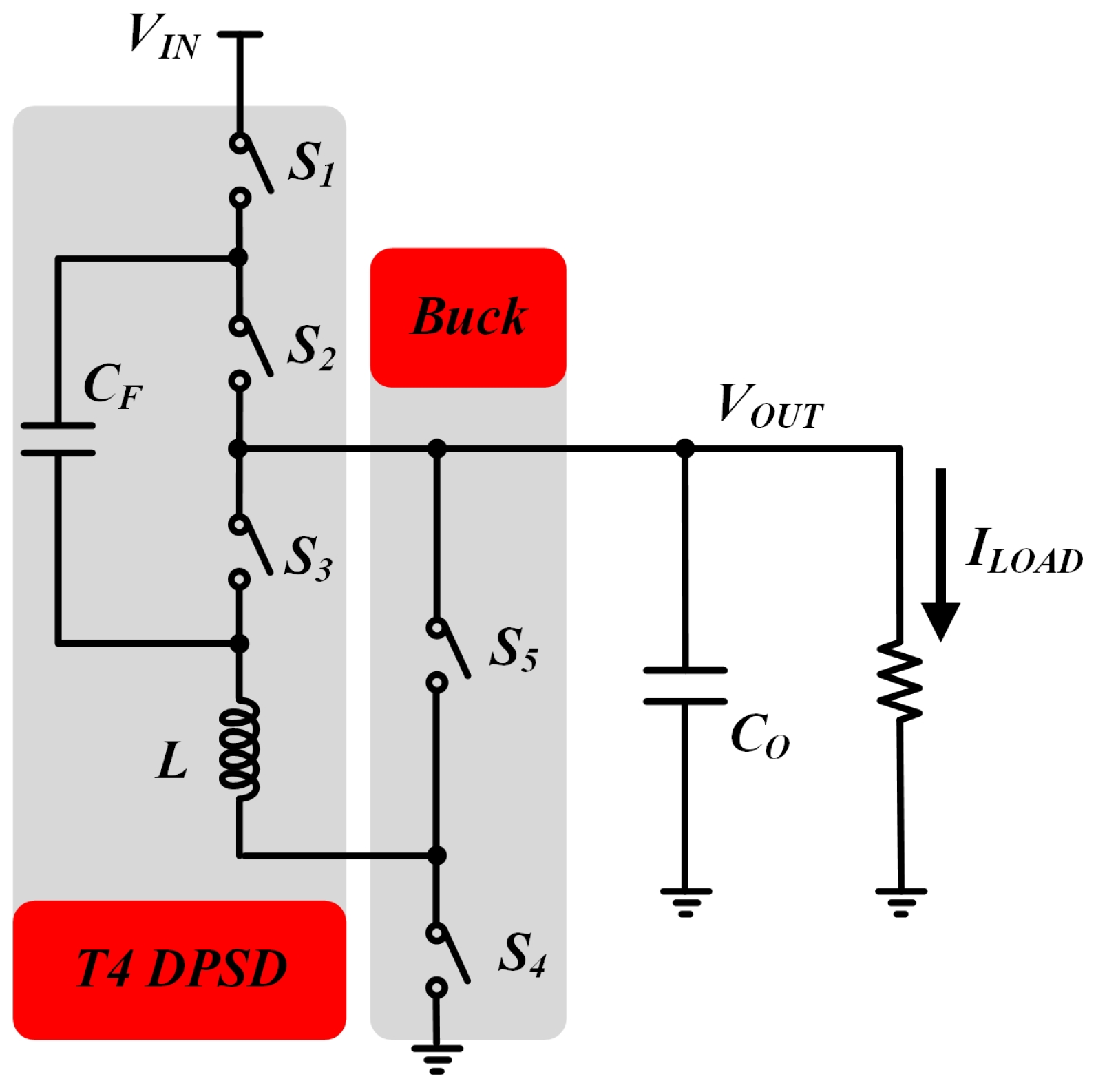
2. The Proposed Topology

2.1. Topology Transformation

The CBC, composed of power transistors S1 and S2, inductor L, and output capacitor CO as shown in Figure 1a, features a simple topological structure which is the most widely used. Its output range can cover from input voltage to GND. However, the maximum voltage stress on the switching transistor reaches the input voltage. Figure 1b presents the topological structure of the T4 DPSD. It is composed of power transistors S1–3, inductor L, and two capacitor CF and CO. Although the T4 DPSD reduces the switching voltage stress, its VCRs range is only 0 to 0.5.
By combining the advantages of both the CBC and T4 DPSD, the dual-path step-down converter with auxiliary switches achieves both wide-range voltage conversion ratios and reduced switching voltage stress. It is shown in Figure 2.

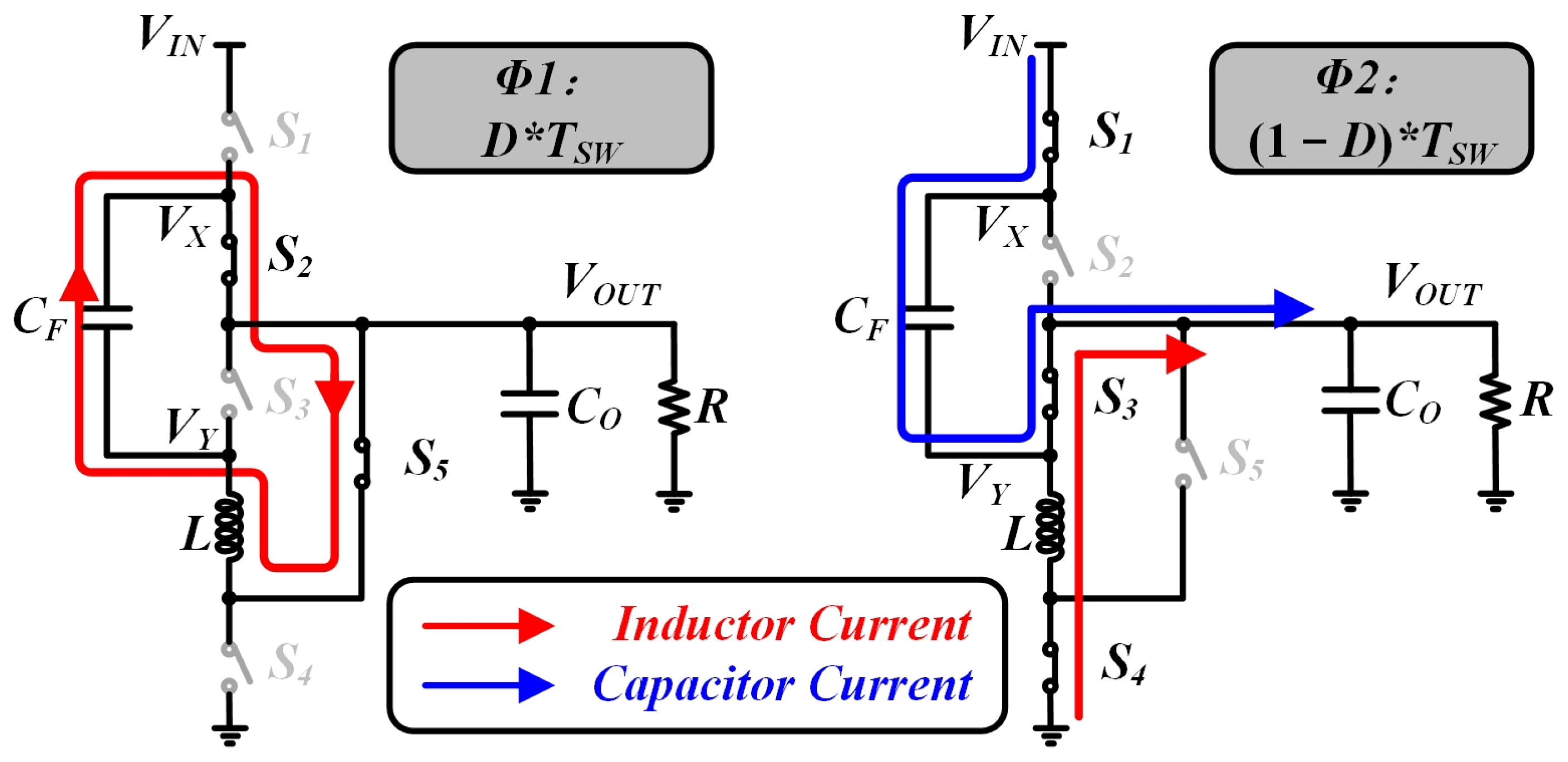
2.2. Operation of the Proposed Topology

Figure 3 illustrates the structural design of the proposed topology in detail, where D represents the duty cycle, and TSW denotes the unit period during normal operation of the topology. In Figure 3, the gray switches indicate that the switches are open, while the black switches represent that the switches are closed. It can be seen that the topology mainly consists of an inductor L, a flying capacitor CF, an output capacitor CO, and five switches S1–5.
Figure 3 provides a comprehensive illustration of the operating principle of the proposed topology. Specifically, during the Φ1 phase, S2 and S5 are switched on while S1, S3, and S4 are in the off state. As a result, a series connection is established between CF and L. At this point, CF charges the inductor. The situation changes when the operation reaches Φ2, where S1, S3, and S4 are on and S2 and S5 are off. At this point, CF is charged to the VINVOUT voltage level. At the same time, L discharges to the load.

2.3. Step-Down Conversion Ratios

Figure 3 demonstrates that the VY node voltage alternates between 2VOUTVIN and VOUT, driven by CF and the VX node voltage switching between VOUT and VIN. Based on this, the voltage conversion ratios of the proposed topology are calculated using the voltage-second balance method on inductor L:
( V I N V O U T ) D T S W V O U T ( 1 D ) T S W = 0
V O U T V I N = D
where D is the duty ratio, VIN/VOUT is the voltage conversion ratio, and TSW represents a switching period of the topology, which means one operating cycle of the topology. Like the CBC, the proposed converter achieves a full range of VCRs.

2.4. Switch Voltage Stress Reduction

In addition, during phase Φ1, switches S1 and S3 experience a voltage stress of VINVOUT, while S4 is subjected to VOUT. In phase Φ2, the voltage stress on S2 is VINVOUT, and S5 bears VOUT. Thanks to the presence of CF, the proposed topology achieves reduced voltage stresses across its switches compared to the CBC topology [7].

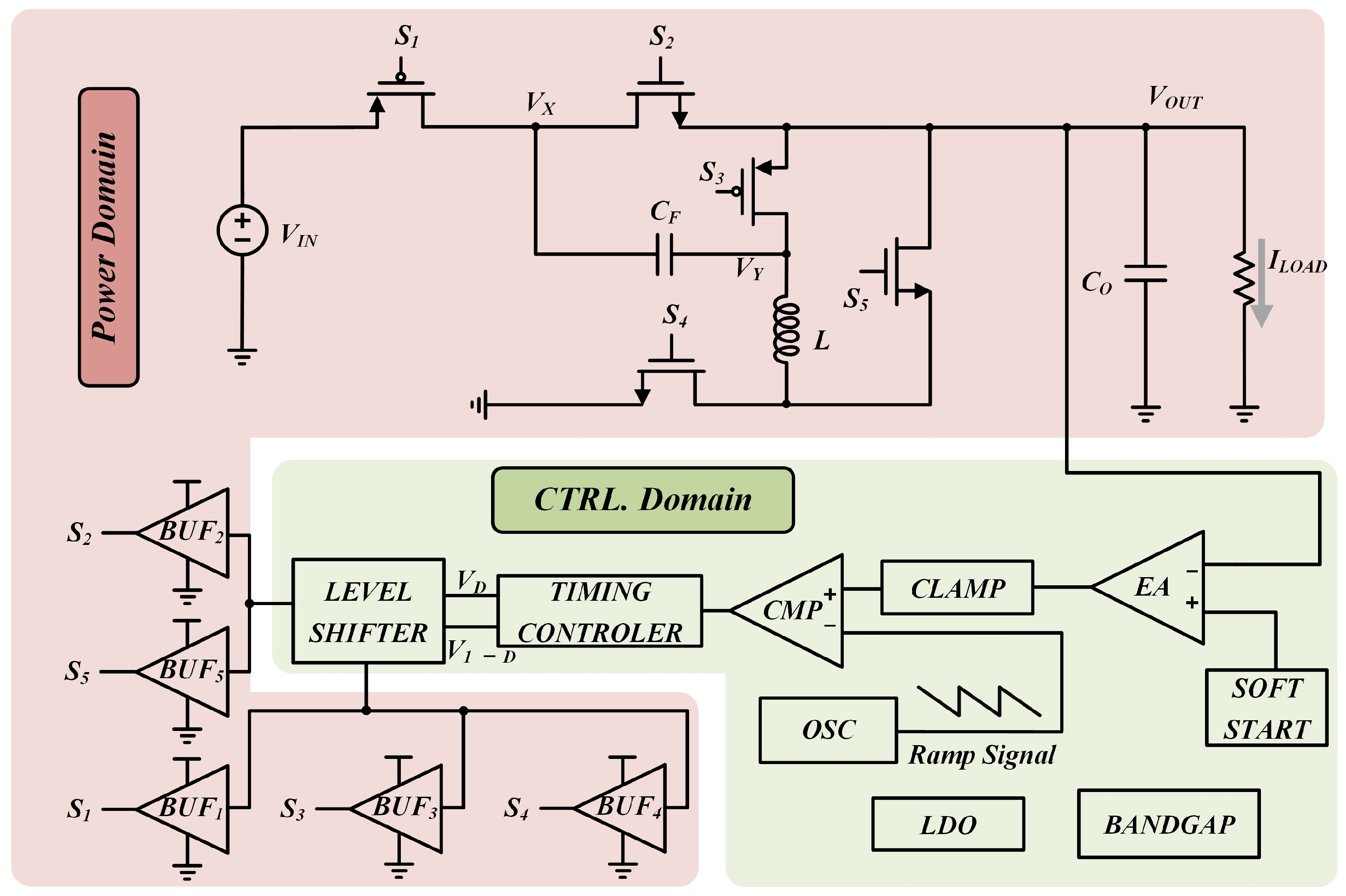
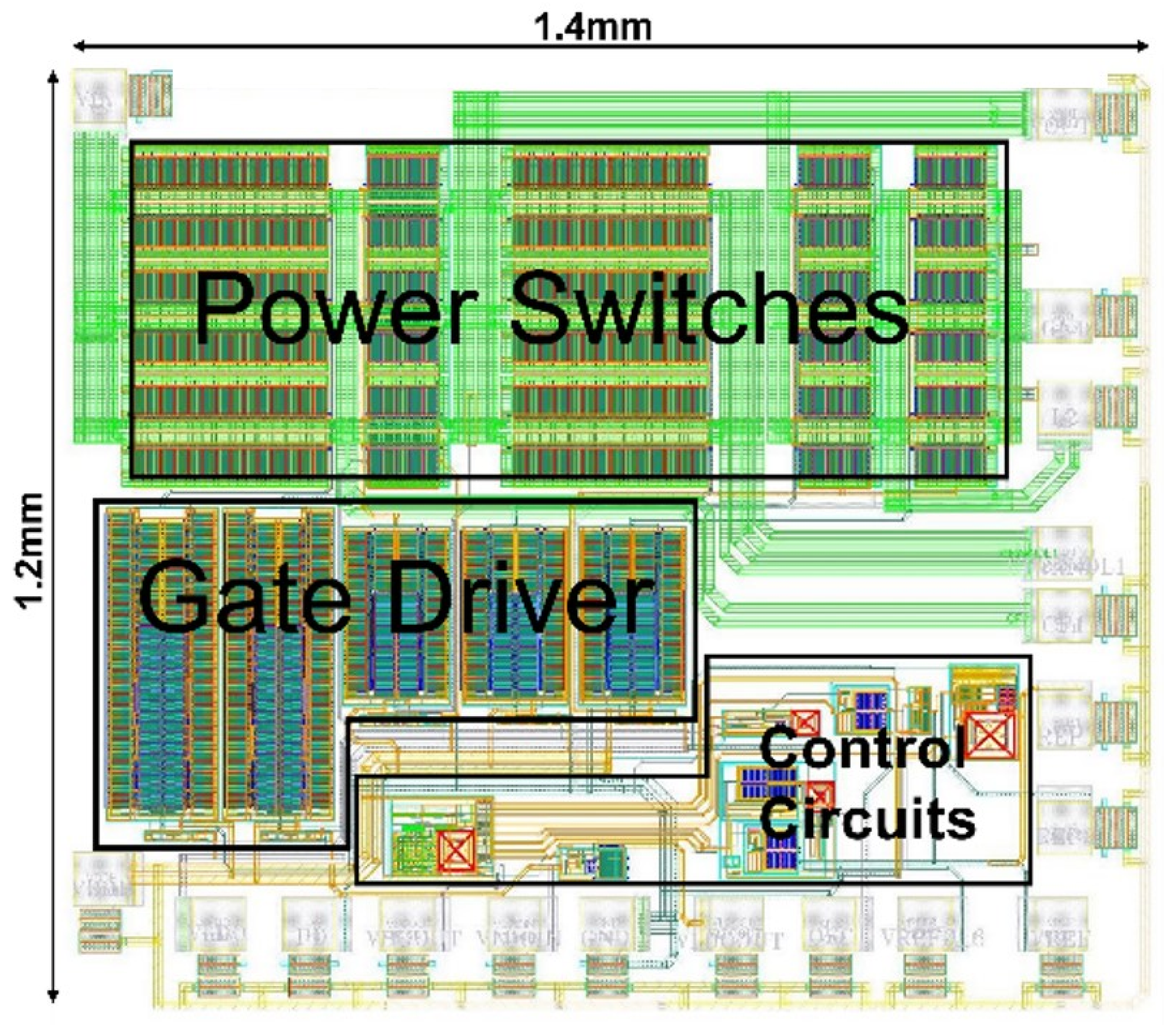
3. Circuit Implementation

This section provides a detailed depiction of the circuit implementation of the proposed converter. The overall structure of the converter is shown in Figure 4, which comprises switches S1 to S5 and the voltage-negative feedback controller.

3.1. Control Circuit

The proposed converters’ system can be roughly divided into the control domain and power domain, as shown in Figure 4.
The power domain includes power transistors and gate drivers, and the control domain includes an error amplifier (EA), soft start circuit, bandgap, oscillator (OSC), and timing controller.
In the power stage, the power switches S2 and S5 are turned ON, while S1, S3, and S4 are turned OFF during Φ1; during Φ2, S1, S3, and S4 are turned ON, while S2 and S5 are turned OFF. The voltage at VY can fall below the ground level during Φ1 due to the discharge of CF. During Φ2, VX reaches VIN because S1 closes. To minimize the number of off-chip components and simplify the circuit, S3 and S1 are implemented using PMOS transistors. The remaining switches are implemented with NMOS transistors.
In our design, the output voltage of the converter will be fed back into the negative voltage feedback loop. The error signal, resulting from the comparison between VOUT and Vrefss which is generated by the soft start circuit, undergoes comparison with the ramp signal from the oscillator. This generates a square wave signal that controls the duty cycle. To ensure proper operation of the power stage, level shifters are included in the design [7].
Therefore, to meet the performance requirements and ensure the functioning of the converter, Figure 5 presents the design flowchart of the proposed converter. The converter design begins with defining key specifications before proceeding to implement the control loop modules including bandgap reference, LDO regulator, error amplifier (EA), and oscillator (OSC). Subsequently, the power stage circuitry is constructed with optimized passive components and properly sized power switches, followed by critical loop compensation tuning. The design is finalized only after rigorous verification confirms all input/output characteristics and efficiency metrics meet target requirements, completing the comprehensive power converter development process.

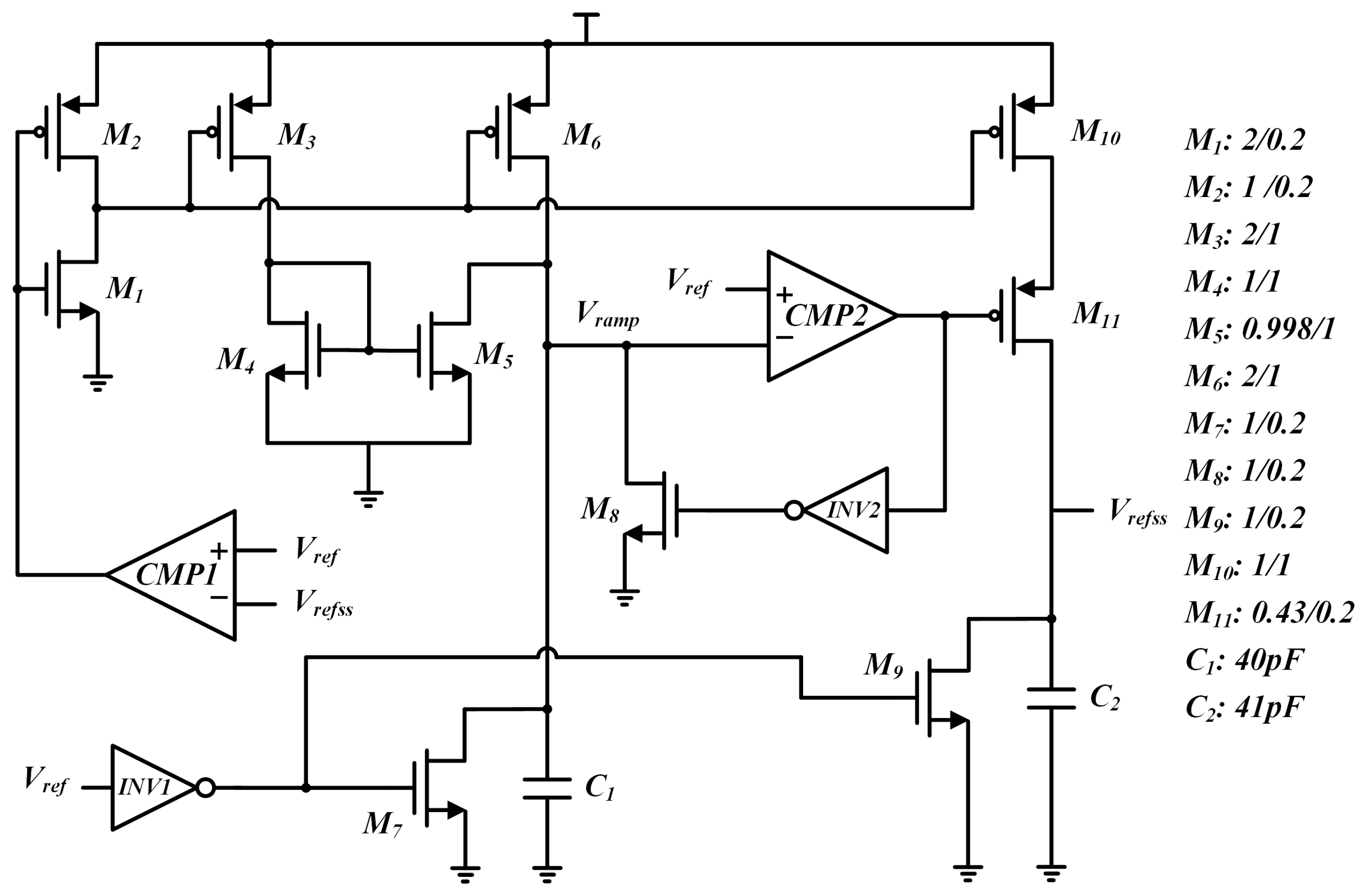
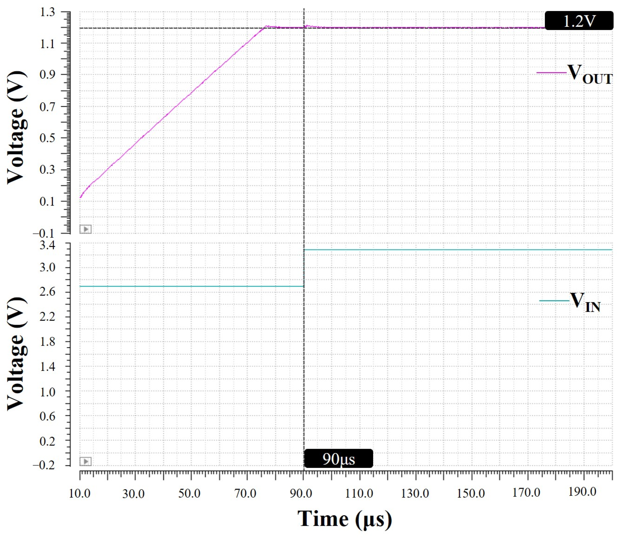
3.2. Soft-Start Circuit

During the start-up phase of a DC-DC converter, a significant voltage overshooting or large inrush current often occurs due to the substantial difference between the reference voltage and the output feedback voltage applied to the error amplifier [18]. For instance, a pulse-skipping soft-start circuit has been proposed to control the reference voltage of the error amplifier, effectively restraining the inrush current during start-up [19]. Additionally, an on-chip soft-start technique utilizing a staircase waveform signal generator to control the error amplifier’s output has demonstrated effectiveness in preventing inrush current and output voltage overshoot [20]. These approaches highlight the importance of managing the error amplifier’s input during start-up to ensure a smooth transition and stable operation of DC-DC converters. This article also describes a soft start circuit as depicted in Figure 6 [21,22].
During the start-up phase of a DC-DC converter, a significant voltage overshooting or large inrush current often occurs due to the substantial difference between the reference voltage and the output feedback voltage applied to the error amplifier. For instance, a pulse-skipping soft-start circuit has been proposed to control the reference voltage of the error amplifier, effectively restraining the inrush current during start-up [19]. Additionally, an on-chip soft-start technique utilizing a staircase waveform signal generator to control the error amplifier’s output has demonstrated effectiveness in preventing inrush current and output voltage overshoot [20]. These approaches highlight the importance of managing the error amplifier’s input during start-up to ensure a smooth transition and stable operation of DC-DC converters. This article also describes a soft start circuit as depicted in Figure 6 [21,22].
In Figure 6, the soft start circuit is formed by comparators CMP1CMP2, inverters INV1INV2, transistors M1M11, and capacitors C1C2.
At first, the output voltage (Vrefss) is set at zero because there is no charge on the C2. Vrefss is lower than the reference voltage (Vref), making M1 on so that the current mirrors M3–6, and M10 start to work.
By designing the dimensions of the transistor, the current flowing through M6 is slightly larger than that of M5. At this point, C1 is charged continuously. When the voltage of C1 is greater than Vref, M11 is on, the current flowing through M11 charges C2, and Vrefss slowly becomes larger. At the same time, the output of CMP2 is inverted and delayed by INV2, causing M8 on, grounding C1. Then, M8 is off keeping C1 charged again. Due to the periodic charging and discharging of C1, a ramp voltage (Vramp) is formed, causing Vrefss to slowly become larger until it is the same as Vref.

4. Simulation Result and Discussions

Here is the simulation result of the soft-start circuit in Figure 7.
This work, simulated in a 65 nm CMOS process, occupies an active area of 1.58 mm2, as shown in Figure 8. The layout consists of power switches, gate drivers, and control circuits.
For CO, it can be obtained from the capacitor charge formula:
Δ V O U T 1 C O 0 D T S W I L O A D d t = I L O A D D T S W C O
C O I L O A D V O U T T S W V I N Δ V O U T
where ∆VOUT represents the output ripple voltage, ILOAD represents the load current. After subsequent simulation verification and comprehensive consideration, the final choice for CO was 5 µF. To ensure the system always operates in continuous conduction mode (CCM), the peak-to-peak inductor current and the load current must satisfy the following relationship:
Δ I L = 1 L 0 D T S W V L d t = 1 L 0 D T S W V I N V O U T d t
Δ I L 2 I L O A D
L V O U T T S W V I N V O U T 2 V I N I L O A D
where ∆IL represents the peak-to-peak inductor ripple current. After simulation verification, the value of L is selected as 380 nH. As for the capacitor CF, currently, there is relatively little research on its value. We have set its value at 80 nF to facilitate the compensation of the system.
This experiment used a 380 nH external inductor, an 80 nF external capacitor for CF, and a 5 µF external capacitor for CO, shown in Table 1. The function of this converter is to convert 3.3 V into an output voltage of 1.2 V. Currently, much of the research on DC-DC converters is being conducted at a switching frequency of 10 MHz, which has become a hot topic in the field [23,24,25]. The higher frequencies increase switching losses but reduce the size of inductors and filters, enabling a more compact design and improving system response speed. While lower frequencies reduce switching losses, they increase component size and affect dynamic response. So, in this design, a working frequency of 10 MHz was selected for the DC-DC converter, based on a comprehensive consideration of switching losses, component size, system efficiency, fast response, and small volume.
For the size selection of power MOSFETs, it is essential to ensure a low on-resistance to maintain the load capability of the switching transistor circuit and avoid performance degradation due to current limitations. At the same time, the transistor’s switching performance and process adaptability must be ensured. A shorter transistor gate length improves switching speed and reduces switching losses, making it suitable for high-frequency applications [26,27]. Therefore, after comprehensive consideration, the sizes of the NMOS and PMOS power switching transistors were determined to be 35 × 600 µm/0.5 µm and 70 × 600 µm/0.5 µm.
Figure 9 shows the output voltage waveforms of the proposed converter with and without the soft-start circuit under the conditions of a 3.3 V input voltage and a 100 mA load current. It can be observed that without the soft-start circuit, a significant voltage deviation occurs between the output voltage and the expected value during the initial start-up phase. This causes the error amplifier to exit its linear operating region, while the comparator generates a PWM signal with a large duty cycle, forcing the output voltage to rapidly approach the reference voltage. However, due to the demagnetization delay of the inductor current and the low loop gain and bandwidth during start-up period, the converter’s feedback loop exhibits a certain lag. During the inductor demagnetization phase, the released energy superimposes onto the output voltage, resulting in voltage overshoot, which may damage the circuit. With the soft-start circuit, the output voltage increases gradually and stabilizes near the reference voltage, significantly mitigating the overshoot issue.
Figure 10a shows the simulation results of the time control signal when VIN = 3.3 V and ILOAD = 100 mA. Figure 10b represents the simulation results of the relationship between the duty cycle D of the converter and ILOAD under the condition VIN = 3.3 V. According to Figure 10b, when ILOAD is small, the actual value of the D is approximately the same as the theoretically calculated value of VOUT/VIN (36.4%). However, as ILOAD increases, the D of the converter will gradually be larger than its theoretically calculated value. As the load current increases, the inductor requires more energy to maintain the output. Therefore, in order to ensure that the output remains constant, the time for CF to charge the inductor needs to be extended, that is, D needs to increase. The voltage across CF will gradually decrease during the inductor charging phase. This situation is not obvious when the load is light, but when the load is heavy, this phenomenon will be magnified, thus further increasing the charging gain time of the inductor current. Therefore, D will increase as ILOAD increases. According to Figure 10b, when the load current is less than 0.1 A, the duty cycle can be approximately regarded as being unaffected by the load current.
To detect the robustness of the converter, the waveform of the converter’s output voltage when the input voltage undergoes an instantaneous change is shown in Figure 11. At Time = 90 µs, VIN changes from 2.7 V to 3.3 V. At this time, the VOUT will experience a brief spike fluctuation, with the peak voltage reaching 1.215 V. After this short-term fluctuation, the output voltage continues to be stably output.
Figure 12 presents the simulated efficiency versus load current characteristics of the converter under different input voltages. The converter achieves a peak efficiency of 90.6% at VIN = 2.7 V and ILOAD = 70 mA. Under higher step-down ratios with VIN = 3 V and VIN = 3.3 V, the peak efficiency remains above 88%.
Table 2 presents the summary and comparison with the state-of-the-art. The proposed converter uses five CMOS power switches but still achieves a conversion efficiency of over 90%. As shown in Table 2, the proposed converter maintains comparable peak efficiency while achieving lower voltage stress on power switches compared to reference [8]. Furthermore, the adopted topology demonstrates wider step-down conversion ratios than those in references [12,13,14], enabling broader application scenarios.

5. Conclusions

This article has presented a dual-path step-down converter with auxiliary switches and soft-start circuit. The proposed converter, designed for low-power systems, uses a 65 nm CMOS process with a layout area of only 1.58 mm2. The converter can realize lithium-ion battery voltage to 1.2 V voltage conversion and output more than 600 mA current load capacity, reaching a peak efficiency of 90%. The proposed topology can not only feature a full range of buck conversion ratios but also reduce switching voltage stress in the power stage circuit. Due to the soft-start circuit design, large inrush is suppressed. These design points improve the reliability and lifetime of the DC-DC converter, making it a new power-supply choice for low-power systems.

Author Contributions

Conceptualization, X.W. and Z.L. (Zishuo Li); methodology, Z.L. (Zhen Lin); software, F.M.; validation, Z.L. (Zishuo Li); formal analysis, X.W.; investigation, Z.L. (Zishuo Li) and Z.L. (Zhen Lin); resources, X.W. and F.M.; data curation, X.W.; writing—original draft preparation, Z.L. (Zishuo Li); writing—review and editing, Z.L. (Zishuo Li) and F.M.; visualization, X.W.; supervision, F.M.; project administration, F.M. All authors have read and agreed to the published version of the manuscript.

Funding

This research was funded by the National Natural Science Foundation of China: Project 62271347 and U21A20459.

Data Availability Statement

All original contributions discussed in this study are contained within the article. For additional information, please contact the corresponding authors.

Conflicts of Interest

Author Xin Wang from China Electronics Technology Group Corporation. The authors declare no conflict of interest.

References

  1. Ahsanuzzaman, S.M.; Prodić, A.; Johns, D.A. An Integrated High-Density Power Management Solution for Portable Applications Based on a Multioutput Switched-Capacitor Circuit. IEEE Trans. Power Electron. 2016, 31, 4305–4323. [Google Scholar] [CrossRef]
  2. Renz, P.; Kaufmann, M.; Lueders, M.; Wicht, B. Switch Stacking in Power Management ICs. IEEE J. Emerg. Sel. Top. Power Electron. 2021, 9, 3735–3743. [Google Scholar] [CrossRef]
  3. Shi, C.; Walker, B.C.; Zeisel, E.; Hu, B.; McAllister, G.H. A Highly Integrated Power Management IC for Advanced Mobile Applications. IEEE J. Solid-State Circuits 2007, 42, 1723–1731. [Google Scholar]
  4. Meng, F.; Disney, D.; Liu, B.; Volkan, Y.B.; Zhou, A.; Liang, Z.; Yi, X.; Selvaraj, S.L.; Peng, L.; Ma, K.; et al. Heterogeneous Integration of GaN and BCD Technologies and Its Applications to High Conversion-Ratio DC-DC Boost Converter IC. IEEE Trans. Power Electron. 2019, 34, 1993–1996. [Google Scholar] [CrossRef]
  5. Disney, D.; Shen, Z.J. Review of Silicon Power Semiconductor Technologies for Power Supply on Chip and Power Supply in Package Applications. IEEE Trans. Power Electron. 2013, 28, 4168–4181. [Google Scholar] [CrossRef]
  6. Wu, P.Y.; Tsui, S.Y.S.; Mok, P.K.T. Area- and Power-Efficient Monolithic Buck Converters with Pseudo-Type III Compensation. IEEE J. Solid-State Circuits 2010, 45, 1446–1455. [Google Scholar] [CrossRef]
  7. Li, Z.; Lin, Z.; Meng, F. A Single Active Phase Hybrid Buck Converter with Reduced Voltage Stress and Wide Voltage Conversion Ratios for Integrated Terahertz Systems. In Proceedings of the 5th China and International Young Scientist Terahertz Conference, Chengdu, China, 22–24 March 2024; Chang, C., Zhang, Y., Zhao, Z., Zhu, Y., Eds.; Springer Science and Business Media, LLC: Singapore, 2024; Volume 2, pp. 200–204. [Google Scholar]
  8. Du, M.; Lee, H.; Liu, J. A 5MHz 91% Peak-Power-Efficiency Buck Regulator with Auto-Selectable Peak and Valley-Current Control. IEEE J. Solid-State Circuits 2011, 46, 1928–1939. [Google Scholar] [CrossRef]
  9. Son, H.S.; Kim, J.K.; Lee, J.B.; Moon, S.S.; Park, J.H.; Lee, S.H. A New Buck–Boost Converter with Low-Voltage Stress and Reduced Conducting Components. IEEE Trans. Ind. Electron. 2017, 64, 7030–7038. [Google Scholar] [CrossRef]
  10. Pan, C.T.; Chuang, C.F.; Chu, C.C. A Novel Transformerless Interleaved High Step-Down Conversion Ratio DC-DC Converter with Low Switch Voltage Stress. IEEE Trans. Ind. Electron. 2014, 61, 5290–5299. [Google Scholar] [CrossRef]
  11. Kozak, J.P.; Song, Q.; Zhang, R.; Ma, Y.; Liu, J.; Li, Q.; Saito, W.; Zhang, Y. Degradation and Recovery of GaN HEMTs in Overvoltage Hard Switching Near Breakdown Voltage. IEEE Trans. Power Electron. 2023, 38, 435–446. [Google Scholar] [CrossRef]
  12. Hata, K.; Yamauchi, Y.; Sai, T.; Sakurai, T.; Takamiya, M. 48V-to-12V Dual-Path Hybrid DC-DC Converter. In Proceedings of the 2020 IEEE Applied Power Electronics Conference and Exposition (APEC), New Orleans, LA, USA, 15–19 March 2020; pp. 2279–2284. [Google Scholar]
  13. Zhen, S.; Yang, R.; Wu, D.; Cheng, Y.; Luo, P.; Zhang, B. Design of Hybrid Dual-Path DC-DC Converter with Wide Input Voltage Efficiency Improvement. In Proceedings of the 2021 IEEE International Symposium on Circuits and Systems (ISCAS), Daegu, Republic of Korea, 22–28 May 2021; pp. 1–5. [Google Scholar]
  14. Cai, G.; Lu, Y.; Martins, R.P. An SC-Parallel-Inductor Hybrid Buck Converter with Reduced Inductor Voltage and Current. IEEE J. Solid-State Circuits 2023, 58, 1758–1768. [Google Scholar] [CrossRef]
  15. Zhang, D.; Sha, D.; Gao, C.; Liu, X.; Long, H.; Tang, G.; Zhao, Y.; Gao, Y. A Closed-Loop Soft Start up Strategy to Suppress Inrush Current for Full-Bridge Modular Multilevel Converters. IEEE Trans. Power Electron. 2024, 39, 14787–14799. [Google Scholar] [CrossRef]
  16. Al-Shyoukh, M.; Lee, H. A Compact Fully-Integrated Extremum-Selector-Based Soft-Start Circuit for Voltage Regulators in Bulk CMOS Technologies. IEEE Trans. Circuits Syst. II Express Briefs 2010, 57, 818–822. [Google Scholar] [CrossRef]
  17. Goyal, S.; Wadhwa, S.K.; Tripathi, D. An RC charging based Soft-Start circuit for Voltage Regulators. In Proceedings of the 2022 IEEE Region 10 Symposium (TENSYMP), Mumbai, India, 1–3 July 2022; pp. 1–4. [Google Scholar]
  18. Al-Shyoukh, M.; Lee, H. A Compact Ramp-Based Soft-Start Circuit for Voltage Regulators. IEEE Trans. Circuits Syst. II Express Briefs 2009, 56, 535–539. [Google Scholar] [CrossRef]
  19. Liu, P.J.; Hsu, Y.C.; Chang, Y.H. A Current-Mode Buck Converter with a Pulse-skipping Soft-start Circuit. In Proceedings of the 2013 IEEE 10th International Conference on Power Electronics and Drive Systems (PEDS), Kitakyushu, Japan, 22–25 April 2013; pp. 262–265. [Google Scholar]
  20. Jing, X.; Mok, P.K.T. Soft-Start Circuit with Duty Ratio Controlled Voltage Clamping and Adaptive Sizing Technique for Integrated DC-DC Converters. In Proceedings of the 2010 IEEE International Conference of Electron Devices and Solid-State Circuits (EDSSC), Hong Kong, China, 15–17 December 2010; pp. 1–4. [Google Scholar]
  21. Liu, P.J.; Hsu, C.Y.; Chang, Y.H. Techniques of Dual-Path Error Amplifier and Capacitor Multiplier for On-Chip Compensation and Soft-Start Function. IEEE Trans. Power Electron. 2015, 30, 1403–1410. [Google Scholar] [CrossRef]
  22. Tiwari, A.A.; Mishra, D.K. A DC-DC Boost Converter with Soft Start Function and DPEA Technique Using 180nm Technology. In Proceedings of the 2017 International Conference on Information, Communication, Instrumentation and Control (ICICIC), Indore, India, 17–19 August 2017; pp. 1–6. [Google Scholar]
  23. Magni, G.; Melillo, P.; Bertolini, A.; Leoncini, M.; Ghioni, M. A 10-MHz Three-Level Buck Converter with Dual-Loop Time-Based Control and Flying Capacitor Voltage-Balance for Fast DVS. In Proceedings of the 2024 19th Conference on Ph.D Research in Microelectronics and Electronics (PRIME), Larnaca, Cyprus, 9–12 June 2024; pp. 1–4. [Google Scholar]
  24. Li, W.S.; Zhou, D.C.; Yan, H.; Zhang, J.F.; Ma, H.H.; Chen, C.; Huang, J.B.; Liu, X.M.; Li, W.P.; Wu, M.; et al. Dynamic Rdson and Vth Free 15 V E-mode GaN HEMT Delivering Low sFOM of 13.1 mΩ•nC and over 90% Efficiency at 10 MHz for Buck Converter. In Proceedings of the 2022 IEEE 34th International Symposium on Power Semiconductor Devices and ICs (ISPSD), Vancouver, BC, Canada, 22–25 May 2022; pp. 161–164. [Google Scholar]
  25. Agarwal, S.; Maity, A. A 10-MHz Current-Mode Fixed-Frequency Hysteretic Controlled DC-DC Converter with Fast Transient Response. In Proceedings of the 2019 IEEE 62nd International Midwest Symposium on Circuits and Systems (MWSCAS), Dallas, TX, USA, 4–7 August 2019; pp. 945–948. [Google Scholar]
  26. Crupi, G.; Schreurs, D.M.M.-P.; Caddemi, A. Effects of Gate-Length Scaling on Microwave MOSFET Performance. Electronics 2017, 6, 62. [Google Scholar] [CrossRef]
  27. Zhu, Q.; Zhang, T.; Wang, J.; Cheng, Y. Design and Layout realization of Power MOSFET in Switching Power Supply. In Proceedings of the 2023 5th International Conference on Electronic Engineering and Informatics (EEI), Wuhan, China, 30 June–2 July 2023; pp. 99–103. [Google Scholar]
Figure 1. (a) Schematic of CBC. (b) Schematic of T4 DPSD.
Jlpea 15 00029 g001
Figure 2. Schematic drawing and transformation process of the proposed topology.
Jlpea 15 00029 g002
Figure 3. Structure and operation of the proposed topology.
Jlpea 15 00029 g003
Figure 4. Total block diagram of the proposed converter.
Jlpea 15 00029 g004
Figure 5. Design flowchart.
Jlpea 15 00029 g005
Figure 6. Schematic diagram of soft-start circuit.
Jlpea 15 00029 g006
Figure 7. Simulation result of soft-start circuit.
Jlpea 15 00029 g007
Figure 8. Layout of proposed converter.
Jlpea 15 00029 g008
Figure 9. Output voltage waveform of the converter.
Jlpea 15 00029 g009
Figure 10. (a) Timing-control signal. (b) The duty cycle under different load current conditions.
Jlpea 15 00029 g010
Figure 11. Waveform of the output voltage when the input voltage undergoes a transient change.
Jlpea 15 00029 g011
Figure 12. Converter efficiency under variable load conditions.
Jlpea 15 00029 g012
Table 1. Main design parameters of the proposed converter.
ParameterValue
Output capacitor, Co5 µF
Inductor, L380 nH
Flying capacitor, CF80 nF
NMOS power switch35 × 600 µm/0.5 um
PMOS power switch70 × 600 µm/0.5 um
Output voltage, VOUT1.2 V
Expected load current200 mA
Table 2. Performance summary and comparison.
This Work *[8]
JSSC 2011 #
[12]
APEC 2020 #
[13]
ISCAS 2021 *
[14]
JSSC 2022 #
Process65 nm CMOS0.35 µm CMOSPCB0.18 µm BCD65 nm CMOS
TopologyDPSD with
Auxiliary Switches
BuckDPSDDPSDCPL-Buck
Frequency10 MHz5 MHz100 kHz1 MHz2 MHz
Peak
Efficiency
90.6%91%97.1%95.6%92.9%
Input Voltage [V]2.7–42.7–4.2482.7–53.0–4.2
Output
Voltage [V]
1.2N/A121.20.6–1.0
Number of
Power Switches
52336
Main Switch Voltage Stress [V]VINVOUT, VOUTVINVINVOUTVINVOUTVINVOUT, VOUT
Topology VCRsDDD/(1 + D)D/(1 + D)D/(1 + 2D) or D/(1 + D)
* Based on simulation results; # Based on measurement results.
Disclaimer/Publisher’s Note: The statements, opinions and data contained in all publications are solely those of the individual author(s) and contributor(s) and not of MDPI and/or the editor(s). MDPI and/or the editor(s) disclaim responsibility for any injury to people or property resulting from any ideas, methods, instructions or products referred to in the content.

