Article

A CMOS Switched Capacitor Filter Based Potentiometric Readout Circuit for pH Sensing System

by
Shanthala Lakshminarayana
1,
Revathy Perumalsamy
2,
Chenyun Pan
1,
Sungyong Jung
3,
Hoon-Ju Chung
4,* and
Hyusim Park
5,*
1
Department of Electrical Engineering, University of Texas at Arlington, Arlington, TX 76019, USA
2
Sr. Staff ATE Engineer, Movandi, CA 92618, USA
3
Department of Electrical & Computer Engineering, South Dakota State University, Brookings, SD 57007, USA
4
School of Electronic Engineering, Kumoh National Institute of Technology, Gumi 39177, Republic of Korea
5
Department of Electrical Engineering, University of North Texas, Dallas, TX 75241, USA
*
Authors to whom correspondence should be addressed.
J. Low Power Electron. Appl. 2025, 15(1), 3; https://doi.org/10.3390/jlpea15010003
Submission received: 9 December 2024 / Revised: 17 January 2025 / Accepted: 18 January 2025 / Published: 19 January 2025

Abstract

:
This work presents a potentiometric readout circuit for a pH-sensing system in an oral healthcare device. For in vivo applications, noise, area, and power consumption of the readout electronics play critical roles. While CMOS amplifiers are commonly used in readout circuits for these applications, their applicability is limited due to non-deterministic noises such as flicker and thermal noise. To address these challenges, the Correlated Double Sampler (CDS) topology is widely employed as a sampled-data circuit for potentiometric readout, effectively eliminating DC offset and drift, thereby reducing overall noise. Therefore, this work introduces a novel potentiometric readout circuit realized with CDS and a switched-capacitor-based low-pass filter (SC-LPF) to enhance the noise characteristic of overall circuit. The proposed readout circuit is implemented in an integrated circuit using 0.18 µm CMOS process, which occupies an area of 990 µm × 216 µm. To validate the circuit performances, simulations were conducted with a 5 pF load and a 1 MHz input clock. The readout circuit operates with a supply voltage range ±1.65 V and linearly reproduces the pH sensor output of ±1.5 V. Noise measured with a 1 MHz sampling clock shows 0.683 µ V r m s , with a power consumption of 124.1 µW.

1. Introduction

The accurate measurement of pH, which quantifies the acidity or alkalinity of a substance, is a fundamental analytical technique with widespread applications across various fields, including biomedicine, chemistry, agriculture, and environmental monitoring. In biomedical applications, pH measurement is critical for assessing physiological conditions such as metabolic processes, body fluid composition, and the early detection of diseases [1,2,3,4,5,6,7,8,9,10,11,12,13]. For example, the regulation of oral pH plays a pivotal role in maintaining oral health, as fluctuations in pH can influence the onset of dental decay, gum diseases, and other oral infections. Elevated acid levels in the mouth, often caused by sugar consumption, lead to a pH drop below 5.5, initiating demineralization of the enamel and contributing to tooth erosion and cavity formation. Over time, persistent oral pH imbalances can exacerbate conditions such as periodontitis, xerostomia, and even systemic diseases like cardiovascular issues induced by oral inflammation [9,10].
The conventional method for pH measurement in electrochemical sensing is potentiometry, which operates by detecting the potential difference between a reference electrode and an indicator electrode. Among the most widely employed potentiometric sensors, glass electrodes offer a high degree of accuracy and linearity. However, these electrodes are bulky and unsuitable for in vivo applications, particularly in clinical or wearable devices, due to their large size and fragility [11,12,13]. An alternative to glass electrodes is the Ion Selective Field Effect Transistor (ISFET), which has gained attention due to its compact size, high sensitivity, and suitability for miniaturization. The ISFET sensor consists of a Metal Oxide Semiconductor Field Effect Transistor (MOSFET) configuration, where the gate is modified with an ion-selective membrane that responds to pH changes in the solution [14,15,16,17]. Changes in pH induce variations in the gate potential, which, in turn, modulate the current between the source and drain terminals, enabling the conversion of pH into an electrical signal. Despite significant advancements in ISFET technology, the integration of ISFETs with analog front-end circuits presents several challenges, particularly for in vivo applications. The main difficulties lie in optimizing the noise performance, minimizing power consumption, and achieving compactness in the design. In vivo pH-sensing applications, such as continuous oral health monitoring, require the balancing of these factors while ensuring that the circuit remains small and power efficient. Traditional analog front-end circuits for potentiometric sensors often suffer from high power consumption and large noise levels, particularly due to the intrinsic “1/f noise” (flicker noise) associated with CMOS transistors at low frequencies [18,19,20,21,22,23,24,25,26,27,28,29]. Given that pH sensors typically operate in the low-frequency range, managing noise becomes a critical aspect of ensuring accurate and reliable measurements.
This paper addresses the challenges associated with ISFET-based pH sensing by proposing a novel analog front-end circuit design that minimizes noise, reduces power consumption, and ensures miniaturization. The circuit incorporates advanced compensation techniques, including a switched-capacitor low-pass filter (SC-LPF) and a Correlated Double Sampler (CDS), to improve noise performance and mitigate issues related to drift and offset. These innovations allow for accurate, low-noise pH measurements, making the circuit suitable for real-time, in vivo oral healthcare applications.
The rest of this paper is organized into the following sections. Section 2 explains the proposed design of CDS with the SC-LPF built in 0.18 µm CMOS process for the pH-sensing system. Section 3 describes the post layout simulated results of circuit compared with other existing architectures. Section 4 concludes the proposed architecture presented in this work.

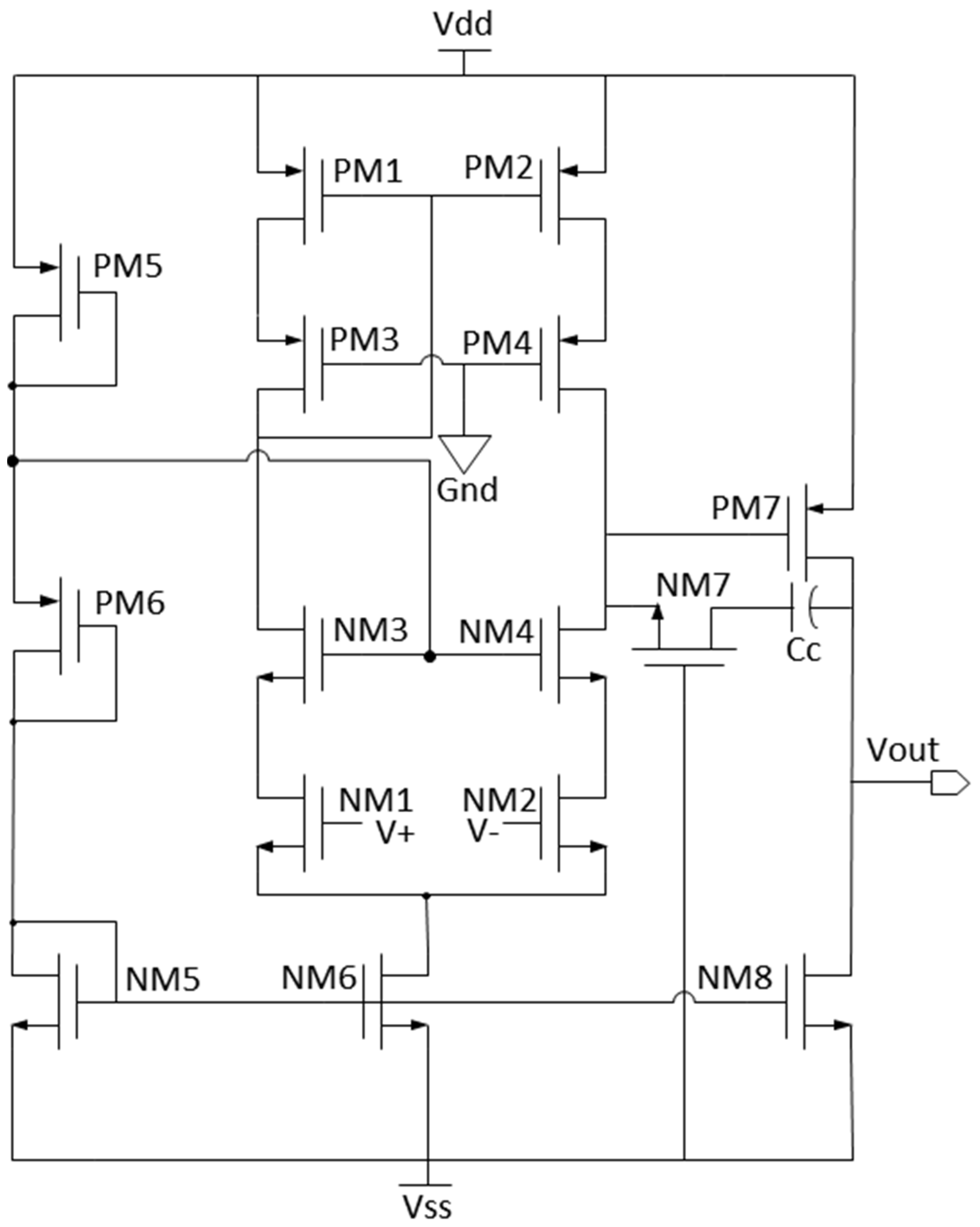
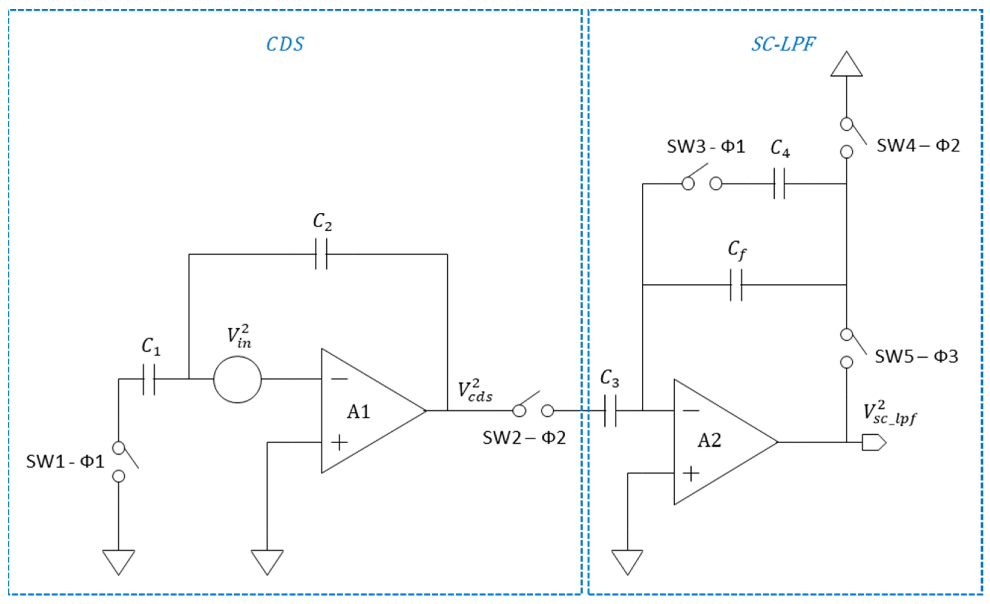
2. Design of Readout Circuit

The aim of this work is to build a potentiometric readout circuit with low noise and low power consumption that can convert the output of an ideal ISFET pH sensor, which has a sensitivity of 59.16 mV/pH according to the Nernst equation with an output voltage range of ±414 mV [30,31,32], or an ISFET pH sensor beyond the Nernst equation, with a sensitivity up to 200 mV/pH and a maximum output voltage range of ±1.5 V [33,34,35]. The Magnachip 0.18 µm CMOS process is chosen to design the readout circuit because of its attractive features such as an accurate and stable results with temperature changes, easy offset correction, rail-to-rail output, and linear voltage changes. In this work, the design of the potentiometric readout for pH sensing is accomplished in following two stages to conduct a comprehensive analysis: (a) CDS and (b) CDS followed by SC-LPF. Table 1 presents a list of abbreviations and symbols for the reader’s convenience.

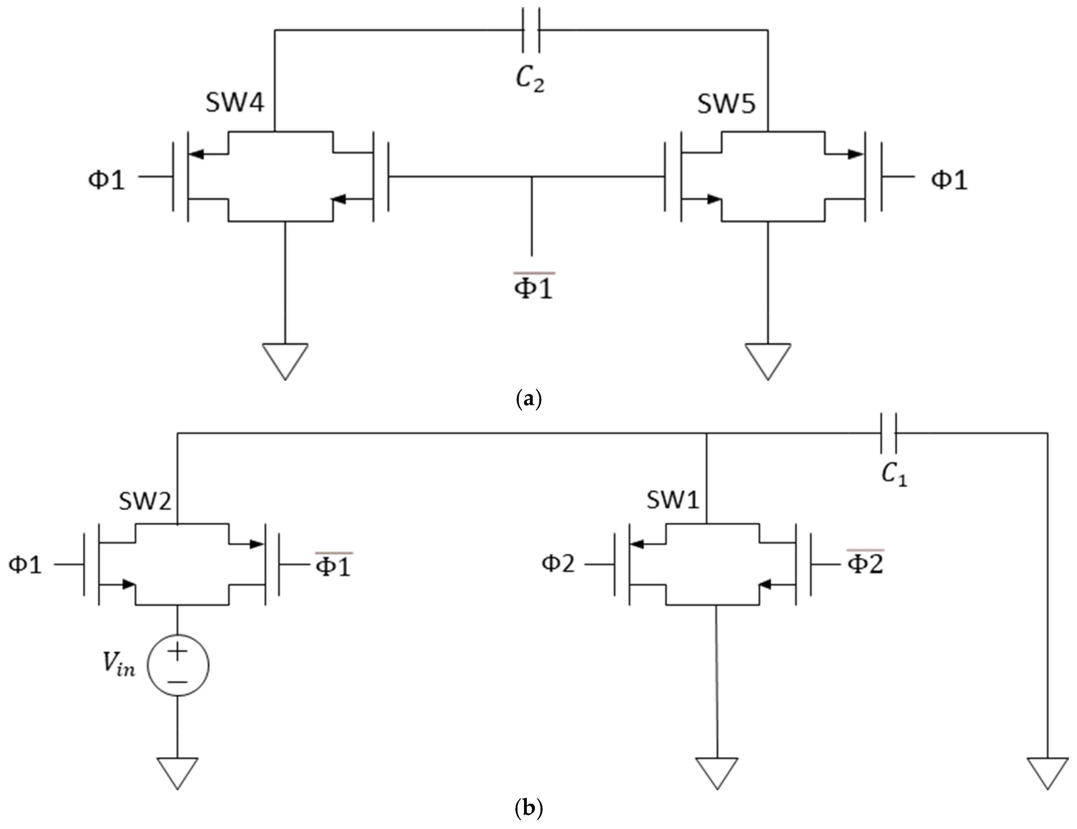
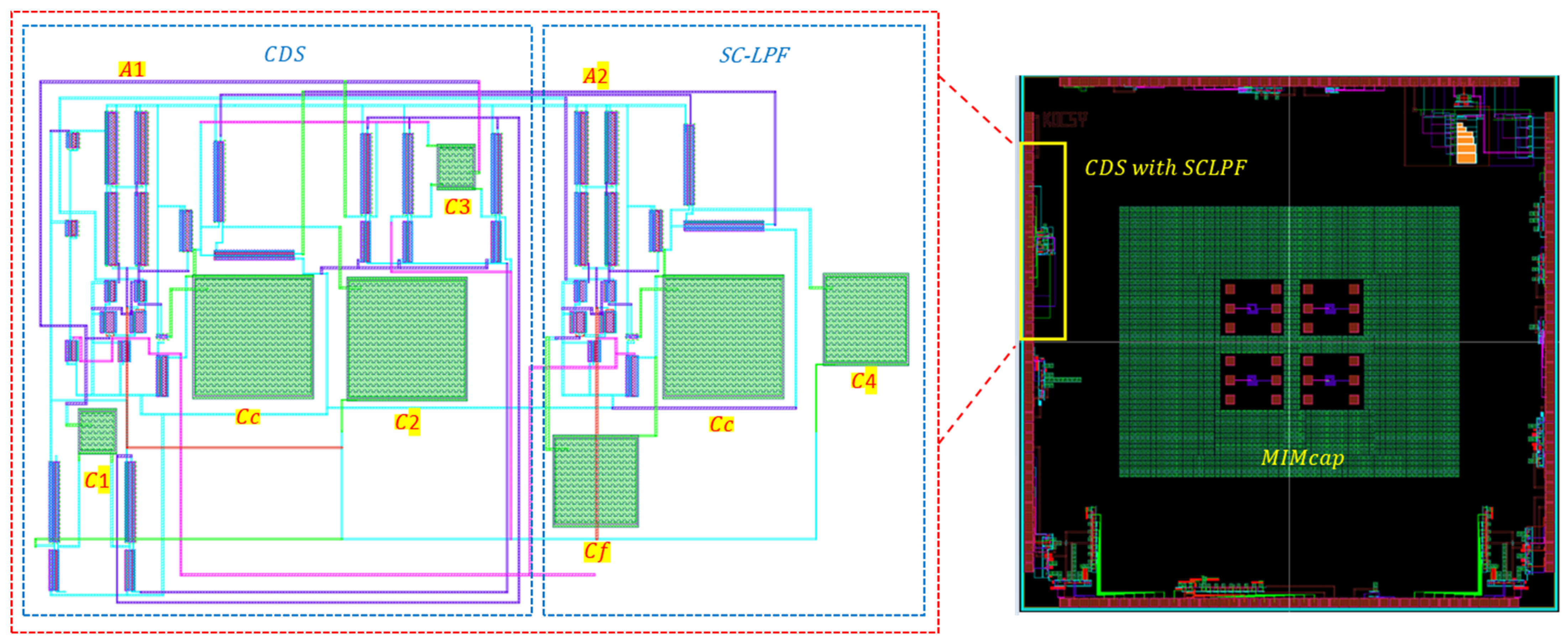
2.1. CMOS Correlated Double Sampler

A pH-sensing system using an ISFET is typically a 3-electrode system with source, drain, and gate electrodes of ISFET, as depicted in Figure 1. The reference electrode is the gate of ISFET, which is separated from the silicon dioxide, needed to establish a stable potential. Reference electrodes help to eliminate potential drifts caused by the solution itself and allow for accurate pH sensing. When the ISFET is exposed to a solution with a specific pH, the surface potential of the sensitive gate changes, altering the threshold voltage V t h of the ISFET, thereby changing the drain current flowing through the transistor. The voltage difference between the ISFET drain and the reference electrode is amplified by an operational amplifier (OPAMP), effectively eliminating common-mode noise and providing a high-sensitivity output signal directly proportional to the pH change.
The dominant noise sources in modern CMOS architectures are thermal noise and flicker noise. In CMOS transistors, thermal noise is created by the drain current fluctuations caused by a random motion of charge carriers, while flicker noise arises from the trapping of charges as they move from source to drain of the transistor. The voltage spectra of thermal and flicker in CMOS transistors are given by Equation (1) and (2), respectively [36,37,38,39].
V t h 2 Δ f = 4 K T γ g m
V f 2 Δ f = K f C o x W L f  
where K is the Boltzmann constant 1.38 × 10⁻²³ J/K, γ is 2 / 3 , T is the absolute temperature in degrees Kelvin, g m is the transconductance of the transistor, K f is the flicker noise coefficient, which depends on the technology, C o x is the gate oxide capacitance per unit area, W and L are the transistor gate width and length, respectively, f is the operating frequency, and Δ f is the small bandwidth at the frequency of f. The input voltage noise spectral density increases significantly as frequency decreases below the corner frequency, which may range anywhere between a few Hz and several hundred Hz. Generally, potentiometric sensors operate at low frequencies where flicker noise is dominant. Thus, to reduce the noise of the potentiometric readout circuit, the CDS circuit is widely embarked in the process of digitizing the potentiometric sensor output [36,37,38].
The CDS circuit architecture consists of an input resistor ( R i n ) and a feedback resistor ( R f ) designed with resistor emulators instead of passive resistors, as illustrated in Figure 1. The resistor emulators are built using a switched capacitor circuit where the switches are realized with transmission gates. Since the circuit operates at low frequency and considering that integrable capacitances are typically on the order of a few pF, the resulting resistances would range from hundreds of KΩ to MΩ, making the implementation with switched capacitor circuits essential. The operation of the switched capacitor in the CDS circuit includes two steps: sampling and integration, i.e., the signal generated by the sensor ( V i n ) can be sampled in a capacitor and then amplified with the help of an OPAMP which is ‘A1’. Utilizing two non-overlapping clocks (Φ1 and Φ2), the signal is sampled and stored in the capacitor. When Φ2 is high, the switch ‘SW1’ transfers the charge stored in the C 1 to C 2 and ‘A1’ allows the charge to be transferred to the output without loading. Meanwhile, when Φ1 is high, the C 2 is discharged and prepared for the next sample transfer, while the C 1 charges.
Figure 2 illustrates the implementation of the resistor emulator circuit at the input sampling stage and the feedback stage, respectively. The resistor emulator circuit at the input sampling stage consists of ‘SW1’, ‘SW2’, and C 1 . The ON resistance of the designed switch is 10 mΩ. The value of the C 1 in the resistor emulator circuit is chosen based on the charge transfer rate, which is the switching frequency ( f s w ) of the resistor emulator circuit [40]. The f s w of the resistor emulator is set to 1 MHz. Based on the V i n and the value of C 1 , a charge ( q i n ) stored in the C 1 is given by Equation (3). The charge transfer occurs at f s w , and the rate of charge transfer per unit time ( I i n ) is given by Equation (4). Thus, an equivalent R i n of the resistor emulator circuit in Figure 2a can be described as Equation (5), using Equations (3) and (4).
q i n = C 1 × V i n
I i n = q i n × f s w
R i n = V i n I i n = V i n q i n × f s w = 1 C 1 × f s w
The OPAMP ‘A1’ requires high gain while ensuring low power consumption and low noise. Therefore, a two-stage CMOS telescopic OPAMP using a cascode configuration is selected to meet these requirements, as in Figure 3. The two-stage OPAMP consists of a differential amplifier and a common source amplifier stage. For the pH-sensing application, the OPAMP is configured with unity gain feedback and a unity gain bandwidth of 20 MHz. The sensor bias current ( I d s ) is 25 µA and bias voltage ( V d s ) is 0.3 mV.
The current noise generated by the input transistor NM1 can be calculated by Equation (6), and the corresponding voltage noise is derived as per Equation (7) [36,39].
i d 1 2 Δ f = 4 K T γ g m n 1 + K f C o x W n 1 L n 1 f × g m n 1 2
V d 1 2 Δ f = 4 K T γ g m n 1   + K f C o x W n 1 L n 1 f
In the telescopic OPAMP, a differential stage consists of an input NMOS transistor pair (NM1, NM2) and a load PMOS transistor pair (PM1, PM2). The bulk of all PMOS transistors are connected to VDD, and all NMOS transistors are connected to VSS. Since the pH readout is performed at relatively lower frequency or DC, the cascode device contributes negligible noise, leaving NM1–NM2 and PM1–PM2 as the primary flicker noise sources [41]. The aspect ratio of NM1–NM2 is chosen as 5 µ/1 µ and the aspect ratio of PM1–PM2 is chosen as 18 µ/1 µ. The common source amplifier stage has NMOS aspect ratio as 2.5 µ/1 µ and PMOS aspect ratio as 35 µ/1 µ. A sampling time of 20 ns is used, with a compensation capacitor ( C c ) of 1 pF. By increasing the size of input NMOS transistor pair and reducing the size of load PMOS transistor pair in the differential stage, flicker noise generated by OPAMP can be reduced. The noise voltage in the signal path of the telescopic OPAMP can be represented as in Equation (8) [41].
S n t o t a l f = 4 K T 2 γ g m n 1,2 + 2 γ g m p 1,2 g m n 1,2 2 + 2 K f C o x ( W n L n ) 1,2 f + 2 K f C o x ( W p L p ) 1,2 f g m p 1,2 2 g m n 1,2 2
Here, the S n t o t a l f is the total noise of the OPAMP including the thermal noise and the flicker noise. It can be seen that the thermal noise parameters are independent of frequency, whereas the flicker noise decreases as frequency increases. At lower frequencies, the flicker noise dominates the white noise; thus, the noise power spectral density of the two-stage OPAMP can be simplified to Equation (9). When this OPAMP is used in the closed-loop configuration shown in Figure 1, the flicker noise can be derived as Equation (10), where R i n and R f determine the closed-loop gain of the OPAMP.
S n f l i c k e r f = 2 K f C o x f 1 ( W n L n ) 1,2 + 1 ( W p L p ) 1,2 g m p 1,2 2 g m n 1,2 2
V n f l i c k e r 2 = R f R i n 2 2 K f C o x f 1 ( W n L n ) 1,2 + 1 ( W p L p ) 1,2 g m p 1,2 2 g m n 1,2 2
The designed OPAMP achieves an open -loop gain of 110 dB, a unity gain bandwidth of 20 MHz, and a power consumption of 44 µW with a ± 1.65 V power supply. Figure 4a elucidates the frequency response of the OPAMP with a load capacitance of 1 pF. The DC response captured in Figure 4b is conducted in unity gain mode by shorting the inverting terminal with output and sweeping the voltage at the non-inverting terminal from −1.5 V to +1.5 V. It achieves an output swing of −1.5 V to +1.5 V. To measure the noise of the OPAMP, all the AC input voltages are set to ground potential and the Root Mean Square (RMS) noise is measured at the output of OPAMP. Noise performance of the OPAMP is shown in Figure 4c and by integrating the noise over the frequency range of 1 Hz to 20 MHz, the calculated RMS output noise of the OPAMP is 233 µ V r m s .

2.2. CMOS Correlated Double Sampler Followed by Switched Capacitor LPF

An anti-aliasing filter, or smoothing filter, is often employed at the CDS output to remove the high frequency noise and provide a smoother signal by removing the short-term fluctuations. The filtering stage can be either a continuous time filter (conventional LPF) or a discrete time filter (switched capacitor LPF). Generally, the conventional LPF limits the noise reduction of the CDS stage, as the noise from the transistors in the signal path of the conventional LPF circuit will always appear at the output, degrading the circuit’s performance since the output data is continuous in this architecture. To further reduce the noise, a CDS with SC-LPF method is proposed, as demonstrated in Figure 5.
When Φ1 is high, ‘SW1’ transfers the charge stored in C 1 to C 2 . When Φ2 is high, ‘SW2’ at the output of the first stage samples the data to the input of the SC-LPF. Φ3 samples the data to the output. OPAMP design of ‘A2’ is identical to ‘A1’. The feedback network in SC-LPF is designed with the resistor emulator circuit instead of a passive resistor, which is in parallel with the C f   (filtering capacitor). This design makes the output data and noise discrete. In Figure 5, V i n 2 represents the input voltage noise of the CDS generated by ‘A1’. V c d s 2 and V s c _ l p f 2 are the output noise of the CDS and the overall system, respectively. The transfer function of the first stage ( H c d s ( f ) ) with a—3 dB cutoff frequency ( f 1 ) is given by Equation (11) [36]. This will be passed to the SC-LPF stage with a—3 dB cutoff frequency f 2 S C _ L P F , and the overall transfer function of CDS with SC-LPF ( H s c _ l p f ( f ) ) is represented in Equation (12).
H c d s ( f ) 2 = 2 0.3 f 1 f + 1 2
H s c _ l p f ( f ) 2 = A 0 j f 0.3 f 2 S C _ L P F + 1 2
where A 0 is the DC gain of the SC-LPF, f 1 is chosen as the frequency of interest based on the sensor output frequency which ranges between few Hz to 500 Hz, and f 2 S C _ L P F is chosen as 1 kHz. Integrating the H s c _ l p f ( f ) with the noise generated by the CDS stage ( V c d s 2 ) in Equation (13) would result in the overall noise of the system ( V s c _ l p f 2 ) as per Equation (14), which indicates the final noise generated by the closed-loop system.
V c d s 2 = H c d s ( f ) 2 × V i n 2 = 2 0.3 f 1 f + 1 2 × V i n 2
V s c _ l p f 2 = H s c _ l p f ( f ) 2 × V c d s 2 = C l C f 2   K f C o x W L f 2 f 0.3 f 1 + f 1 + f 0.3 f 2 S C _ L P F 2 2
The C f acts as the sampler and filter for the CDS system, reducing the noise of the system compromising the bandwidth. The noise spectrum density equation clearly indicates that the system noise can be drastically reduced by the implementation of CDS with SC-LPF and by carefully choosing the C f and f 2 S C _ L P F .

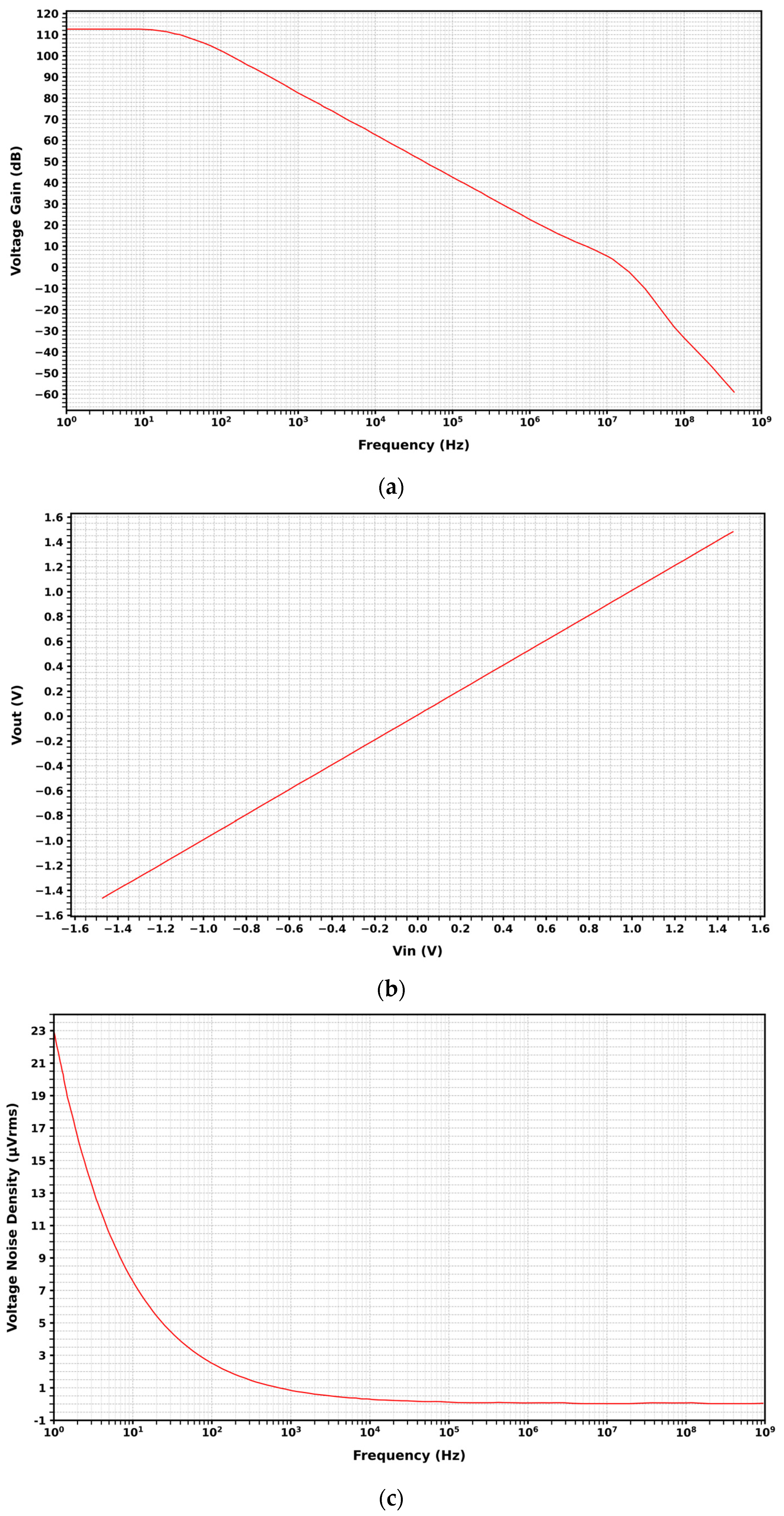
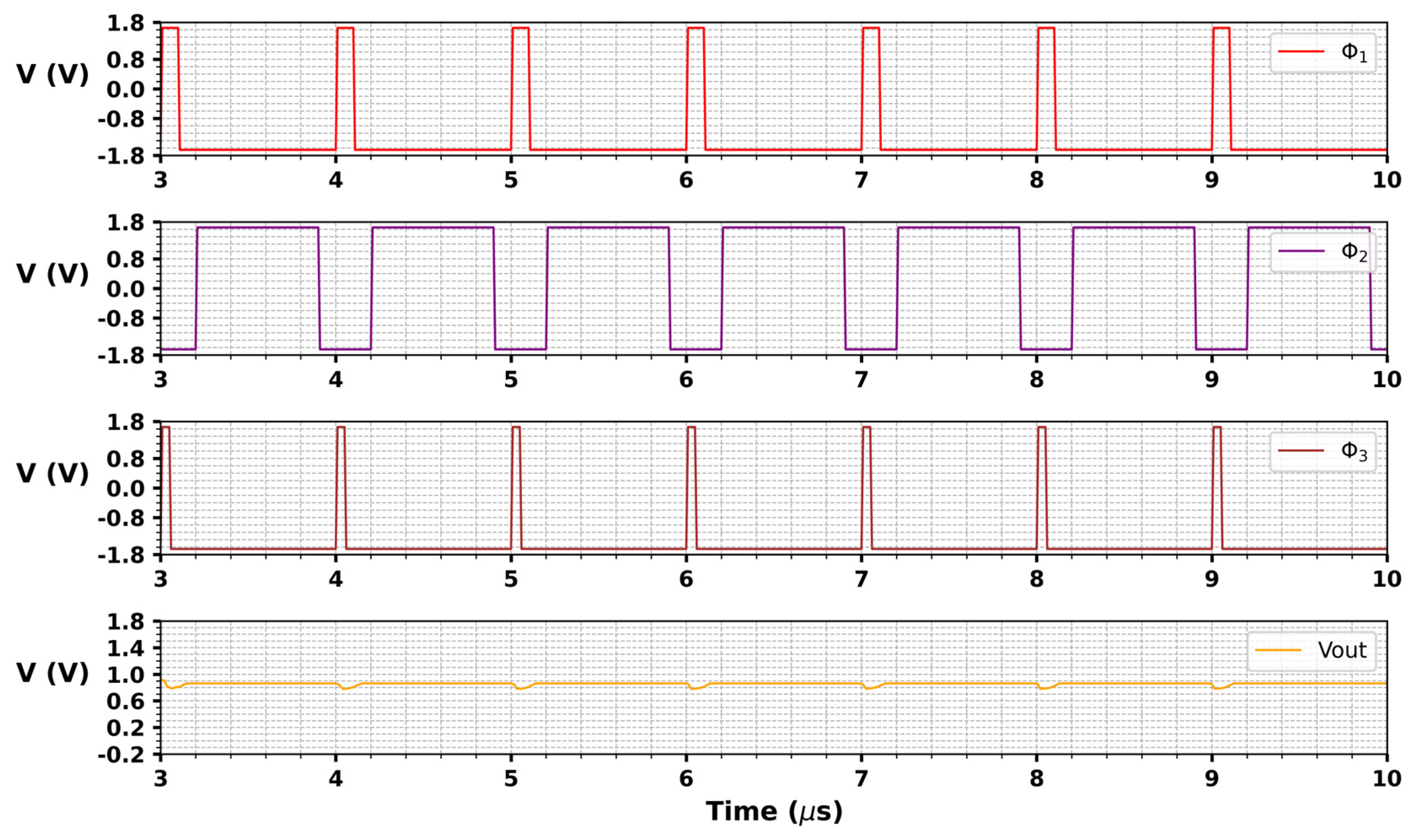
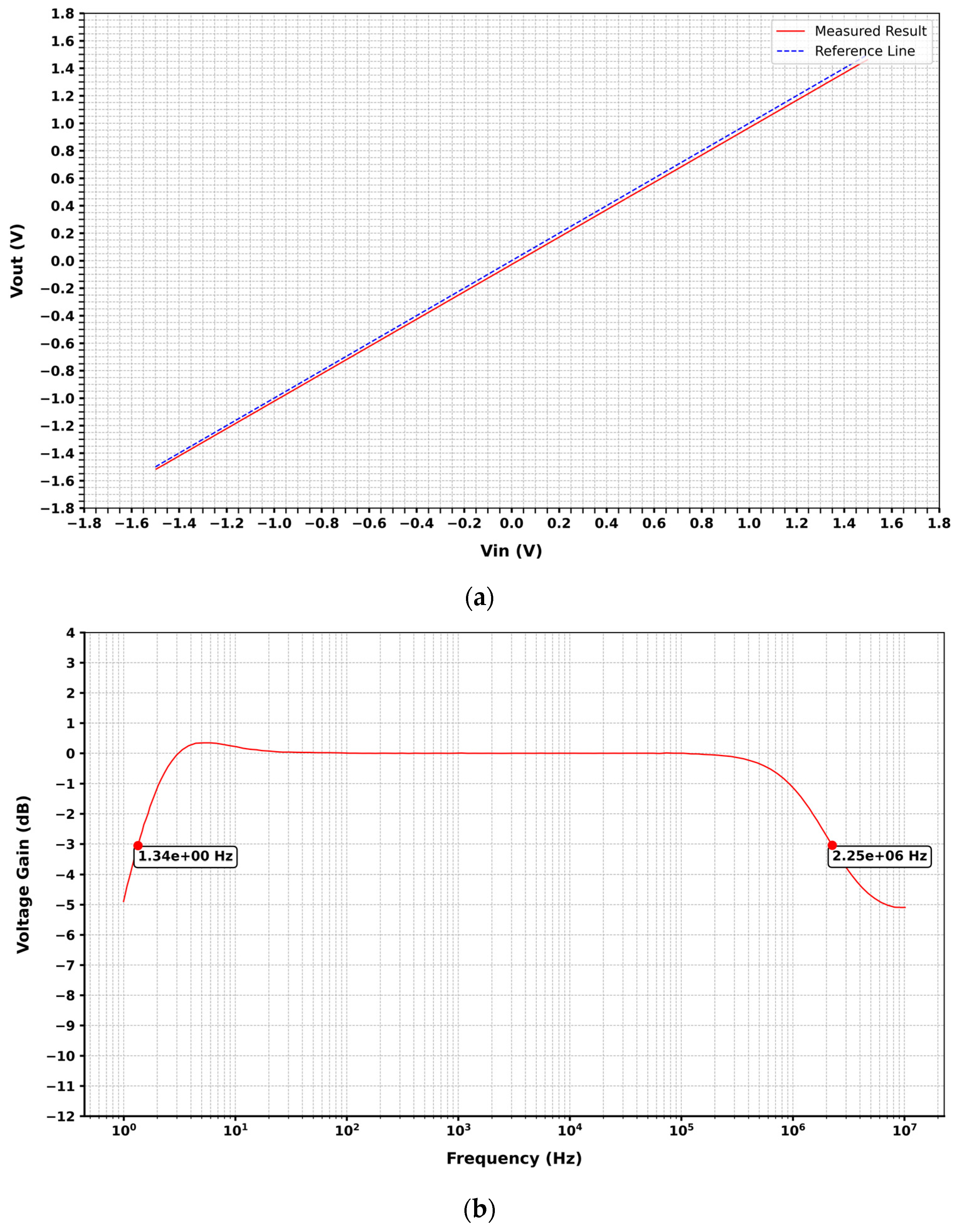
3. Results and Discussion

The proposed potentiometric readout circuit is fabricated in Magnachip 0.18 µm CMOS technology [42]. Cadence Virtuoso (Cadence Design Systems, San Jose, CA, USA) is employed to design the schematic and layout. The design rule check and post layout parasitic RC extraction are performed using Cadence Assura. Figure 6 shows the layout of full chip, where the proposed CDS with SC-LPF architecture is highlighted in yellow. The layout of the CDS with SC-LPF architecture occupies an area of 990 µm × 216 µm. The chip operates at a power supply of ±1.65 V. The utilized fabrication process supports six metal layers for an interconnection and pad with size of 67 μm × 67 μm. The post layout simulation is carried out by using a 1 MHz clock with a sampling capacitor of 1 pF and a load capacitor of 5 pF. The input voltage range used for the simulation is from −1.5 V to +1.5 V, which is the pH sensor output.
Figure 7 depicts the transient response of the CDS stage when an input voltage of 1 V is applied, with a 1 MHz sampling clock frequency and a load capacitance of 5 pF. The transient response of the designed CDS is shown when it is configured with unity gain. The X-axis of the graph represents the time in units of µs, and the Y-axis corresponds to the CDS stage output voltage in units of volts. It can be seen from Figure 7 that the output voltage of the CDS circuit follow the applied input voltage, indicating that CDS circuit is acting as a potentiometric readout. The settling time of CDS output voltage depends on the value of switched capacitor in the CDS.
The transient response of the designed CDS with SC-LPF is presented in Figure 8. For the simulation, an input voltage ( V i n ) of 1 V is applied with a sampling frequency of 1 MHz and 5 pF load capacitance, and the output voltage of the CDS with SC-LPF stage ( V o u t ) is measured. Three clocks (Φ1, Φ2, and Φ3) are used to simulate the proposed circuit, operating at 1 MHz frequency with a duty cycle ratio of 20%, 70%, and 5%, respectively. These clocks are intended to be supplied externally using a microcontroller.
The X-axis in Figure 8 represents the time in units of µs and the Y-axis is voltage in volts. As expected, V o u t of the CDS with SC-LPF stage is following the V i n , which behaves as the potentiometric readout. The glitches at V o u t is caused by the switching action of Φ3, that samples V o u t . Similarly, the transient response of CDS and CDS with SC-LPF are evaluated using additional input voltages, including 500 mV, −500 mV, −1 V, 1.5 V, and −1.5 V, for verification purposes.
Figure 9 illustrates the noise response of designed CDS stage and CDS followed by SC-LPF during the circuit simulation. To measure the noise, all the AC input voltages are set to ground potential, and the RMS noise is measured at the output of each stage. The X-axis of the graphs corresponds to frequency in Hz, while the Y-axis represents noise in V/ H z . The flicker noise dominates the thermal noise at lower frequencies, and the flicker noise gradually dies out, leaving a constant thermal noise at the higher frequencies. By integrating the noise over the frequency range of 10 Hz to 100 MHz, the RMS output noises of CDS circuit and CDS followed by SC-LPF are 1.49 µ V r m s and 0.70 µ V r m s , with a power consumption of 60 µW and 124 µW, respectively.
The post-extraction simulation is performed to measure overall DC swing of the proposed CDS with SC-LPF architecture, as captured in Figure 10a, where the X-axis and Y-axis represent V i n and V o u t in volts, respectively. In the simulation, V i n is swept in 50 mV steps from −1.5 V to +1.5 V, and the corresponding V o u t is measured. Figure 10a shows that the V o u t of the CDS with SC-LPF follows V i n ranged from −1.5 V to +1.5 V when a 1 MHz sampling clock and a 5 pF load are used. This demonstrates that the designed potentiometric readout circuit can linearly reproduce the pH sensor response in the range ±1.5 V. The figure further illustrates the deviation of the measured results from the ideal fitting line. Analysis of the linearity curve reveals that the error rate remains below 2.5% for the target DC swing. The overall frequency response of the CDS with SC-LPF system is shown in Figure 10b, which indicates a 3 dB pole frequency at 2.25 MHz. Here, the X-axis and Y-axis represent frequency in Hz and voltage gain in dB, respectively.
Table 2 presents a comparison of noise and power consumption from post layout simulation of all architectures that are discussed in this paper. The two-stage telescopic OPAMP architecture achieved a noise of 260.8 µ V r m s , which is significant. By implementing the CDS circuit with the OPAMP, the noise is reduced to a significantly lower value of 1.4 µ V r m s . The noise is further reduced to 0.683 µ V r m s by implementing the novel SC-LPF at the CDS output.
To comprehensively assess the system’s performance under varying environmental conditions, corner simulations are performed at temperatures of −40 °C, 27 °C, and 80 °C, covering a range of process variations SS, FF, FS, SF (slow–slow, fast–fast, fast–slow, slow–fast), and voltage fluctuations of ±1.55 V, ±1.65 V, and ±1.85 V. The results, including key metrics such as DC swing, noise performance, and power consumption for the different architectures, are summarized in Table 3, offering valuable insights into the system’s resilience under different operating scenarios.
A comparison of the proposed readout circuit with other existing architectures is summarized in Table 4. A switched-capacitor-based transimpedance amplifier, operating at a sampling frequency of 100 kHz with a 3 V supply, has been proposed for low noise and power consumption, where the input transistors are biased in the weak inversion region to minimize both power and noise [25]. However, the performance of transistors in the weak inversion region can be sensitive to fabrication process variations, which may lead to increased chip fabrication costs. In pH-sensing applications, recent potentiometric readouts that employ the constant voltage constant current (CVCC) method [24], low-noise DC-coupled sensor amplifiers [23], and dual-sensing CMOS arrays [27] exhibit high power consumption, rendering them unsuitable for in vivo applications. Many of the other architectures are characterized by high power consumption, large spatial requirements, and significant noise generation [26,28]. In contrast, the proposed readout circuit offers a superior balance of noise performance, power efficiency, and compactness, making it a more viable option for in vivo pH-sensing systems, as detailed in Table 4.

4. Conclusions

This work presents the design and implementation of a potentiometric readout circuit with CDS and SC-LPF for pH-sensing applications. The proposed circuit, fabricated in Magnachip 0.18 µm CMOS technology, operates with a ±1.65 V supply voltage and achieves a low noise performance of 0.683 µ V r m s . The design consists of two stages: the first stage, a CDS, and the second stage, an SC-LPF, operating at a 1 MHz clock frequency. The noise reduction from 260.8 µ V r m s in the OPAMP stage to 0.683 µ V r m s in the CDS with the SC-LPF demonstrates the effectiveness of the proposed architecture in mitigating noise, particularly at lower frequencies. The OPAMP used in the design is a two-stage telescopic architecture with a high gain of 110 dB, ensuring high performance for pH-sensing applications. Post-layout simulation results confirm that the circuit operates with a low power consumption of 124.1 µW while maintaining a linear response for the pH sensor’s DC output in the range of −1.5 V to +1.5 V. The compact design, measuring 990 µm × 216 µm, further demonstrates the suitability of the readout circuit for in vivo applications, such as oral healthcare devices that measure the pH of saliva using ISFET sensors. Overall, the proposed potentiometric readout circuit offers significant improvements in noise reduction, power efficiency, and area, making it a promising solution for accurate and low-power pH-sensing systems.

Author Contributions

Conceptualization, S.J. and R.P.; methodology, S.L. and R.P.; validation, S.L., R.P. and H.P.; formal analysis, H.P.; investigation, S.L. and R.P.; resources, S.J.; data curation, S.L. and H.P.; writing—original draft preparation, S.L.; writing—review and editing, H.P. and C.P.; visualization, S.J., C.P. and H.-J.C.; supervision, S.J. and H.-J.C.; project administration, S.J. and H.-J.C.; funding acquisition, S.J. and H.-J.C. All authors have read and agreed to the published version of the manuscript.

Funding

This research was supported by Kumoh National Institute of Technology (202103770001).

Data Availability Statement

The datasets generated from the current study are available from the corresponding author on reasonable request.

Conflicts of Interest

Revathy Perumalsamy was employed by the Sr. Staff ATE Engineer. The remaining authors declare that the research was conducted in the absence of any commercial or financial relationships that could be construed as a potential conflict of interest.

References

  1. Wencel, D.; Abel, T.; McDonagh, C. Optical Chemical PH Sensors. Anal. Chem. 2014, 86, 15–29. [Google Scholar] [CrossRef] [PubMed]
  2. Das, A.; Bhadri, P.; Beyette, F.R.; Jang, A.; Bishop, P.; Timmons, W. A Potentiometric Sensor System with Integrated Circuitry for in Situ Environmental Monitoring. In Proceedings of the 2006 Sixth IEEE Conference on Nanotechnology, Cincinnati, OH, USA, 17–20 July 2006. [Google Scholar]
  3. Pan, C.-W.; Chou, J.-C.; Sun, T.-P.; Hsiung, S.-K. Development of the Real-Time PH Sensing System for Array Sensors. Sens. Actuators B Chem. 2005, 108, 870–876. [Google Scholar] [CrossRef]
  4. Punjiya, M.; Rezaei, H.; Zeeshan, M.A.; Sonkusale, S. A Flexible PH Sensing Smart Bandage with Wireless CMOS Readout for Chronic Wound Monitoring. In Proceedings of the 2017 19th International Conference on Solid-State Sensors, Actuators and Microsystems (TRANSDUCERS), Kaohsiung, Taiwan, 18–22 June 2017. [Google Scholar]
  5. Punjiya, M.; Nejad, H.R.; Mostafalu, P.; Sonkusale, S. PH Sensing Threads with CMOS Readout for Smart Bandages. In Proceedings of the 2017 IEEE International Symposium on Circuits and Systems (ISCAS), Baltimore, MD, USA, 28–31 May 2017. [Google Scholar]
  6. Huang, X.; Yu, H.; Liu, X.; Jiang, Y.; Yan, M.; Wu, D. A Dual-Mode Large-Arrayed CMOS ISFET Sensor for Accurate and High-Throughput PH Sensing in Biomedical Diagnosis. IEEE Trans. Biomed. Eng. 2015, 62, 2224–2233. [Google Scholar] [CrossRef] [PubMed]
  7. Tamayol, A.; Akbari, M.; Zilberman, Y.; Comotto, M.; Lesha, E.; Serex, L.; Bagherifard, S.; Chen, Y.; Fu, G.; Ameri, S.K.; et al. PH-sensing Hydrogel Fibers: Flexible PH-sensing Hydrogel Fibers for Epidermal Applications (Adv. Healthcare Mater. 6/2016). Adv. Healthc. Mater. 2016, 5, 624. [Google Scholar] [CrossRef]
  8. Pourcielgouzy, M.; Assiesouleille, S.; Mazenq, L.; Launay, J.; Templeboyer, P. PH-ChemFET-Based Analysis Devices for the Bacterial Activity Monitoring. Sens. Actuators B Chem. 2008, 134, 339–344. [Google Scholar] [CrossRef]
  9. Ghoneim, M.T.; Nguyen, A.; Dereje, N.; Huang, J.; Moore, G.C.; Murzynowski, P.J.; Dagdeviren, C. Recent Progress in Electrochemical PH-Sensing Materials and Configurations for Biomedical Applications. Chem. Rev. 2019, 119, 5248–5297. [Google Scholar] [CrossRef]
  10. Baliga, S.; Muglikar, S.; Kale, R. Salivary PH: A Diagnostic Biomarker. J. Indian Soc. Periodontol. 2013, 17, 461. [Google Scholar] [CrossRef]
  11. Golan, R.; Gavrieli, I.; Lazar, B.; Ganor, J. The Determination of PH in Hypersaline Lakes with a Conventional Combination Glass Electrode. Limnol. Oceanogr. Methods 2014, 12, 810–815. [Google Scholar] [CrossRef]
  12. Veselinovic, D.; Velikic, Z. The PH Measurement with Glass Electrode in an Electromagnetic Field. J. Serb. Chem. Soc. 2016, 81, 1407–1414. [Google Scholar] [CrossRef]
  13. Anes, B.; Bettencourt da Silva, R.J.N.; Oliveira, C.; Camões, M.F. Seawater PH Measurements with a Combination Glass Electrode and High Ionic Strength TRIS-TRIS HCl Reference Buffers—An Uncertainty Evaluation Approach. Talanta 2019, 193, 118–122. [Google Scholar] [CrossRef]
  14. Chin, Y.-L.; Chou, J.-C.; Sun, T.-P.; Chung, W.-Y.; Hsiung, S.-K. A Novel PH Sensitive ISFET with on Chip Temperature Sensing Using CMOS Standard Process. Sens. Actuators B Chem. 2001, 76, 582–593. [Google Scholar] [CrossRef]
  15. Chung, W.-Y.; Lin, Y.-T.; Pijanowska, D.G.; Yang, C.-H.; Wang, M.-C.; Krzyskow, A.; Torbicz, W. New ISFET Interface Circuit Design with Temperature Compensation. Microelectronics 2006, 37, 1105–1114. [Google Scholar] [CrossRef]
  16. Bergveld, P. Thirty Years of ISFETOLOGY. Sens. Actuators B Chem. 2003, 88, 1–20. [Google Scholar] [CrossRef]
  17. Janata, J.; Josowicz, M. Organic Semiconductors in Potentiometric Gas Sensors. J. Solid State Electrochem. 2009, 13, 41–49. [Google Scholar] [CrossRef]
  18. Abdullah, M.F.; Adnan, M.A.; Aziz, M.G.A.; Hussein, Z.; Noor, M.H.M.; Azman, K.A.; Madzhi, N.K. A Comparative Study on Low Noise Precision Difet Operational Amplifier and Low Noise Operational Amplifier for Potentiometric Transduction Circuit. In Proceedings of the 2013 IEEE Business Engineering and Industrial Applications Colloquium (BEIAC), Langkawi, Malaysia, 7–9 April 2013. [Google Scholar]
  19. Bembnowicz, P.; Yang, G.-Z.; Anastasova, S.; Spehar-Deleze, A.-M.; Vadgama, P. Wearable Electronic Sensor for Potentiometric and Amperometric Measurements. In Proceedings of the 2013 IEEE International Conference on Body Sensor Networks, Cambridge, MA, USA, 6–9 May 2013. [Google Scholar]
  20. Adimulam, M.K.; Divya, A.; Tejaswi, K.; Srinivas, M.B. A Low Power, Low Noise Programmable Analog Front End (PAFE) for Biopotential Measurements. In Proceedings of the 2017 39th Annual International Conference of the IEEE Engineering in Medicine and Biology Society (EMBC), Jeju, Republic of Korea, 11–15 July 2017. [Google Scholar]
  21. Farouk, T.; Elkhatib, M.; Dessouky, M. A 1V Low-Power Low-Noise Biopotential Amplifier Based on Flipped Voltage Follower. In Proceedings of the 2015 IEEE International Conference on Electronics, Circuits, and Systems (ICECS), Cairo, Egypt, 6–9 December 2015. [Google Scholar]
  22. Park, H.; Lakshminarayana, S.; Pan, C.; Chung, H.-J.; Jung, S. An Auto Adjustable Transimpedance Readout System for Wearable Healthcare Devices. Electronics 2022, 11, 1181. [Google Scholar] [CrossRef]
  23. Krishnamurthy, H.K.; Robinson, D.; Rector, D.M.; La Rue, G.S. A Low Noise Low Power DC Coupled Sensor Amplifier with Offset Cancellation. In Proceedings of the 2010 IEEE Workshop on Microelectronics and Electron Devices, Boise, ID, USA, 16 April 2010. [Google Scholar]
  24. Chung, W.-Y.; Silverio, A.A.; Tsai, V.F.S.; Cheng, C.; Chang, S.-Y.; Zhou, M.-Y.; Kao, C.-Y.; Rustia, D.A.; Lo, Y.-W. Design of a Multi-Sensor Readout Chip for Amperometric, Potentiometric, Impedometric, and Colorimetric Bio-Sensor Applications. In Proceedings of the 2017 International Conference on Applied System Innovation (ICASI), Sapporo, Japan, 13–17 May 2017. [Google Scholar]
  25. Dubey, D.; Gupta, A. A Low Power Low Noise Amplifier for Biomedical Applications. In Proceedings of the 2015 IEEE International Conference on Electrical, Computer and Communication Technologies (ICECCT), Coimbatore, India, 5–7 March 2015. [Google Scholar]
  26. Kuo, P.-Y.; Chen, Y.-Y. A Novel Low Unity-Gain Frequency and Low Power Consumption Instrumentation Amplifier Design for RuO2 Uric Acid Biosensor Measurement. IEEE Trans. Instrum. Meas. 2021, 70, 4003409. [Google Scholar] [CrossRef]
  27. Wang, Z.; Keeble, L.; Moser, N.; Lande, T.S.; Georgiou, P. A Dual-Sensing CMOS Array for Combined Impedance-PH Detection of DNA with Integrated Electric Field Manipulation. In Proceedings of the 2021 IEEE International Symposium on Circuits and Systems (ISCAS), Daegu, Republic of Korea, 22–28 May 2021. [Google Scholar]
  28. Silverio, A.A.; Chung, W.-Y.; Tsai, V.F.S.; Cheng, C. Multi-Parameter Readout Chip for Interfacing with Amperometric, Potentiometric and Impedometric Sensors for Wearable and Point-of-Care Test Applications. Microelectronics 2020, 100, 104769. [Google Scholar] [CrossRef]
  29. Taheri, H.E.; Mirhassani, M. A Low-Power, High-Resolution, Adaptive Sensitivity Readout Circuit with Selective Detection Range for Capacitive Biosensors. Int. J. Electron. Commun. 2021, 131, 153599. [Google Scholar] [CrossRef]
  30. Springer, E.K. PH Measurement Guide. Available online: https://separations.co.za/wp-content/uploads/2014/09/pH-Measurement-Guide.pdf (accessed on 27 June 2024).
  31. Available online: https://www.ti.com/lit/an/snoa529a/snoa529a.pdf?ts=1652094714270 (accessed on 27 June 2024).
  32. Available online: https://www.hamiltoncompany.com/process-analytics/ph-and-orp-knowledge/ph-probe-operation-principles/slope-of-ph-sensor (accessed on 27 June 2024).
  33. Yan, L.; Georgiou, P.; Constandinou, T.G.; Garner, D.; Toumazou, C. An Auto-Offset-Removal Circuit for Chemical Sensing Based on the PG-ISFET. In Proceedings of the 2009 IEEE International Symposium on Circuits and Systems, Taipei, China, 24–27 May 2009. [Google Scholar]
  34. Liu, Y.; Toumazou, C. An ISFET Based Sensing Array with Sensor Offset Compensation and PH Sensitivity Enhancement. In Proceedings of the Proceedings of 2010 IEEE International Symposium on Circuits and Systems, Paris, France, 30 May–2 June 2010. [Google Scholar]
  35. Chen, M.-C.; Chen, H.-Y.; Lin, C.-Y.; Tsai, C.-M.; Hsieh, C.-F.; Horng, J.-T.; Qiu, J.-T.; Huang, C.-C.; Yang, F.-L. A Novel Smart Nanowire Biosensor with Hybrid Sensor/Memory/CMOS Technology. In Proceedings of the 2010 International Electron Devices Meeting, San Francisco, CA, USA, 6–8 December 2010. [Google Scholar]
  36. Lee, T.-H.; Cho, G.; Kim, H.J.; Lee, S.W.; Lee, W.; Han, S.H. Analysis of 1/f Noise in CMOS Preamplifier with CDS Circuit. IEEE Trans. Nucl. Sci. 2002, 49, 1819–1823. [Google Scholar] [CrossRef]
  37. Belloni, M.; Bonizzoni, E.; Fornasari, A.; Maloberti, F. A Micropower Chopper—CDS Operational Amplifier. IEEE J. Solid-State Circuits 2010, 45, 2521–2529. [Google Scholar] [CrossRef]
  38. Enz, C.C.; Temes, G.C. Circuit Techniques for Reducing the Effects of Op-Amp Imperfections: Autozeroing, Correlated Double Sampling, and Chopper Stabilization. Proc. IEEE Inst. Electr. Electron. Eng. 1996, 84, 1584–1614. [Google Scholar] [CrossRef]
  39. Gray, P.R.; Hurst, P.J.; Lewis, S.H.; Meyer, R.G. Analysis and Design of Analog Integrated Circuits, 6th ed.; John Wiley & Sons: Nashville, TN, USA, 2024; ISBN 9781394220069. [Google Scholar]
  40. Carusone, T.C.; Johns, D.A.; Martin, K.W. Analog Integrated Circuit Design: International Student Version, 2nd ed.; John Wiley & Sons: Nashville, TN, USA, 2012; ISBN 9781118092330. [Google Scholar]
  41. Razavi, B. Design of Analog CMOS Integrated Circuits, 2nd ed.; McGraw-Hill Education: Columbus, OH, USA, 2016; ISBN 9781259255090. [Google Scholar]
  42. Available online: https://www.magnachip.com/magnachip-offers-automotive-grade-0-18-micron-bcd-process-technology-with-up-to-200v-operation-voltage/ (accessed on 6 January 2025).
  43. Prathap, V.; Titus, A.H. ISFET Pixel Array with Selectable Sensitivity and Bulk-Based Offset-Drift Nullification Capability for Reduction of Non-Ideality Effects. IEEE Sens. J. 2023, 23, 1827–1836. [Google Scholar] [CrossRef]
  44. Duan, M.; Zhong, X.; Zhao, X.; El-Agnaf, O.M.; Lee, Y.-K.; Bermak, A. An Optical and Temperature Assisted CMOS ISFET Sensor Array for Robust E. Coli Detection. IEEE Trans. Biomed. Circuits Syst. 2021, 15, 497–508. [Google Scholar] [CrossRef] [PubMed]
  45. Zeng, J.; Kuang, L.; Cacho-Soblechero, M.; Georgiou, P. An Ultra-High Frame Rate Ion Imaging Platform Using ISFET Arrays with Real-Time Compression. IEEE Trans. Biomed. Circuits Syst. 2021, 15, 820–833. [Google Scholar] [CrossRef]
Figure 1. Implementation of the CDS circuit.
Jlpea 15 00003 g001
Figure 2. (a) Implementation of the resistor emulator for input sampling stage; (b) implementation of the resistor emulator for feedback stage.
Jlpea 15 00003 g002
Figure 3. Telescopic OPAMP architecture.
Jlpea 15 00003 g003
Figure 4. (a) AC response of OPAMP, voltage gain (dB) versus frequency (Hz); (b) DC response of OPAMP, V i n (V) versus V o u t ( V ) ; (c) Noise analysis of OPAMP, noise (µ V r m s ) versus frequency (Hz).
Jlpea 15 00003 g004
Figure 5. Design of CDS circuit with SC-LPF.
Jlpea 15 00003 g005
Figure 6. Full chip layout highlighting the proposed CDS with SC-LPF architecture.
Jlpea 15 00003 g006
Figure 7. Transient response at the CDS output for input voltage of 1 V with 1 MHz clock and 5 pF load.
Jlpea 15 00003 g007
Figure 8. Transient response at the CDS and SC-LPF output for input voltage of 1 V with 1 MHz clock and 5 pF load.
Jlpea 15 00003 g008
Figure 9. Output noise performance of CDS and CDS with SC-LPF at pre-layout circuit simulation, noise ( V r m s ) versus frequency (Hz).
Jlpea 15 00003 g009
Figure 10. Post extraction simulation of the overall system (a) V i n versus V o u t linearity plot; (b) frequency response.
Jlpea 15 00003 g010
Table 1. List of important abbreviations and symbols.
SymbolAbbreviation
CDSCorrelated double sampler
SC-LPFSwitched-capacitor low-pass filter
S n t o t a l f OPAMP noise spectral density
V i n 2 Input voltage noise
V c d s 2 Output noise of CDS
V s c _ l p f 2 Output noise of CDS with SC-LPF
H c d s ( f ) Transfer function of CDS
H s c _ l p f ( f ) Transfer function of CDS with SC-LPF
f 1 Cutoff frequency of CDS
f 2 S C _ L P F Cutoff frequency of CDS with SC-LPF
V i n Input voltage of overall system
V o u t Output voltage of overall system
R i n Input resistor
R f Feedback resistor
Table 2. Post layout simulation results of various architectures.
ParameterOPAMPCDSCDS with SC-LPF
Output noise ( V r m s ) 260.8 µ1.4 µ0.683 µ
Power consumption (Watt)44.1 µ70.7 µ124.1 µ
Table 3. Post layout corner simulation results.
ParameterTemperature (°C)Corner FrequencySupply Voltage (V)
−402780SSFFFSSF−1.55 to +1.55−1.65 to +1.65−1.85 to +1.85
Opamp DC swing (V)−1.5 to +1.49−1.5 to +1.47−1.5 to +1.5−1.5 to +1.49−1.5 to +1.48−1.5 to +1.5−1.5 to +1.5−1.5 to +1.49−1.5 to +1.48−1.5 to +1.5
Opamp noise ( µ V r m s )236.8260.8282.5308.8200.9296.6246290.7260.8207.1
Opamp power (µW)24.3244.161.1319.7183.633.2956.725.1444.185.65
CDS DC swing (V)−1.5 to +1.5−1.5 to +1.5−1.5 to +1.5−1.5 to +1.5−1.5 to +1.5−1.5 to +1.5−1.5 to +1.5−1.5 to +1.5−1.5 to +1.5−1.5 to +1.5
CDS noise ( µ V r m s ) 1.451.41.871.21.231.221.211.291.391.41
CDS power (µW)40.1570.796.832.6130.453.790.640.670.7135.3
CDS with SC-LPF DC swing (V)−1.5 to +1.5−1.5 to +1.5−1.5 to +1.5−1.5 to +1.5−1.5 to +1.5−1.5 to +1.5−1.5 to +1.5−1.5 to +1.5−1.5 to +1.5−1.5 to +1.5
CDS with SC-LPF noise ( µ V r m s ) 0.560.680.770.700.670.670.690.670.680.74
CDS with SC-LPF power (µW)71.15124.1170.7357.2223294.9159.172124286.34
Table 4. Architecture comparison of proposed readout circuit with existing methodologies.
RefPower (Watt) Noise   ( V r m s ) Area (mm2)Supply (V)Technology (µm)Application
[23]900 µ991.1 µN/A1CMOS 0.18pH sensing
[24]1.67 mN/AN/A3.3 & 1.8CMOS 0.18pH sensing
[25]15.17 µ2.89 µN/A3CMOS 0.18ECG
[26]397.92 µN/A0.441.5CMOS 0.18Uric acid sensing
[27]3.43 m114 µ0.311.8CMOS 0.18pH sensing
[28]1.67 mN/A1.441.8CMOS 0.18Multi-purpose
[29]6.6 μ26.89 μN/A1.8CMOS 0.18Capacitive sensing
[43]3 m1.22 m43.3CMOS 0.35pH sensing
[44]7.98 m6.57 m3.43.3 & 1.8CMOS 0.18pH sensing
[45]240 mN/A41.8CMOS 0.18pH sensing
This work124.1 µ0.683 µ0.21 ±1.65CMOS 0.18pH sensing
Disclaimer/Publisher’s Note: The statements, opinions and data contained in all publications are solely those of the individual author(s) and contributor(s) and not of MDPI and/or the editor(s). MDPI and/or the editor(s) disclaim responsibility for any injury to people or property resulting from any ideas, methods, instructions or products referred to in the content.

