Abstract
In this paper, a new technique for improvement on the DC voltage gain, while keeping the high-linearity in symmetrical operational transconductance amplifier (OTA) bulk-driven (BD) topology is proposed. These features are achieved by allying two topological solutions: enhanced forward-body-biasing self-cascode current mirror, and source degeneration. The proposed concept is demonstrated through simulations with typical process parameters and Monte Carlo analysis on nominal transistors of the CMOS TSMC 180 nm node. Results indicate that the proposed OTA can achieve a very small transconductance, only 542 pA/V while keeping a voltage gain higher than 60 dB, 150 dB CMRR, and high linearity of 475 mVpp (1% THD), consuming only 1.9 nW for a supply voltage of 0.6 V. This set of features allows the proposed OTA to be an attractive solution for implementing OTA-C filters for the analog front-ends in wearable devices and bio-sensing.
1. Introduction
The effort to develop implantable or bio-sensing battery-less biomedical instrumentation systems has been continuously challenging analog designers because of the intensified constraints arising from CMOS scaling [1,2,3]. Topological solutions for endowing operational transconductance amplifiers (OTAs) to process μV signals with common-mode swings in the range of tens of volts, allied to features like ultra-low power consumption, low-noise, enhanced linearity, high common-mode rejection ratio (CMRR), tiny silicon footprint, and large common-mode range (CMR) are frequently pursued by the analog circuit designers [4,5,6,7,8,9,10,11,12,13,14,15,16,17,18].
As a basic block in analog front-ends (AFEs) for biosensing, the OTA-C filter with large time constants is among the most important applications for OTAs with reduced transconductance [19]. Such circuits when used in implantable/wearable biomedical applications have their design challenged by the restricted-sized on-chip integrated capacitors. In order to decrease the size of such filters, OTAs must output a very small transconductance in the order of a few nA/V, which is achieved with very low biasing currents [20] at the cost of the OTA linearity.
Among the typical OTA design techniques to increase linearity is the use of non-unity gain current mirrors [21,22,23] to allow higher biasing currents and maintain a low transconductance. Another well-known technique that is used to improve both OTA linearity and input signal voltage swing is the bulk-driven differential pair [1,24,25,26,27,28,29]. Unlike the gate-driven OTA topologies, the bulk-driven OTAs outputs are an alternative for a relatively lower transconductance [20,30]. In this case, the main drawback of this approach is a poor DC voltage gain, which can be improved by using several techniques [25]. An interesting and widely employed technique relies on a self-cascode topology known as trapezoidal or composite transistor [31,32,33,34]. Additionally, an improvement for the self-cascode transistor association was proposed in [13,35,36,37] allowing to increase voltage gain and decrease area usage. Therefore, in this paper, we propose a new symmetrical bulk-driven OTA topology that takes the advantages of previously described techniques, i.e., the combination of the topology presented by [23], with a bulk-driven differential pair [24], and the bulk-driven active source degeneration linearization technique adapted from [1,38]. Besides the employed combination of techniques in the OTA topology, we propose an innovative improved self-cascode current mirror (ISCCM) which is based on [35,37].
This paper is organized as follows: Section 2 describes current mirror topologies made of rectangular transistor arrays (composite transistor). The improved self-cascode current mirror that sources the proposed OTA is introduced. Section 3 presents the bulk-driven symmetrical OTAs topologies. Simulations and comparisons among the proposed BD topology, the conventional bulk-driven, and state-of-art transconductors are shown in Section 4. Finally, Section 5 presents the conclusions.
2. Current Mirrors
Current mirrors are the essential component of CMOS OTAs, and their output impedance improvement leads to OTAs with superior voltage gain and common-mode rejection. Implementing current mirrors with series-parallel associations of transistors is a design solution that allows for high current gain, reduced area usage, and less process variability compared to parallel-only current mirrors [22]. This technique was employed by [23] to achieve very low transconductance OTAs without sacrificing linearity and process variability tolerance [13,14]. Since the output transistor array has a large equivalent channel length (), the output current is less dependent on the output voltage variation.
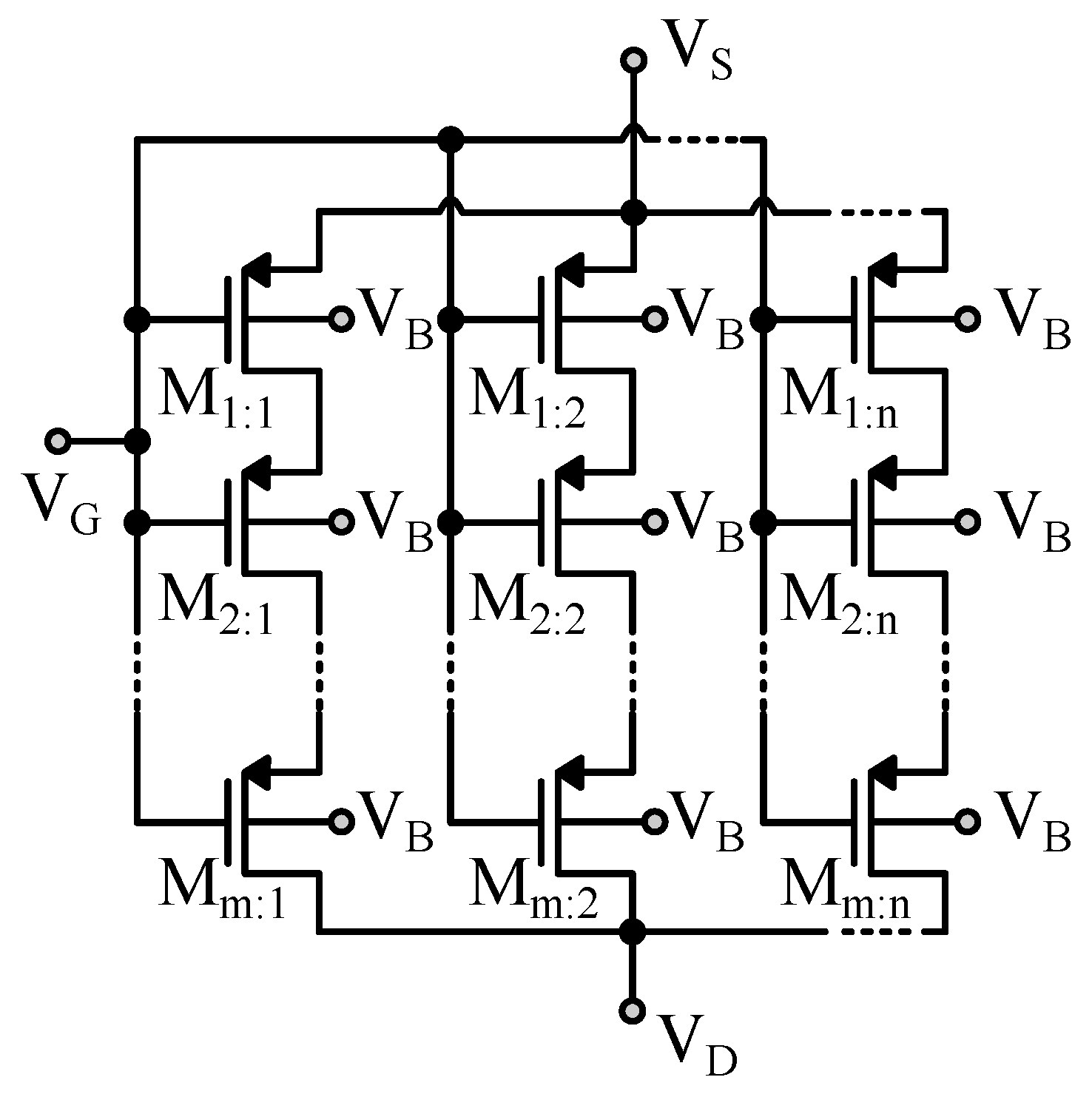
Rectangular transistor arrays as illustrated in Figure 1 can be considered understood as a single transistor [31] with a higher output impedance [2,23,39]. The rectangular array, shown in Figure 1, is an m by n matrix of single transistors composed of m parallel columns of n series single transistors. The rectangular equivalent transistor aspect ratio is a function of the single transistor aspect ratio , as shown in Equation (1). The total gate area of the rectangular array is , where is the gate area of the single transistor.

Figure 1.
Rectangular transistor array.
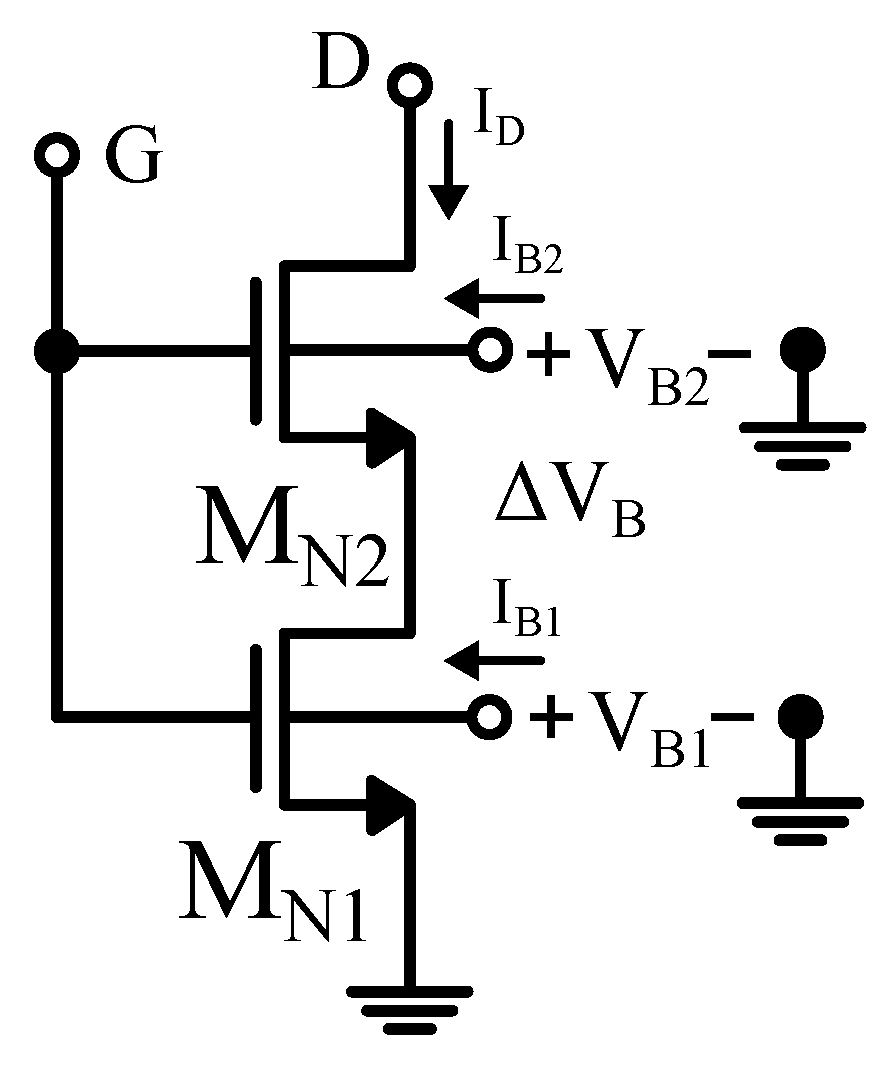
Figure 2 represents an N-type improved composite transistor. It consists of a series connection of two independently forward-body-biased N-type MOS transistors MN1 and MN2, as first proposed in [35], and described in detail in [13,14,37], by using the ACM (advanced compact model) all-region transistor model [40].

Figure 2.
Improved composite transistor.
The improved composite transistor equivalent aspect ratio is defined as:
where
represents a correction factor for the current drain I definition due to the difference between the body-bias of the series transistors MN2 and MN1 , assuming the transistors are operating in weak inversion, and
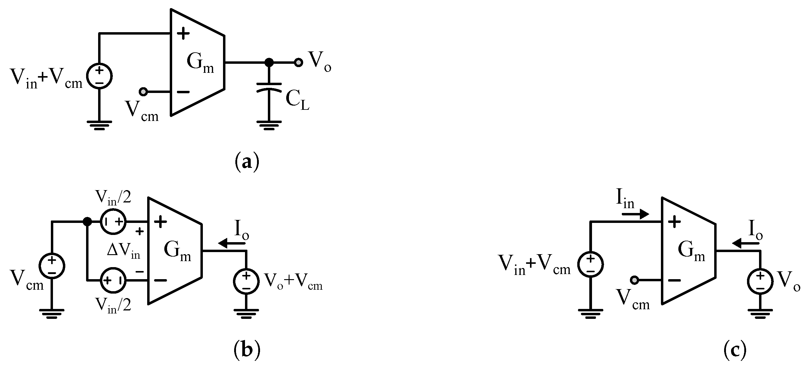
is the ratio between transistors MN1 and MN2 and physical aspect ratios and . Figure 3a shows the conventional current mirror (CM). The ratio between transistors M, and M aspect ratios and define the current mirror gain and attenuation . In order to have a better matching for non-unity current gain, the current mirror transistors should be replaced with rectangular transistor arrays [22].
A higher current attenuation is achieved by combining parallel transistor arrays at the current mirror input, and series transistor arrays at the output. This scheme is a desirable feature for ultra-low transconductance OTAs [21,23], as it provides transconductance attenuation without decreasing linearity.
The typical cascode current mirror is a variation of the Wilson current mirror first proposed by [41]. The topology increases the output impedance in order to decrease the output current gain error. On the other hand, its drawback is a lower output voltage swing, which will be solved by the proposed current mirror as follows.
An alternative topology to a typical cascode, is the self-biased self-cascode current mirror (SCCM), first proposed by [42], which uses composite transistor arrays in a trapezoidal shape, which are equivalent to single transistors with increased output impedance. The trapezoidal geometry means that the top composite transistors, i.e., those related to drain portion must have a greater aspect ratio than the bottom transistors, i.e., corresponding to source portion, so this kind of composite transistor can be made by arranging their drain transistors in an array connected to a series array corresponding to source transistors (the smaller base of the trapezoid) [43]. This topology is recommended for low input currents and unity current mirror gain, but it is not appropriate for higher currents or very large current gains, since it would require a very large area. Nevertheless, the trapezoidal current mirror can still use the parallel-series technique for current attenuation [21,22] by replacing the output series transistor array with a trapezoidal transistor array, as shown in Figure 3b. This is possible because there is no need for trapezoidal arrays at the mirror input for non-unity gains.

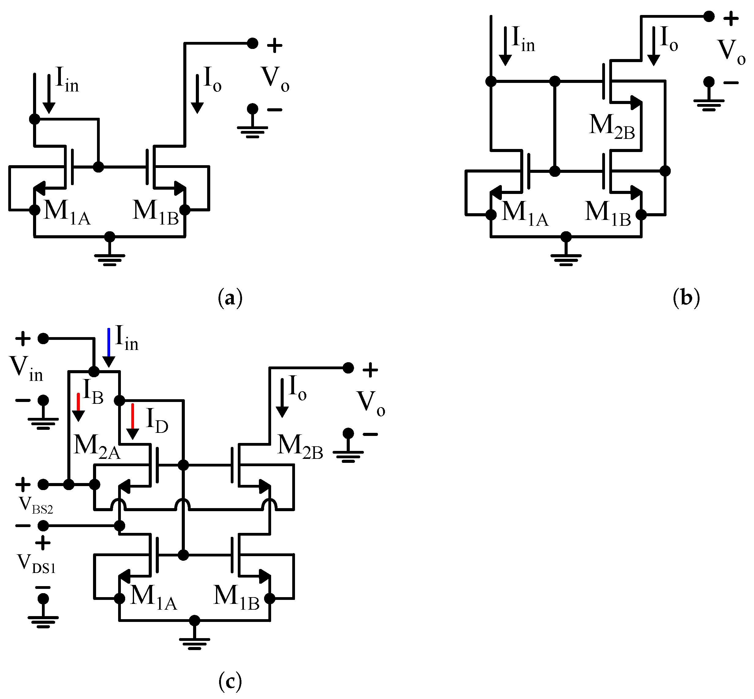
Figure 3.
Self-biased current mirrors: (a) conventional current mirror with rectangular transistor arrays (CM) [22], (b) trapezoidal output current mirror (SCCM) [42], and (c) improved self-cascode current mirror (ISCCM).
Figure 3.
Self-biased current mirrors: (a) conventional current mirror with rectangular transistor arrays (CM) [22], (b) trapezoidal output current mirror (SCCM) [42], and (c) improved self-cascode current mirror (ISCCM).
By taking (2), , and since M and M bulk terminals are connected to each other, the current gain can be expressed as
For , the SCCM current gain is approximately , as in the conventional parallel-series current mirror. However, this current mirror has a relatively larger output resistance, consequently, it is more tolerant to output voltage variation.
The SCCM output resistance can be further increased by independently forward-body-biasing transistors M and M by connecting their shared gate terminals to their shared bulk-terminals [37], as shown in Figure 3c. In its turn, the k factor is increased by a factor function of the bulk-to-source voltage , accordingly to (3), and hence the gain of the current mirror, is defined as
Again, considering a high value of , the current gain is approximately .
For proof of concept, the above current mirrors were designed for the TSMC 180 nm technology and simulated for typical process parameters and room temperature. Table 1 summarizes the transistor arrays dimensions for each circuit.

Table 1.
Transistor sizes (Figure 3).
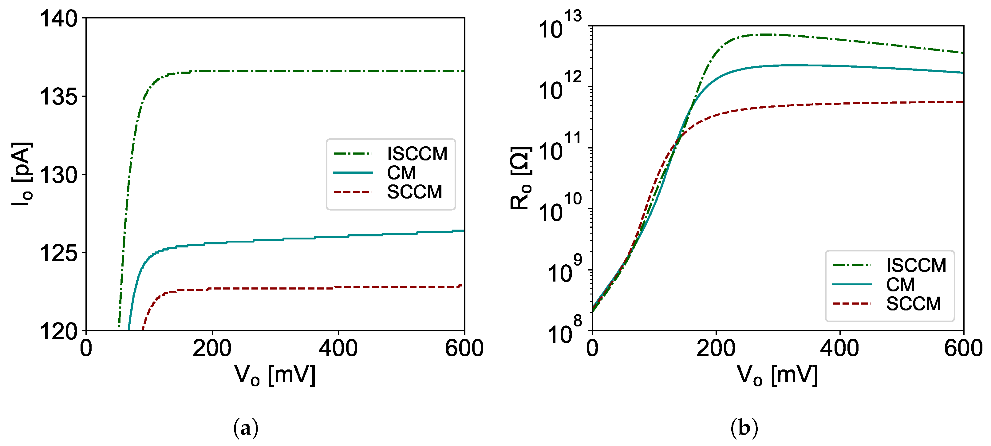
First, by considering a fixed 1.6 nA input current I and an output voltage sweeping from 0 to 600 mV, Figure 4a shows the output current mirrors. According to the transistor arrays dimensions, the conventional rectangular parallel-series current mirror (CM) should attenuate the input current by a 16× factor, and provide a 100 pA current. However, due to non-ideal behavior, it outputs about 125 nA, which is close to 13× attenuation. The self-cascode current mirror (SCCM) behaves similarly to CM, as . The improved self-cascode current mirror (ISCCM) has a slightly smaller attenuation, close to 12×. The main difference between these current mirrors is the output resistance , shown in Figure 4b. At the saturation region, the SCCM is much higher than CM, while the ISCCM is more than one order of magnitude higher.
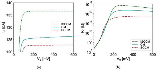
Figure 4.
Current mirrors comparison: (a) output current × output voltage, and (b) output resistance × output voltage for Iin = 1.6 nA.
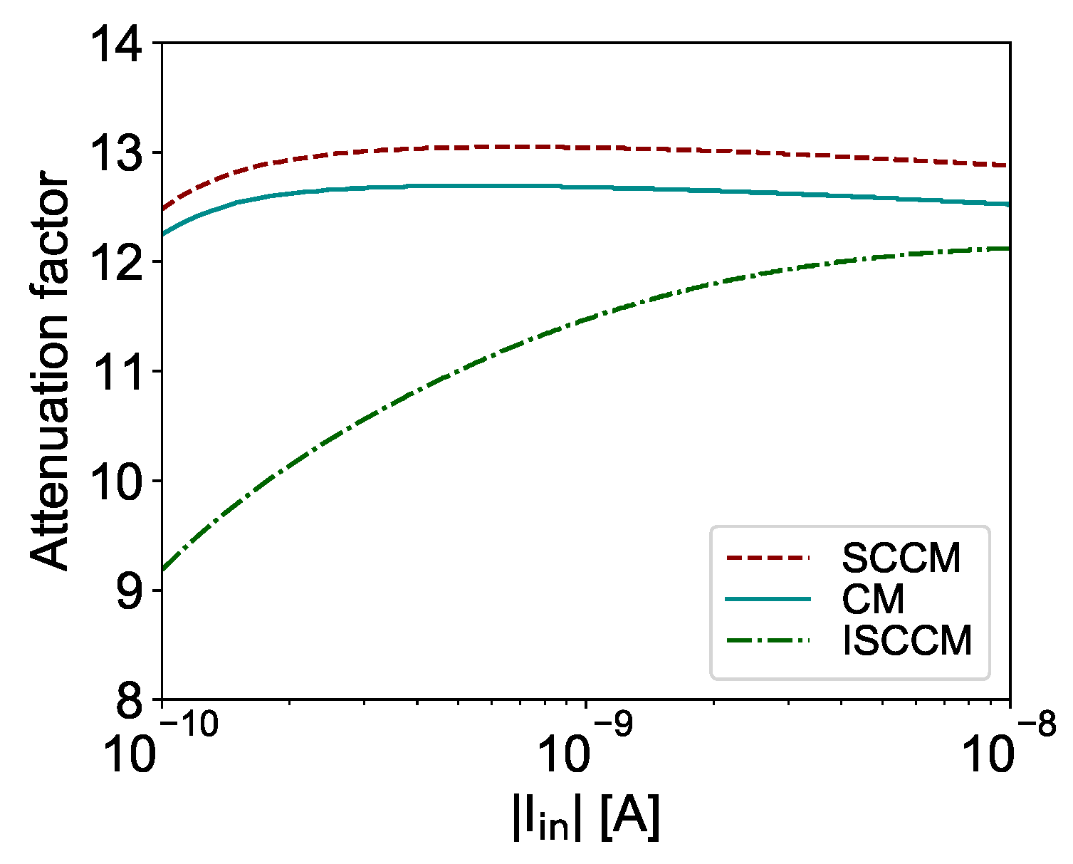
Nonetheless, the ISCCM is not perfect. Figure 5 shows the current attenuation as a function of the input current I. As can be seen, the current attenuation is practically constant for the CM and SCCM, but it varies for the ISCCM, as the is indirectly a function of the input current.
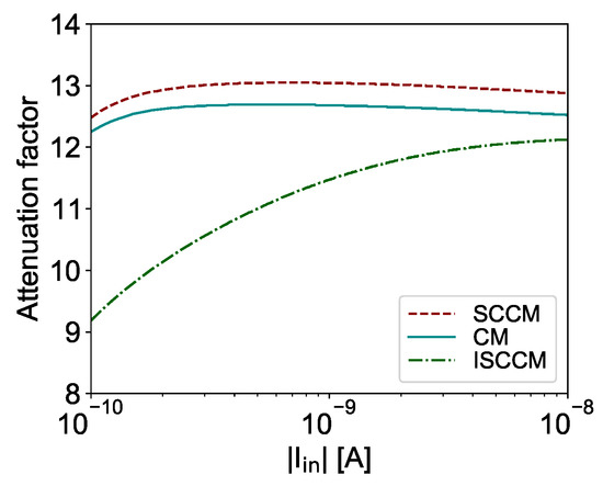
Figure 5.
Current mirrors attenuation as a function of input current for = 0.3 V.
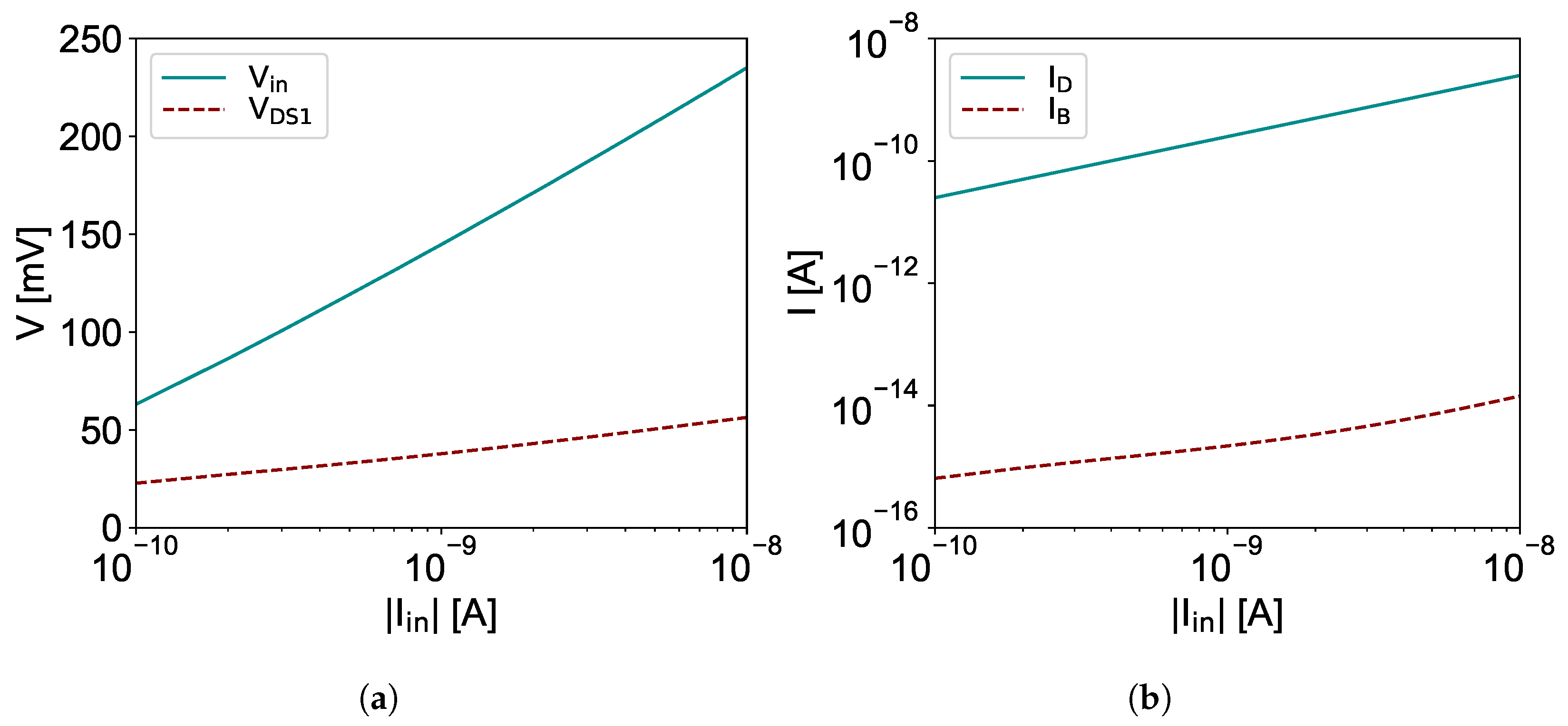
The ISCCM differential bulk voltage is defined as . As the input current I increases exponentially, increases linearly, as shown in Figure 6a. For 1 nA input, is approximately 100 mV. As is always positive, the transistors M and M are forward-body-biased. In spite of that, the drain current I is orders of magnitude higher than I (see Figure 6b), so I ≈ I.
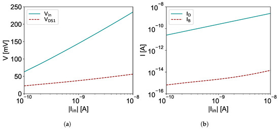
Figure 6.
Improved self-cascode current mirror: (a) Vin and VDS1 voltages × input current, and (b) drain (ID) and bulk currents (IB) × input current.
3. Bulk-Driven Symmetrical Operational Transconductance Amplifiers
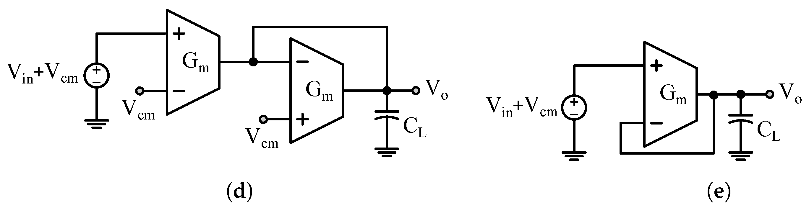
Bulk-driven OTA topologies as illustrated in Figure 7 take advantage of the transistor bulk terminal of the differential pair to achieve higher transconductance linearity and input range rather than conventional gate-driven topologies [25,28].
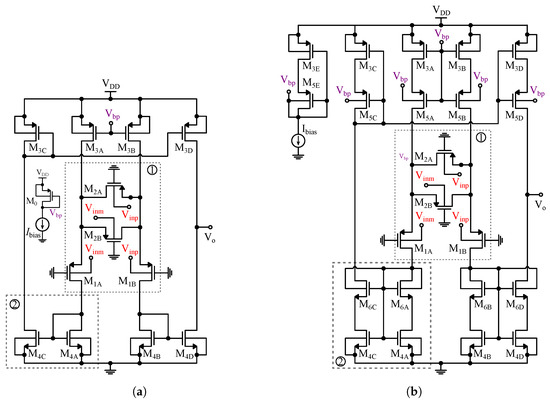
Figure 7.
Symmetrical OTA topologies: (a) with parallel-series current mirrors [21], bulk-driven inputs and active source degeneration [1,38], and (b) proposed topology with the addition of improved current mirrors.
The intrinsic drawback of this scheme is the reduced transconductance due to its equivalent gate-driven OTA, hence, a lower DC voltage gain. Nonetheless, biomedical applications frequently involve slow varying quantities and the supposed disadvantage, i.e., the very-low transconductance turns beneficial as analog signal filters with very low cut-off frequencies using relatively small-sized integrated capacitors are essential. Moreover, the lower voltage gain can be addressed with techniques such as positive feedback [25], cascode gain stages [44], and transistor arrays [31,45].
Figure 7b shows the proposed topology which relies on the conventional symmetrical OTA shown in Figure 7a with a key aspect. The current mirrors are built by improved self-cascode configuration [36], according to Figure 3c. This scheme allows increasing the OTA DC voltage gain as also the CMRR. Further, in this work, the conventional BD-OTA (see Figure 7b) makes use of the same active source degeneration technique [1,38,46] employed in the input differential pair to keep fair comparisons between the topologies.
To describe the topology behavior, we use the ACM transistor model (more details in [47]), hence the BD-OTA topology can be explained as follows: the transconductance is a function of the differential pair transconductance , the source degeneration factor a [46], and the current mirror factor N, as defined by (7). The differential pair transconductance , defined by (8) and is attenuated relative to the gate-driven OTA by a factor of .
Another advantage of the bulk-driven topology over the gate-driven approach is the reduced minimum supply voltage needed for operation, since the differential pair transistors M and source degeneration transistors M gate terminals are connected to the ground instead of to the input signal voltages, which has a typical common-mode voltage of half the supply voltage. It is worth noting that, in order to M operate in the saturation region, should be greater than the sum of and , which is achieved by assuring that is sufficiently greater than [38,46].
The differential pair is composed of the transistors M, and the active source degeneration transistors M. The ratio between the differential pair and the source degeneration transistor aspect ratios is 4 for the earlier explained reasons and is achieved by using rectangular transistor arrays with the same area. The ratio between the differential pair and the tail current source transistors aspect ratios is sixteen, consequently, since the drain currents are the same, the ratio of their forward inversion level is also 16. The current mirrors use the series-parallel technique [23] to achieve a 16× current attenuation.
As sketched in Figure 7, the conventional BD-OTA, and the proposed one differs because of their body biasing and their current mirror schemes according to Figure 7a,b, respectively. Both the designed conventional and proposed OTAs are composed of the same transistors with the same dimensions. The transistors’ sizes of both topologies are summarized in Table 2.
Table 2.
Transistor sizes (Figure 7).
Figure 8 illustrates the layout of the conventional and the proposed BD-OTA. It is possible to observe a very small difference between both topologies, with the tiny occupied area of only 0.00867 mm and 0.0143 mm, for conventional BD-OTA and the proposed BD-OTA, respectively.
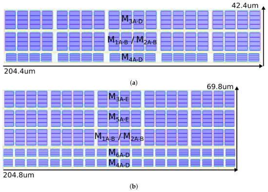
Figure 8.
Layout designs of the BD-OTAs. (a) Conventional BD-OTA layout. (b) Proposed BD-OTA layout.
4. Simulation Results
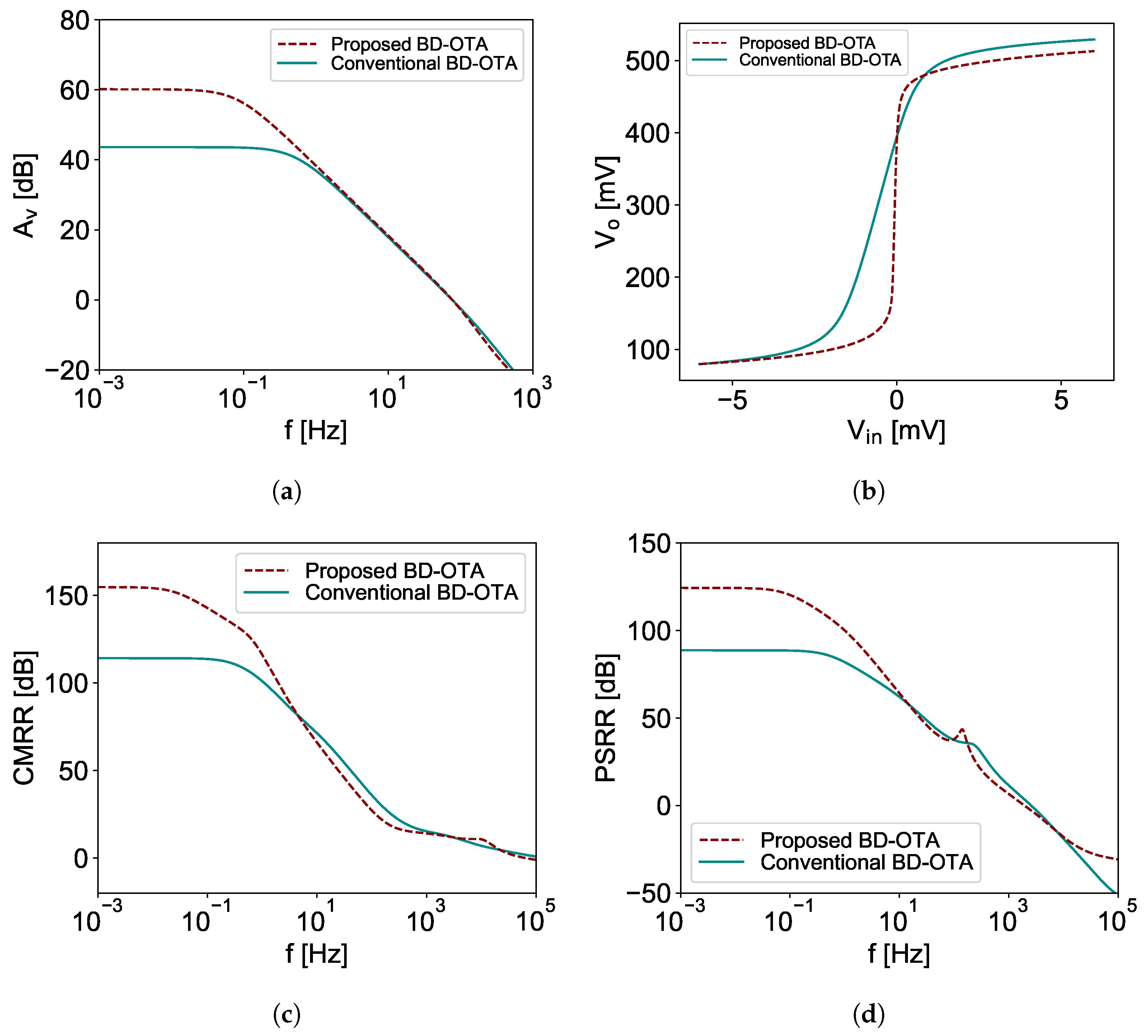
In this section, the post-layout simulation results referring to a TSMC 180 nm CMOS process for the conventional BD-OTA, and the proposed one, are reported. The circuits are considered to operate under the same conditions, i.e., 27 temperature, equal to 0.6 V, I equal to 100 pA, besides the typical process parameters. Characteristics from both OTAs were obtained by simulating the four testbenches shown in Figure 9. Figure 9a shows the integrator test bench used in the AC and DC simulations. This scheme allows the evaluation and comparison of DC open-loop gain, as also the gain-bandwidth product (GBW) of each OTA version. Then, Figure 10a shows the open-loop gain AC simulation results, and Figure 10b shows the DC simulation results.
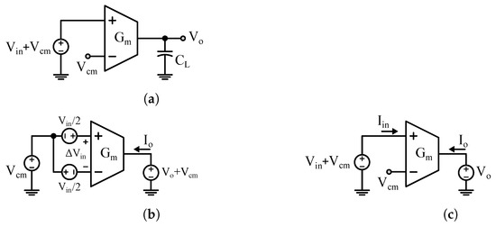
Figure 9.
OTA testbenches. (a) OTA-C integrator. (b) Transconductor (Symmetrical). (c) Transconductor (asymmetrical). (d) OTA-C low-pass filter. (e) Unity gain buffer.
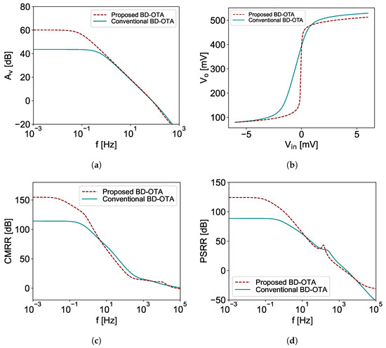
Figure 10.
Integrator test bench simulation results. (a) AC voltage gain transfer function. (b) DC voltage gain transfer function. (c) AC CMRR transfer function. (d) AC PSRR transfer function.
It can be noted that the use of improved mirrors increases DC gain without changing considerably the gain-bandwidth product of the OTA versions using the same differential pair, as they are biased with the same current. As expected, the proposed BD OTA with the enhanced mirror has lower transconductance, while keeping higher gain and the same linearity than the typical BD topology.
As the power supply rejection ratio (PSRR) is equal to the OTAs DC gain, there is a unity gain voltage between supply and output voltages. The common-mode rejection ratio (CMRR) is inherently increased by the use of improved mirrors, as the current source transistors also use improved self-biased cascode configuration. The CMRR and PSRR can be noted in Figure 10c,d, respectively. Table 3 summarizes the AC simulation results.
Table 3.
Integrator simulation results summary.
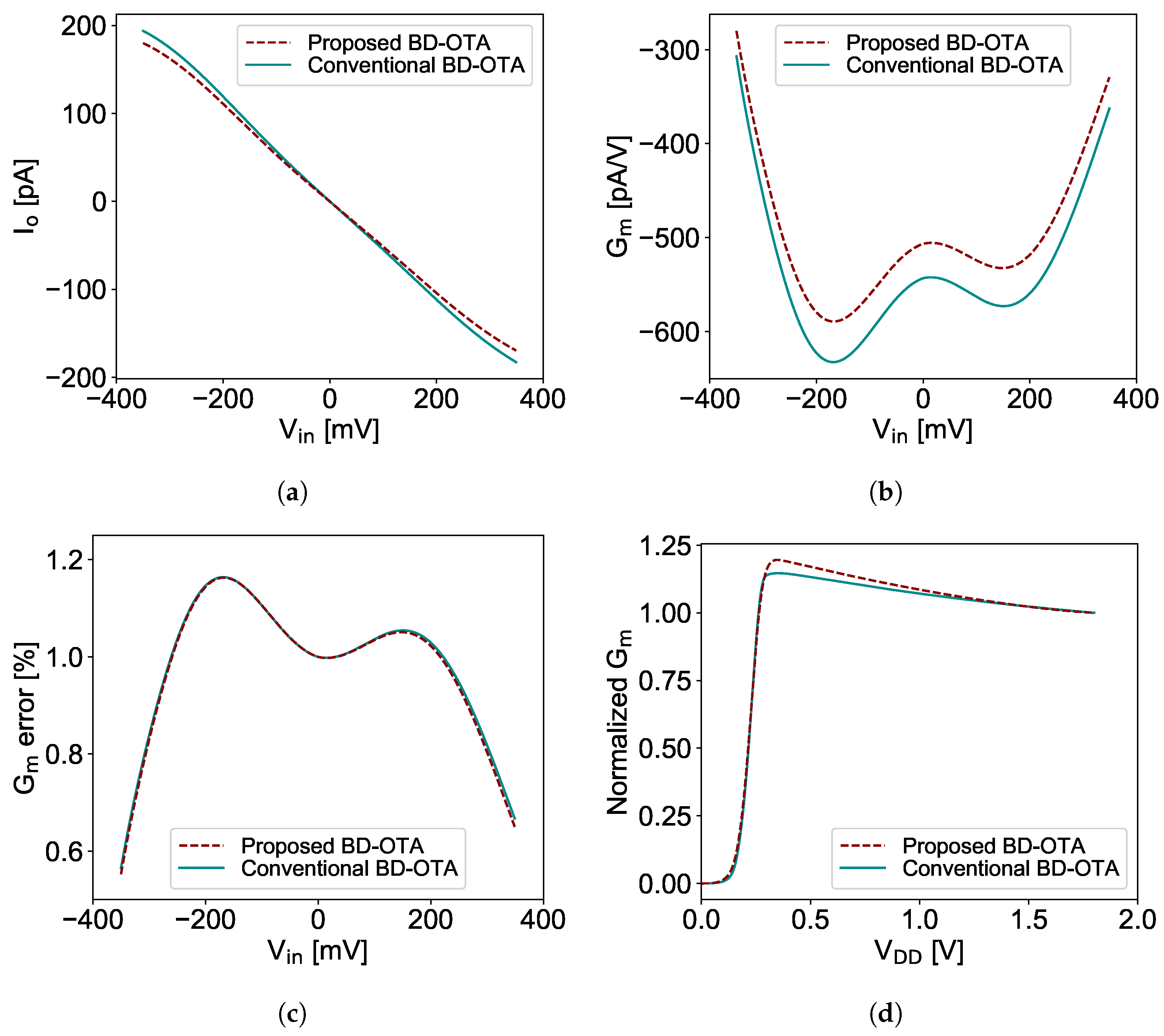
Figure 9c shows the testbench used in the DC simulations to compare the transconductance linearity of each OTA version. Figure 11a–c show, respectively, the output current, transconductance, and transconductance error for the conventional BD-OTA and for the proposed one.
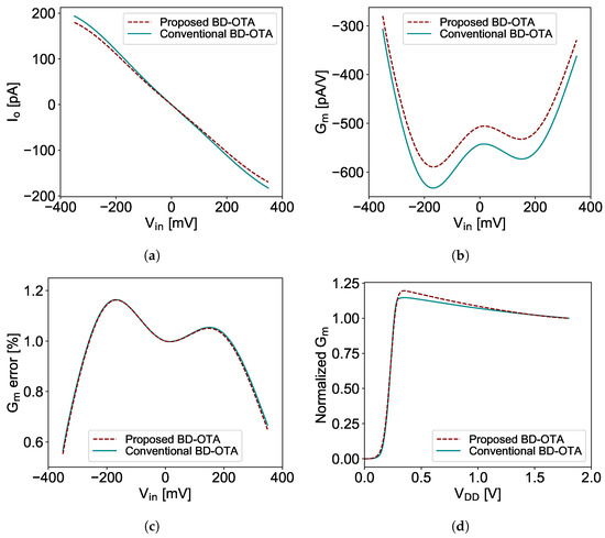
Figure 11.
Transconductor testbench simulation results. (a) Output current. (b) Tranconductance. (c) Transconductance error. (d) Normalized transconductance.
Table 4 summarizes the transconductance and impedance simulation results for I equal to 100 pA. Notice that BD OTAs have finite DC input impedances () as large as their output impedances (), which reduces considerably the effectiveness of the gain improving technique in practical use, where the OTAs are cascaded in OTA-C filters.
Table 4.
BD-OTAs DC results.
In Figure 11d, the transconductance normalized with respect to the supply voltage is shown. It is possible to note that both OTA versions work properly from a minimum of about 300 mV, which is feasible for implants and wearable biomedical trends. Unlike conventional gate-driven OTA topologies, which are limited by the minimum common-mode input voltage , and in which frequently are set to half to allow the current source transistors to operate in saturation, according to mentioned this limitation is mitigated in BD topologies. Besides the mentioned aspects, it is worth noticing that the minimum operational voltage, , is directly influenced by the current source, and the differential pair transistors channel inversion, hence which are themselves a function of the bias current, i.e., I. In this way, a higher biasing current would result in a larger linear input range and greater transconductance, on the other hand, also a higher minimum .
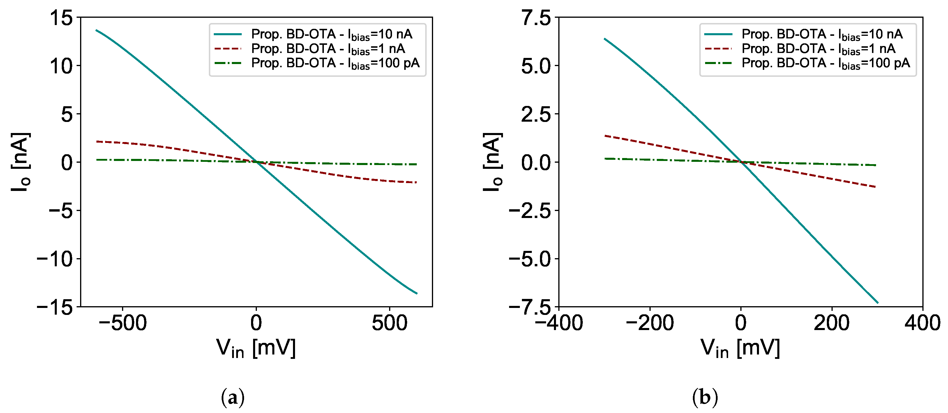
Figure 12a,b and Figure 13a,b show the nominal output current and its resulting transconductance for symmetrical and asymmetrical input voltage, according to the testbenches shown in Figure 9b,c, respectively. For the asymmetrical test, the inverting input is kept constant at , so mV, while, for the symmetrical input, both OTA inputs are at for = 0 V, and the differential input voltage excursion is doubled to mV. Moreover, for the asymmetrical testbench, the common mode input voltage varies with the input voltage , so . For the symmetrical testbench, is constant, as the average of the inverting and non-inverting input voltages are the same. It can be noticed, for both cases, that as the biasing current I increases, the transconductance increases almost proportionally.
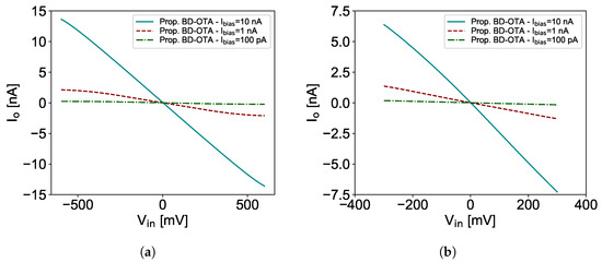
Figure 12.
Output current Io for (a) symmetrical, and (b) asymmetrical input voltage Vin, as a function of Ibias.
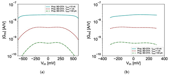
Figure 13.
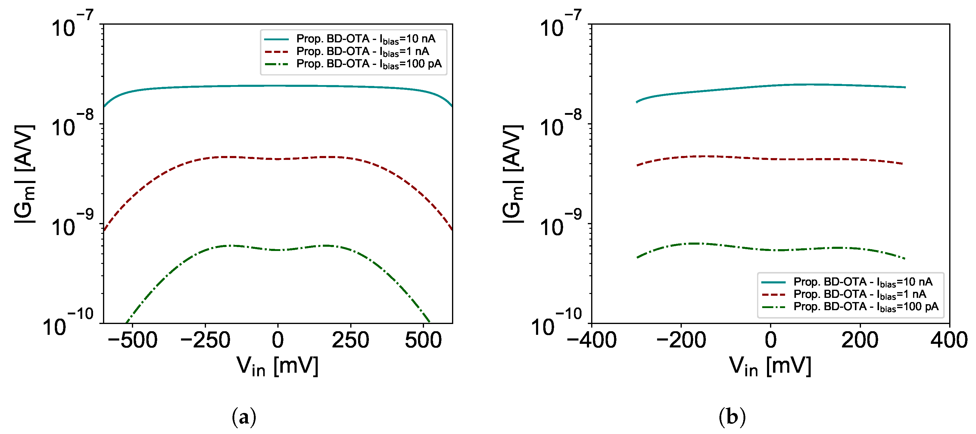
Nominal transconductance Gm for (a) symmetrical, and (b) asymmetrical input voltage Vin, as a function of Ibias.
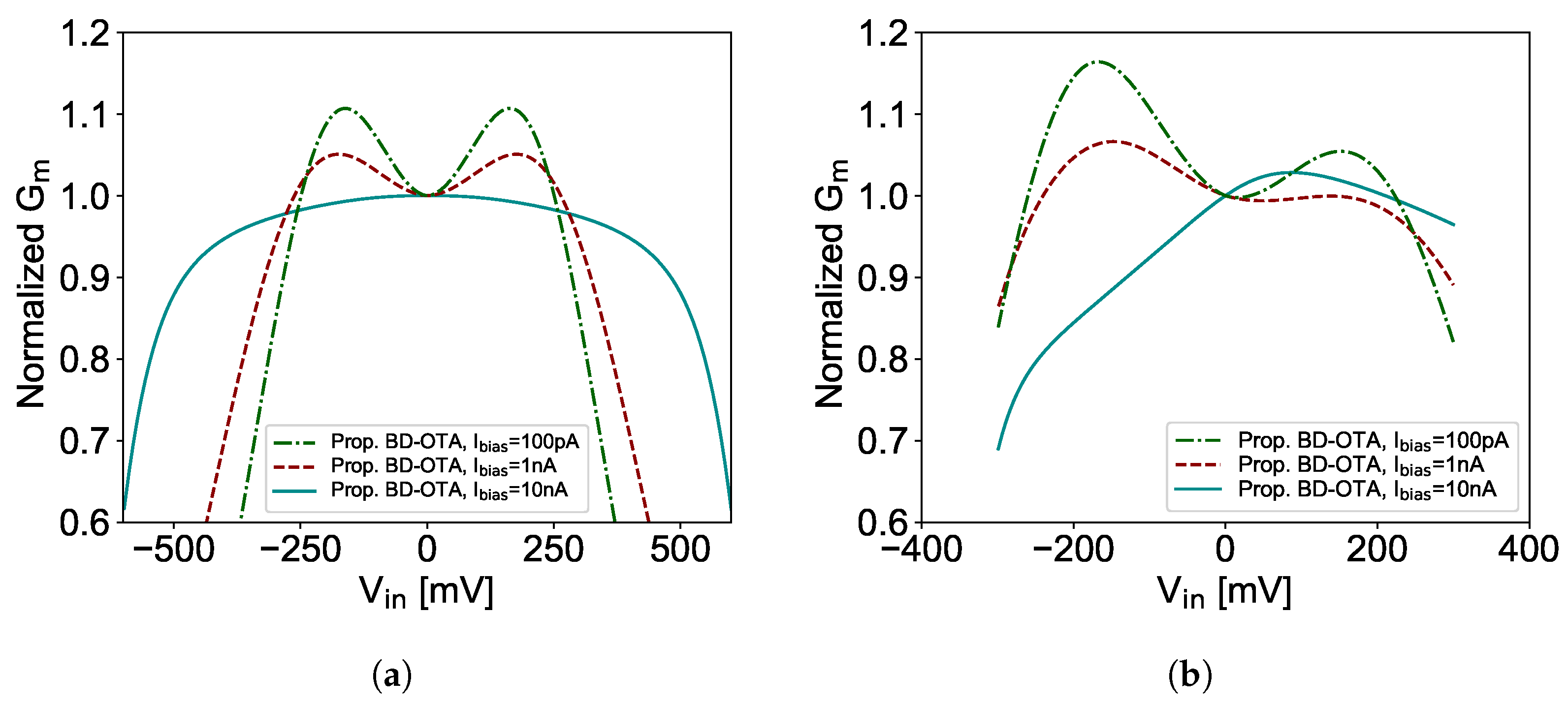
For a better comparison, for different biasing currents, the transconductances were normalized for , as shown in Figure 14a,b. It is clear for the asymmetrical input that the error is larger for . This happens for two reasons: the parasitic substrate current at the differential pair is extremely non-linear and the common-mode input voltage goes above the limit for I nA. For symmetrical input, the resulting is also symmetrical and the range is twice as high. It can also be noted that the shape of the curve changes as the current increases, which is expected, as the differential pair inversion increases.
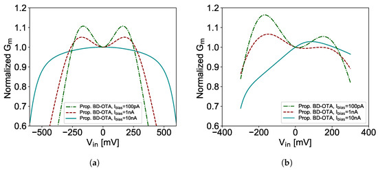
Figure 14.
Normalized transconductance Gm for (a) symmetrical, and (b) asymmetrical input voltage Vin, as a function of Ibias.
It is also important to notice that for single-ended OTA applications, normally, the input is not symmetrical. This is the case with most OTA-C filters, such as those based on integrators and active loads, as depicted in the testbenches shown in Figure 9a,d. For wider range and linearity, the single-ended OTA should be converted to its fully differential version, which needs extra biasing circuits for its output common-mode definition.
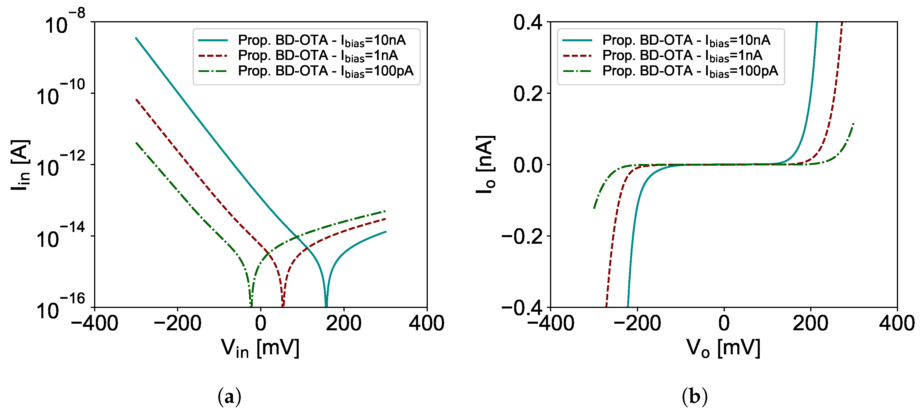
As previously explained, the parasitic input current is one of the causes of transconductance asymmetry. This parasitic current is shown in Figure 15a, and is a function of the input voltage and biasing current. There is a single point where the input current is zero, which happens when the differential pair PMOS transistor bulk-terminal voltage is equal to its source-terminal voltage. For input voltages below this point, the transistor is forward-body-biased and the parasitic current grows exponentially. For voltages above this point, the parasitic current is almost constant, consequently, the input conductance is very small. Figure 15b shows the OTA output current for both inputs at and the output sweeping from 0 to 600 mV. As can be seen, the output current, even considering that the current mirrors attenuate the differential pair output current, is considerably larger than the parasitic current for a large range.
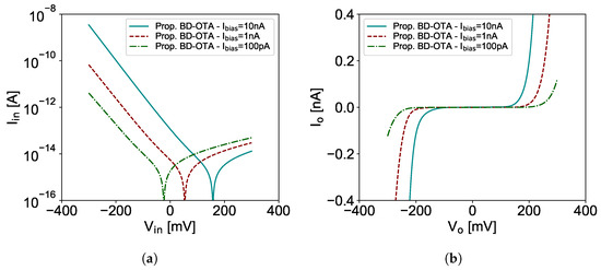
Figure 15.
Nominal (a) input current Iin × input voltage Vin, and (b) output current Io × output voltage Vo, as a function of Ibias.
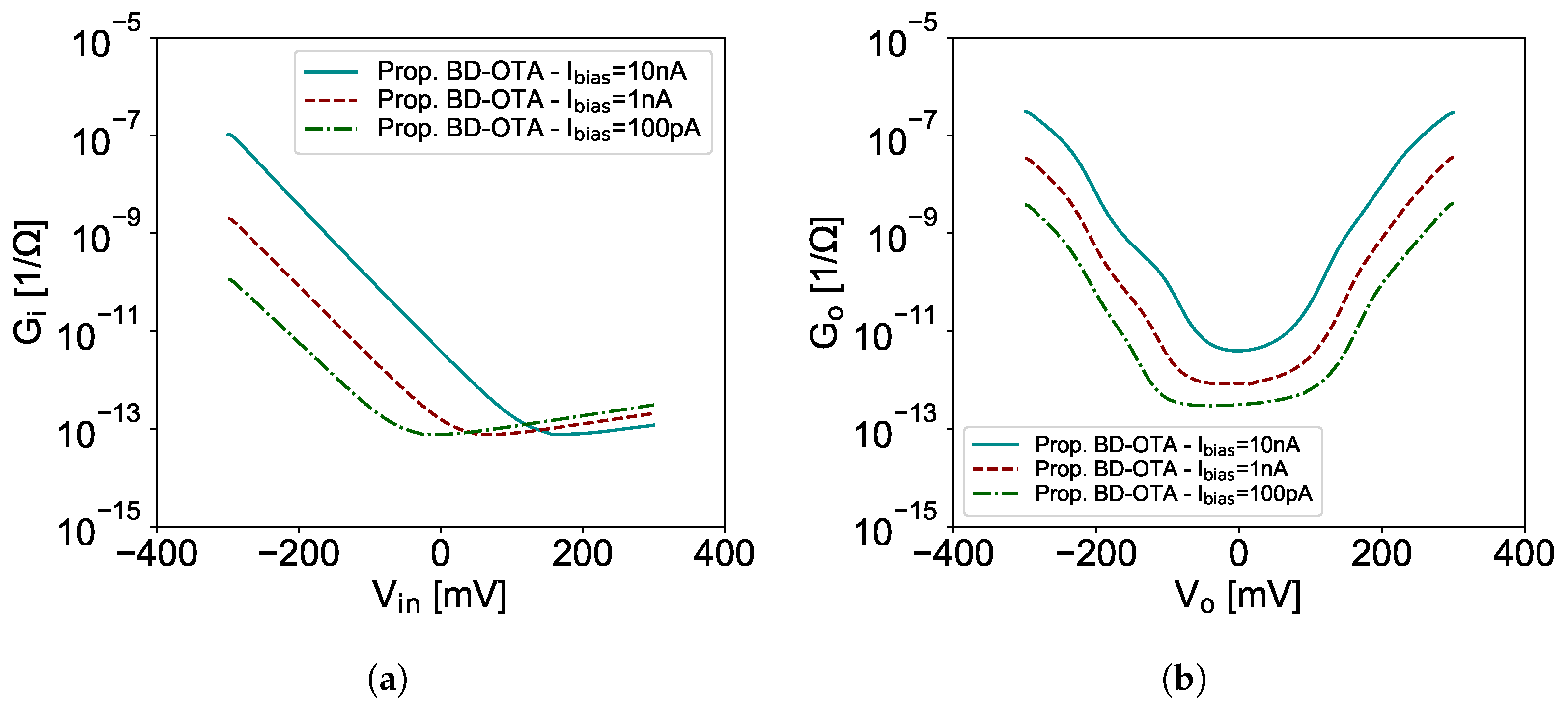
The input and output conductances can be derived from the input and output currents, as shown in Figure 16a,b, respectively. It is worth noting that for OTA-C filter applications, the OTA outputs terminals will be connected to other OTAs input terminals. The main advantage of the proposed improved self-cascode current mirror is to decrease the output conductance as it increases the output resistance. If the input conductance of the subsequent stage is greater than the output conductance, the technique effectiveness is reduced.
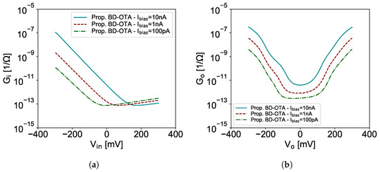
Figure 16.
Normalized (a) input conductance Gi, and (b) output conductance Go as a function of Ibias.
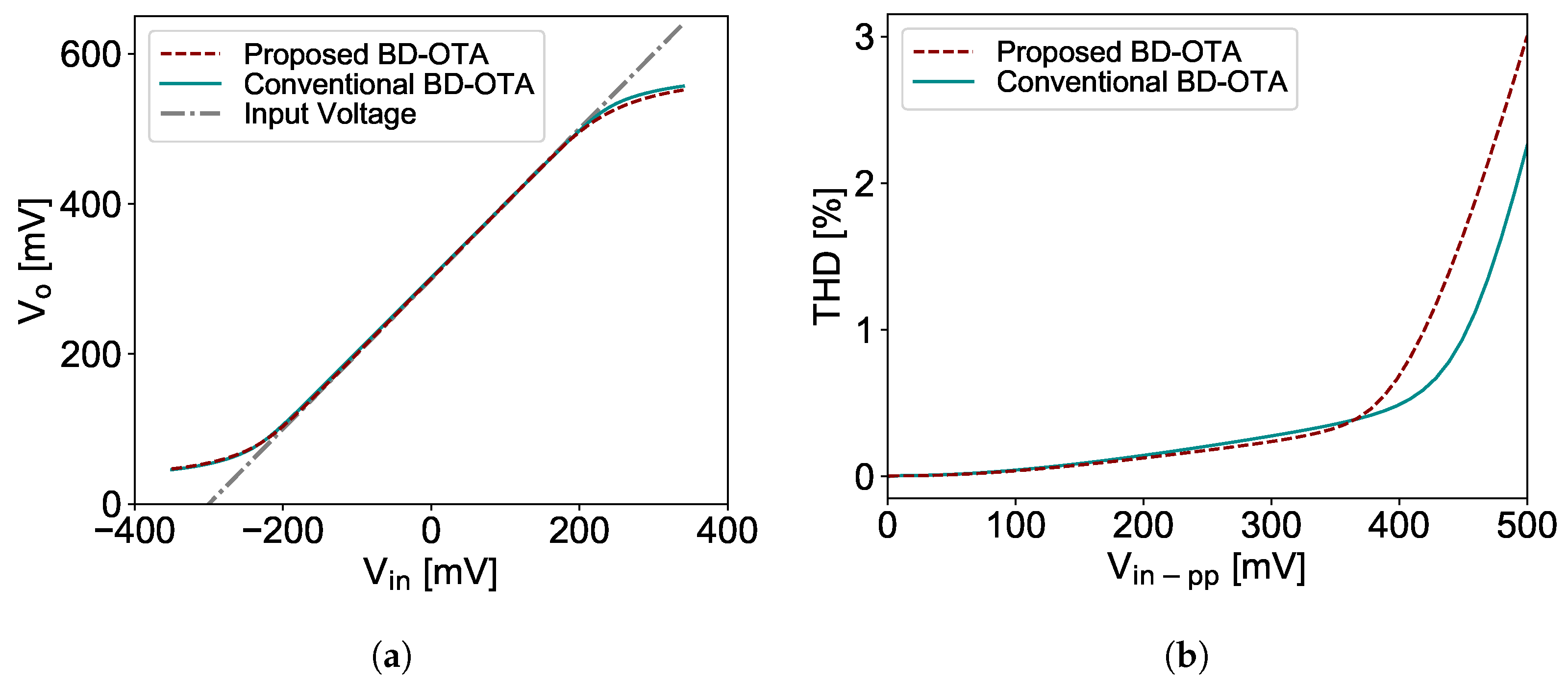
In order to compare the linearity OTAs, the unity gain low-pass OTA-C filter testbench shown in Figure 9d was used in DC and transient simulations. Figure 17a,b show, respectively, the DC transfer functions, transient, and the total harmonic distortion (THD) for both OTAs. It is possible to observe that the BD OTAs have almost the same full input range. Figure 17b shows the total harmonic distortion versus input plotted as a function of input signal amplitude. For both OTAs, one can observe that THD is lower for smaller signal amplitudes. They exhibit approximately the same amount of distortion of 0.07% as a result of a 300 mV amplitude input signal at 100 mHz. As the input voltage amplitude increases, the proposed OTA reaches ≈ 1% THD (−39.8 dB), SNR equal to 56.6 dB for a = 405 mV at 100 mHz signal.
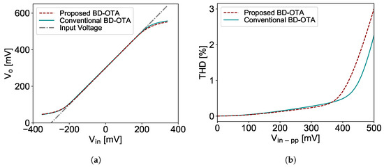
Figure 17.
Low-pass testbench simulation results. (a) Transfer functions. (b) Total harmonic distortion.
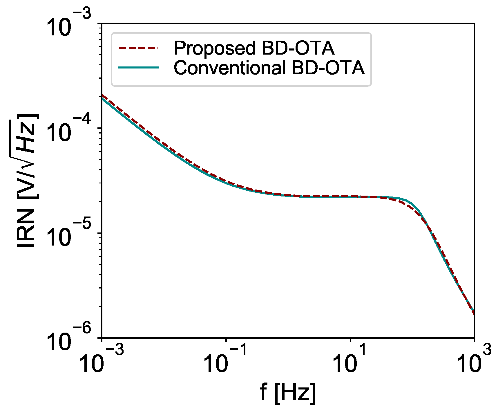
Figure 18 shows the input-referred noise (IRN) for both OTA versions configured as a unit-gain buffer. Since both OTA versions have the same transistor dimensions, differing only by the adopted current mirror topology, there is a slight difference in IRN of conventional BD-OTA and the proposed one. The IRN in the proposed topology is equal to 246 μV, and 237 μV in the other, both obtained by integrating noise from 10 mHz–1 kHz.
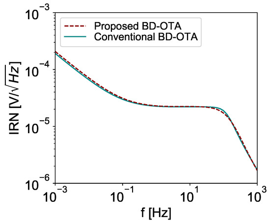
Figure 18.
Unity gain buffer testbench simulation results—input-referred noise.
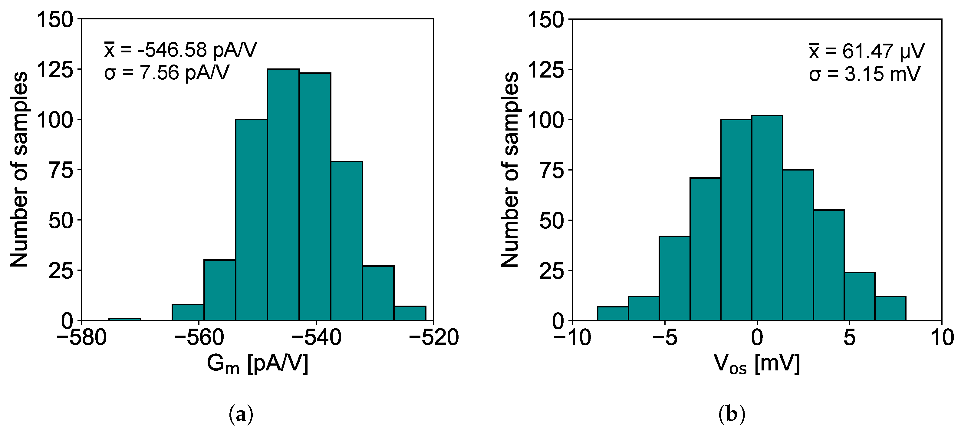
By using the transconductor (Figure 9c) and low-pass filter (Figure 9d) testbenches, 500 runs of Monte Carlo have been carried out for evaluation of transconductance and offset voltage, respectively. Figure 19a,b show the results for the Monte Carlo process and mismatch analysis of the proposed BD-OTA. These results are summarized in Table 5. On this basis, it is possible to conclude that the proposed BD-OTA besides a lower transconductance feature, has a considerably less input voltage offset than the conventional BD-OTA.
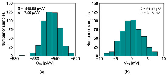
Figure 19.
Five hundred runs of Monte Carlo simulations analyzing process and mismatch with the proposed BD-OTA. (a) Transconductance. (b) Offset.
Table 5.
Monte Carlo simulation results.
Table 6 compares the performance of the proposed OTA with the state-of-art low-transconductance OTAs. The previous work proposed by us [48] presented a 450 pA/V OTA with small power consumption but lower gain, CMRR, and PSRR, despite being based on non-unitary current gain through the splitting current technique, it achieved a poorer performance with respect to the present work. In [49], a low-transconductance amplifier has been proposed based on the channel-length-modulation effect (Early effect). This solution shows a high IRN. Such an IRN is 3x smaller in the proposed topology while keeping lower transconductance, power consumption, and higher CMRR as also PSRR features. The OTA proposed by [28] is similar to the conventional OTA presented in this work. The difference is in the rectangular arrays used to increase the gain and in no linearization technique employed. Another low- topology presented by [50] uses a linearization technique that relies on a combination of source degeneration with an active attenuator. Despite the valuable linearity and gain achieved, the power consumption, and transconductance may not be suitable to the constraints of biomedical implants or bio-sensing operations. The architecture proposed by [51] is another channel length modulated OTA which contains the same V-I conversion scheme as presented in [49] but requires a higher supply voltage.
Table 6.
Comparison of Low-G OTA topologies.
5. Conclusions
The paper presented a bulk-driven symmetrical OTA based on a self-cascode current mirror with source degeneration to provide a high-gain, high linearity, and low- topology. The proposed low- topology shown a valuable performance that is suitable for new biomedical IC applications. In particular, the new topology achieved the lowest power consumption compared with the state-of-art topologies, in addition to high gain, linearity, low transconductance, and IRN. Moreover, the circuit obtained the highest CMRR and high PSRR, which turns the proposed OTA into an interesting topology as a basic block for OTA-C filters.
Author Contributions
Conceptualization, R.S.S. and L.H.R.; methodology, R.S.S. and L.H.R.; validation, R.S.S. and L.H.R.; formal analysis, R.S.S. and L.H.R.; investigation, R.S.S. and L.H.R.; resources, C.R.R.; data curation, L.H.R.; writing—original draft preparation, L.H.R.; writing—review and editing, O.A. and C.R.R.; visualization, L.H.R.; supervision, O.A. and C.R.R.; project administration, C.R.R.; funding acquisition, C.R.R. All authors have read and agreed to the published version of the manuscript.
Funding
Brazilian National Council for Scientific and Technological Development (CNPq), and to the Coordination of Improvement of Higher Education Personnel—Brazil (CAPES)—Finance Code 001 for partial financial support. This work also has been partially supported in Brazil by PrInt CAPES-UFSC “Automation 4.0”.
Data Availability Statement
Data are contained within the article.
Acknowledgments
The authors are grateful to the Brazilian National Council for Scientific and Technological Development (CNPq), the Coordination of Improvement of Higher Education Personnel—Brazil (CAPES), and CAPES-UFSC PrInt for the financial support.
Conflicts of Interest
The authors declare no conflict of interest.
Abbreviations
The following abbreviations are used in this manuscript:
| ACM | Advanced Compact Model |
| BD | Bulk-driven |
| CMOS | Complementary Metal-Oxide Semiconductor |
| CM | Current Mirror |
| CMR | Common-Mode Range |
| CMRR | Common-Mode Rejection Ratio |
| GBW | Gain–Bandwidth Product |
| OTA | Operational Transconductance Amplifier |
| SCCM | Self-Cascode Current Mirror |
| IRF | Equivalent Input Referred Noise |
| ISCCM | Improved Self-Cascode Current Mirror |
| PSRR | Power Supply Rejection Ratio |
| SNR | Signal-to-Noise Ratio |
| THD | Total Harmonic Distortion |
References
- Khateb, F.; Kulej, T.; Akbari, M.; Kumngern, M. 0.5-V High linear and wide tunable OTA for biomedical applications. IEEE Access 2021, 9, 103784–103794. [Google Scholar] [CrossRef]
- Sanchotene Silva, R.; Pereira Luiz, L.; Cherem Schneider, M.; Galup-Montoro, C. A Test Chip for Characterization of the Series Association of MOSFETs. IEEE Trans. Very Large Scale Integr. (VLSI) Syst. 2019, 27, 1967–1971. [Google Scholar] [CrossRef]
- Bano, S.; Narejo, G.; Shan, S. Power Efficient Fully Differential Bulk Driven OTA for Portable Biomedical Application. Electronics 2018, 7, 41. [Google Scholar] [CrossRef] [Green Version]
- Ballo, A.; Pennisi, S.; Scotti, G. 0.5 V CMOS Inverter-Based Transconductance Amplifier with Quiescent Current Control. J. Low Power Electron. Appl. 2021, 11, 37. [Google Scholar] [CrossRef]
- Giustolisi, G.; Palumbo, G. A gm/ID-Based Design Strategy for IoT and Ultra-Low-Power OTAs with Fast-Settling and Large Capacitive Loads. J. Low Power Electron. Appl. 2021, 11, 21. [Google Scholar] [CrossRef]
- Centurelli, F.; Della Sala, R.; Monsurrò, P.; Scotti, G.; Trifiletti, A. A 0.3 V Rail-to-Rail Ultra-Low-Power OTA with Improved Bandwidth and Slew Rate. J. Low Power Electron. Appl. 2021, 11, 19. [Google Scholar] [CrossRef]
- Centurelli, F.; Della Sala, R.; Monsurrò, P.; Scotti, G.; Trifiletti, A. A Novel OTA Architecture Exploiting Current Gain Stages to Boost Bandwidth and Slew-Rate. Electronics 2021, 10, 1638. [Google Scholar] [CrossRef]
- Centurelli, F.; Della Sala, R.; Scotti, G.; Trifiletti, A. A 0.3 V, Rail-to-Rail, Ultralow-Power, Non-Tailed, Body-Driven, Sub-Threshold Amplifier. Appl. Sci. 2021, 11, 2528. [Google Scholar] [CrossRef]
- Jayasimha, T.; Vijayalakshmi, A. Low Pass Filter Using ECG Detection for OTA-C. Ir. Interdiscip. J. Sci. Res. 2018, 2, 94–100. [Google Scholar]
- Yehoshuva, C.; Rakhi, R.; Anto, D.; Kaurati, S. 0.5 V, Ultra Low Power Multi Standard Gm-C Filter for Biomedical Applications. In Proceedings of the 2016 IEEE International Conference on Recent Trends in Electronics, Information and Communication Technology (RTEICT), Bangalore, India, 20–21 May 2016. [Google Scholar]
- Kulej, T.; Khateb, F. A Compact 0.3-V Class AB Bulk-Driven OTA. IEEE Trans. Very Large Scale Integr. (VLSI) Syst. 2020, 28, 224–232. [Google Scholar] [CrossRef]
- Kulej, T.; Khateb, F. A 0.3-V 98-dB Rail-to-Rail OTA in 0.18 μm CMOS. IEEE Access 2020, 8, 27459–27467. [Google Scholar] [CrossRef]
- Rodovalho, L.H.; Aiello, O.; Rodrigues, C.R. Ultra-low-voltage inverter-based operational transconductance amplifiers with voltage gain enhancement by improved composite transistors. Electronics 2020, 9, 1410. [Google Scholar] [CrossRef]
- Rodovalho, L.H.; Ramos Rodrigues, C.; Aiello, O. Self-Biased and Supply-Voltage Scalable Inverter-Based Operational Transconductance Amplifier with Improved Composite Transistors. Electronics 2021, 10, 935. [Google Scholar] [CrossRef]
- Toledo, P.; Crovetti, P.; Aiello, O.; Alioto, M. Fully Digital Rail-to-Rail OTA With Sub-1000-μm² Area, 250-mV Minimum Supply, and nW Power at 150-pF Load in 180 nm. IEEE Solid-State Circuits Lett. 2020, 3, 474–477. [Google Scholar] [CrossRef]
- Fassio, L.; Lin, L.; De Rose, R.; Lanuzza, M.; Crupi, F.; Alioto, M. Trimming-Less Voltage Reference for Highly Uncertain Harvesting Down to 0.25 V, 5.4 pW. IEEE J.-Solid-State Circuits 2021, 3134–3144. [Google Scholar] [CrossRef]
- Aiello, O. Design of an Ultra-Low Voltage Bias Current Generator Highly Immune to Electromagnetic Interference. J. Low Power Electron. Appl. 2021, 11, 6. [Google Scholar] [CrossRef]
- Aiello, O.; Crovetti, P.; Alioto, M. A Sub-Leakage PW-Power HZ-Range Relaxation Oscillator Operating with 0.3 V–1.8 V Unregulated Supply. In Proceedings of the 2018 IEEE Symposium on VLSI Circuits, Honolulu, HI, USA, 18–22 June 2018; pp. 119–120. [Google Scholar] [CrossRef]
- Lee, S.Y.; Cheng, C.J. Systematic Design and Modeling of a OTA-C Filter for Portable ECG Detection. IEEE Trans. Biomed. Circuits Syst. 2009, 3, 53–64. [Google Scholar] [CrossRef]
- Veeravalli, A.; Sánchez-Sinencio, E.; Silva-Martínez, J. Transconductance amplifier structures with very small transconductances: A comparative design approach. IEEE J.-Solid-State Circuits 2002, 37, 770–775. [Google Scholar] [CrossRef] [Green Version]
- Kinget, P.; Steyaert, M.; Van der Spiegel, J. Full analog CMOS integration of very large time constants for synaptic transfer in neural networks. Analog Integr. Circuits Signal Process. 1992, 2, 281–295. [Google Scholar] [CrossRef]
- Fiorelli, R.; Arnaud, A.; Galup-Montoro, C. Series-parallel association of transistors for the reduction of random offset in non-unity gain current mirrors. In Proceedings of the 2004 IEEE International Symposium on Circuits and Systems (IEEE Cat. No. 04CH37512), Vancouver, BC, Canada, 23–26 May 2004; Volume 1, pp. 1–881. [Google Scholar]
- Arnaud, A.; Fiorelli, R.; Galup-Montoro, C. Nanowatt, sub-nS OTAs, with sub-10-mV input offset, using series-parallel current mirrors. IEEE J.-Solid-State Circuits 2006, 41, 2009–2018. [Google Scholar] [CrossRef]
- Blalock, B.J.; Allen, P.E.; Rincon-Mora, G.A. Designing 1-V op amps using standard digital CMOS technology. IEEE Trans. Circuits Syst. II Analog Digit. Signal Process. 1998, 45, 769–780. [Google Scholar] [CrossRef] [Green Version]
- Chatterjee, S.; Tsividis, Y.; Kinget, P. 0.5-V analog circuit techniques and their application in OTA and filter design. IEEE J.-Solid-State Circuits 2005, 40, 2373–2387. [Google Scholar] [CrossRef]
- Carrillo, J.M.; Torelli, G.; Valverde, R.P.A.; Duque-Carrillo, J.F. 1-V rail-to-rail CMOS opamp with improved bulk-driven input stage. IEEE J.-Solid-State Circuits 2007, 42, 508–517. [Google Scholar] [CrossRef]
- Cotrim, E.D.C.; de Carvalho Ferreira, L.H. An ultra-low-power CMOS symmetrical OTA for low-frequency Gm-C applications. Analog Integr. Circuits Signal Process. 2012, 71, 275–282. [Google Scholar] [CrossRef]
- Colletta, G.D.; Ferreira, L.H.; Pimenta, T.C. A 0.25-V 22-nS symmetrical bulk-driven OTA for low-frequency Gm-C applications in 130-nm digital CMOS process. Analog Integr. Circuits Signal Process. 2014, 81, 377–383. [Google Scholar] [CrossRef]
- Sharan, T.; Bhadauria, V. Sub-threshold, cascode compensated, bulk-driven OTAs with enhanced gain and phase-margin. Microelectron. J. 2016, 54, 150–165. [Google Scholar] [CrossRef]
- del Risco Sánchez, A.; Moreno, R.L.; Ferreira, L.H.; Crepaldi, P.C. Biasing technique to improve total harmonic distortion in an ultra-low-power operational transconductance amplifier. IET Circuits Devices Syst. 2019, 13, 920–927. [Google Scholar] [CrossRef]
- Galup-Montoro, C.; Schneider, M.C.; Loss, I.J. Series-parallel association of FET’s for high gain and high frequency applications. IEEE J.-Solid-State Circuits 1994, 29, 1094–1101. [Google Scholar] [CrossRef]
- Comer, D.T.; Comer, D.J.; Li, L. A high-gain complementary metal-oxide semiconductor op amp using composite cascode stages. Int. J. Electron. 2010, 97, 637–646. [Google Scholar] [CrossRef]
- Akbari, M.; Hashemipour, O. A 0.6-V, 0.4-μW bulk-driven operational amplifier with rail-to-rail input/output swing. Analog Integr. Circuits Signal Process. 2016, 86, 341–351. [Google Scholar] [CrossRef]
- Sharan, T.; Chetri, P.; Bhadauria, V. Ultra-low-power bulk-driven fully differential subthreshold OTAs with partial positive feedback for Gm-C filters. Analog Integr. Circuits Signal Process. 2018, 94, 427–447. [Google Scholar] [CrossRef]
- Baek, K.J.; Gim, J.M.; Kim, H.S.; Na, K.Y.; Kim, N.S.; Kim, Y.S. Analogue circuit design methodology using self-cascode structures. Electron. Lett. 2013, 49, 591–592. [Google Scholar] [CrossRef]
- Xu, D.; Liu, L.; Xu, S. High DC gain self-cascode structure of OTA design with bandwidth enhancement. Electron. Lett. 2016, 52, 740–742. [Google Scholar] [CrossRef]
- Niranjan, V.; Kumar, A.; Jain, S.B. Composite transistor cell using dynamic body bias for high gain and low-voltage applications. J. Circuits Syst. Comput. 2014, 23, 1450108. [Google Scholar] [CrossRef]
- Krummenacher, F.; Joehl, N. A 4-MHz CMOS continuous-time filter with on-chip automatic tuning. IEEE J.-Solid-State Circuits 1988, 23, 750–758. [Google Scholar] [CrossRef]
- Braga, R.A.; Ferreira, L.H.; Coletta, G.D.; Dutra, O.O. A 0.25-V calibration-less inverter-based OTA for low-frequency Gm-C applications. Microelectron. J. 2019, 83, 62–72. [Google Scholar] [CrossRef]
- Schneider, M.C.; Galup-Montoro, C. CMOS Analog Design Using All-Region MOSFET Modeling; Cambridge University Press: Cambridge UK, 2010. [Google Scholar]
- Wilson, G.R. A monolithic junction FET-NPN operational amplifier. IEEE J.-Solid-State Circuits 1968, 3, 341–348. [Google Scholar] [CrossRef]
- De Ceuster, D.; Flandre, D.; Colinge, J.P.; Cristoloveanu, S. Improvement of SOI MOS current-mirror performances using serial-parallel association of transistors. Electron. Lett. 1996, 32, 278–279. [Google Scholar] [CrossRef]
- Rodovalho, L.H. Push–pull based operational transconductor amplifier topologies for ultra low voltage supplies. Analog Integr. Circuits Signal Process. 2020, 1–14. [Google Scholar] [CrossRef]
- Haga, Y.; Zare-Hoseini, H.; Berkovi, L.; Kale, I. Design of a 0.8 Volt fully differential CMOS OTA using the bulk-driven technique. In Proceedings of the 2005 IEEE International Symposium on Circuits and Systems, Kobe, Japan, 23–26 May 2005; pp. 220–223. [Google Scholar]
- Ferreira, L.H.; Sonkusale, S.R. A 60-dB gain OTA operating at 0.25-V power supply in 130-nm digital CMOS process. IEEE Trans. Circuits Syst. Regul. Pap. 2014, 61, 1609–1617. [Google Scholar] [CrossRef]
- Kuo, K.C.; Leuciuc, A. A linear MOS transconductor using source degeneration and adaptive biasing. IEEE Trans. Circuits Syst. II Analog Digit. Signal Process. 2001, 48, 937–943. [Google Scholar]
- Galup-Montoro, C.; Schneider, M.C.; Cunha, A.I.A.; de Sousa, F.R.; Klimach, H.; Siebel, O.F. The Advanced Compact MOSFET (ACM) Model for Circuit Analysis and Design. In Proceedings of the 2007 IEEE Custom Integrated Circuits Conference, San Jose, CA, USA, 16–19 September 2007; pp. 519–526. [Google Scholar] [CrossRef]
- Rodovalho, L.H.; Silva, R.S.; Rodrigues, C.R. A 1V, 450pS OTA Based on Current-Splitting and Modified Series-Parallel Mirrors. In Proceedings of the 2021 IEEE 12th Latin America Symposium on Circuits and System (LASCAS), Arequipa, Peru, 21–24 February 2021; pp. 1–4. [Google Scholar] [CrossRef]
- Jakusz, J.; Jendernalik, W.; Blakiewicz, G.; Kłosowski, M.; Szczepański, S. A 1-nS 1-V Sub-1-µW Linear CMOS OTA with Rail-to-Rail Input for Hz-Band Sensory Interfaces. Sensors 2020, 20, 3303. [Google Scholar] [CrossRef]
- Soares, C.F.; de Moraes, G.S.; Petraglia, A. A low-transconductance OTA with improved linearity suitable for low-frequency Gm-C filters. Microelectron. J. 2014, 45, 1499–1507. [Google Scholar] [CrossRef]
- Huang, Y.; Drakakis, E.M.; Toumazou, C. A 30pA/V–25μA/V linear CMOS channel-length-modulation OTA. Microelectron. J. 2009, 40, 1458–1465. [Google Scholar] [CrossRef]


Publisher’s Note: MDPI stays neutral with regard to jurisdictional claims in published maps and institutional affiliations. |
© 2021 by the authors. Licensee MDPI, Basel, Switzerland. This article is an open access article distributed under the terms and conditions of the Creative Commons Attribution (CC BY) license (https://creativecommons.org/licenses/by/4.0/).