Abstract
Large-area and uniform plasmonic nanostructures have often been fabricated by simply evaporating noble metals such as gold and silver on a variety of nanotemplates such as nanopores, nanotubes, and nanorods. However, some highly uniform nanotemplates are limited to be utilized by long, complex, and expensive fabrication. Here, we introduce a cost-effective and high-throughput fabrication method for plasmonic interference coupled nanostructures based on quasi-uniform anodic aluminum oxide (QU-AAO) nanotemplates. Industrial aluminum, with a purity of 99.5%, and copper were used as a base template and a plasmonic material, respectively. The combination of these modifications saves more than 18 h of fabrication time and reduces the cost of fabrication 30-fold. From optical reflectance data, we found that QU-AAO based plasmonic nanostructures exhibit similar optical behaviors to highly ordered (HO) AAO-based nanostructures. By adjusting the thickness of the AAO layer and its pore size, we could easily control the optical properties of the nanostructures. Thus, we expect that QU-AAO might be effectively utilized for commercial plasmonic applications.
1. Introduction
Plasmonic nanostructures are critically promising for next-generation optical devices such as displays and optical sensors [1,2,3,4,5,6,7,8]. Particularly, large-area plasmonic nanostructures are quite important to design and develop industrial plasmonic applications [9,10,11,12,13]. Normally, previous fabrication techniques for large-area plasmonic structures are limited by being high in cost, with low throughput and low reproducibility [14,15,16]. To overcome these disadvantages, template-based lithography for large-area uniform plasmonic nanostructures has been developed, but the large-area uniform template fabrications still are high in cost and their throughputs are very low [17,18,19,20].
Anodic aluminum oxide (AAO) films containing self-ordered nanoscale pores have been extensively studied, as they can be served as a versatile template in various applications, including nanostructure synthesis, catalysis, and in biosensors [21,22,23,24,25,26,27,28,29,30,31]. For instance, controlled electrochemical treatments could produce highly reproducible nanotemplates with various pore sizes and array patterns [23,24,25]. A large surface area ratio over volume in AAO results in enhanced chemical reaction in catalytic applications [26,27]. The periodic nanoarrays are also excellent platforms for biosensing applications [28,29]. Noble metals such as gold and silver, deposited on AAO nanopores, for instance, form hotspots in surface-enhanced Raman spectroscopy (SERS) measurement. With an improved AAO fabrication, high SERS sensitivity (i.e., a detection limit of ~fM) has been recently demonstrated [30,31,32,33,34].
Many previous studies have used highly ordered AAO (HO-AAO), which often raises issues such as a long fabrication time, high cost, and a low throughput [35,36,37]. HO-AAO nanotemplates are normally obtained by the standard two-step anodization process, where two subsequent anodizations with chemical etching in between produce a closely-packed and self-ordered honeycomb array of alumina nanoholes [23,24]. The process includes a long anodization period (i.e., more than 12 h in the first step) and a wet etching (i.e., more than 6 h) procedure. Furthermore, HO-AAO structures require expensive high purity (e.g., 99.999%) aluminum (Al) substrates, and a notable amount of Al is consumed during the etching process. Previously, our group also utilized HO-AAO as large-area uniform plasmonic templates, where we have investigated plasmonic interference coupling effects [38,39,40]. When the constructive interference was matched with the plasmonic layer, it mediated strong plasmonic absorption. We could easily control the strong plasmonic absorption by tailoring the thickness and pore size of the HO-AAO layer. Particularly, we could develop uniform plasmonic core-satellite structures by controlling the morphology of the HO-AAO. However, for the practical usage of AAO in various industrial applications, a low-cost and high-throughput fabrication method needs to be investigated.
In this study, we present a cost-effective and high-throughput fabrication method for plasmonic interference coupled nanostructures for use in various plasmonic applications. While achieving similar optical properties as the traditional method based on HO-AAO templates, we are able to significantly reduce the total fabrication time and cost. This is realized by several modifications of the fabrication procedures. First, we start the process with a relatively inexpensive Al substrate (i.e., a purity of 99.5%) which costs 30 times less than the high purity Al substrate of 99.999%. Second, we reduce the two-step anodization process to a single step, which saves more than 18 h of fabrication time, thus producing quasi-uniform (QU) AAO templates. Third, we use copper as the plasmonic material, observing similar optical responses as when gold and silver are used. This suggests even further cost savings by using copper instead of expensive noble metals. The optical properties are characterized by reflectance measurements in the visible wavelength range. By controlling the AAO thickness and its pore size, we are able to tune the resonance wavelength in the reflectance spectrum and realize a similar optical response when compared to the traditionally fabricated HO-AAO-based plasmonic nanostructures. We also find that inexpensive coating materials such as copper can be as good as noble metals. Furthermore, we demonstrate that such a low-cost plasmonic interference coupled nanostructure could be achieved on a flexible platform (i.e., a flexible optical nanodevice). As a demonstration of the plasmonic characteristics, we perform SERS measurements with Rhodamine 6G (R6G) dye molecules on our QU-AAO-based plasmonic nanostructures. The method developed in this paper yields a cost-effective, high-throughput and large-area fabrication of AAO plasmonic nanostructures suitable for various commercial plasmonic applications.
2. Materials and Methods
2.1. Fabrication of AAO Nanostructures
Aluminum (Al) sheets with the purity of 99.999% (Sigma-Aldrich, Saint Louis, MO, USA) and 99.5% (Sigma-Aldrich) were prepared to compare the morphological and optical properties of the nanostructures. To remove the existing oxide layer and smoothen the rough surface, an electropolishing process was applied to the pristine Al substrate prior to any anodization process. This process was done by immersing the substrate into a mixture of perchloric acid (SAMCHUN, Seoul, Korea) and ethanol (HClO4:C2H5OH = 1:4 volumetric ratio) and connecting it to the positive terminal of a 20 V DC power supply (i.e., an anode) at a temperature of 7 °C while a platinum plate was connected to the cathode terminal. The distance between electrodes was about 2 cm. When DC voltage was applied, the metal surface was dissolved into the electrolyte while a current flowed from the anode to the cathode. After the electropolishing process was carried out for 3 min, the substrate was anodized in a 0.3 M oxalic acid (SAMCHUN) electrolyte at 40 V and 15 °C (anodization process). During the anodization time, a porous alumina layer grew, where the thickness varied from a few nanometers to several hundred micrometers. The wet etching process required for HO-AAO templates was performed for ~6 h inside in a mixture of 1.8 wt.% chromic acid (JUNSEI, Tokyo, Japan) and 6 wt.% phosphoric acid (DAEJUNG, Siheung, Korea) at 65 °C. The pore widening process occurred in 0.1 M phosphoric acid at 30 °C. As a flexible form, 500 nm thick Al was deposited on a polyethylene terephthalate (PET) substrate. The first-step anodization of Al under the same condition above provides a QU-AAO with an Al layer at the bottom. The size we used was 1 cm × 5 cm, but this could easily be scaled up. For the metal deposition, a thermal evaporator was used (10−5 Pa, 15 min).
2.2. Characterization of Surface Morphology and Optical Property
To analyze the surface morphology, a field emission scanning electron microscope (FE-SEM, SU-70, Hitachi, Tokyo, Japan) was used. For the surface reflectance and absorbance measurement in the visible wavelength range, a UV-Vis spectrum device (JASCO, Easton, MD, USA) was used in the range of 300–900 nm. For the surface-enhanced Raman spectroscopy (SERS) measurement, a Raman system (Peakseeker Raman system, Agiltron, Woburn, MA, USA) was used with an excitation laser at 785 nm. The laser power, exposure time, and spot size were 1.33 mW, 4 s, and 200 μm, respectively.
3. Results and Discussion
Figure 1 shows the schematics of the fabrication methods based on the standard two-step process (method #1) for HO-AAO and the one-step process developed in this paper for QU-AAO (method #2). The pristine substrate used for method #1 is high purity (i.e., 99.999%) Al and its oxide surface is removed via electropolishing process. A subsequent electrochemical anodization process with oxalic acid grows porous alumina layer on the Al substrate (1st anodization step), which takes about 12 h. Since the pores grow when in an inhomogeneous electric field, they are tilted while growing in a vertical direction. A wet etching process with chromic acid for ~6 h removes the alumina layer and leaves trenches (i.e., uniformly arrayed dimples) on the Al surface. During the etching procedure, significant portions of Al are wasted (i.e., >100 µm in thickness is lost). A secondary electrochemical anodization process forms pores from the trenched sites and grows the porous layer straight up in a vertical direction, resulting in regularly spaced honeycomb structures (the second anodization step). To form a plasmonic nanostructure, noble metals such as gold are deposited on the structures immediately after the second anodization step, or after one more step of the pore widening process, which opens up the pore and increases the pore diameter in the phosphoric acid. The QU-AAO method (method #2) simplifies the process by reducing the anodization steps to a single step and skipping the wet etching procedure. This effectively reduces the fabrication time by ~18 h. We also use relatively low purity (i.e., 99.5%) Al as the pristine substrate. The combined effects of using inexpensive raw material and saving the Al consumption during the etching procedure lower the operation cost by about 30 times when compared to method #1. The rest of the steps are identical with method #1.
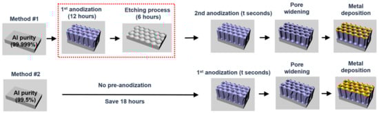
Figure 1.
Comparison of the highly ordered anodic aluminum oxide (HO-AAO) fabrication method (method #1) and the one (QU-AAO) developed in this work (method #2). Method #1 begins with a high purity aluminum substrate (99.999%), followed by two anodization steps and a wet etching procedure between them. Metal deposition is performed either directly after the second anodization process or after pore widening process. On the other hand, method #2 uses an inexpensive aluminum substrate (99.5%) and reduces the two anodization steps into one, removing the etching process, thus finally reducing the minimum fabrication time by 18 h and saving 30 times cost.
Figure 2 shows field emission scanning electron microscopy (FE-SEM) images of the AAO nanostructures developed during the procedures. Throughout the paper, the AAO templates obtained from the two-time anodization process (method #1) are referred to as HO-AAO, while the templates from the single anodization process referred to as QU-AAO (method #2). After the first anodization process, both the HO-AAO and the QU-AAO showed disordered nanopores, but they seem to be quasi-uniform nanopore structures (Figure 2(a-1,b-1)). After the second anodization process, however, only HO-AAO based on the Al with the purity of 99.999% produces close-packed hexagonal nanopore arrays (see Figure 2(a-2,b-2)). This is why the high purity Al substrate is required to obtain the ordered structures. Since QU-AAO does not provide a highly uniform pore array even after the second anodization, we will skip this second anodization process in the use of Al with the low purity of 99.5%. Figure 2(a-3,b-3) display the final plasmonic nanostructures after the gold deposition of 20 nm thickness (without the pore widening process this time). The main differences between the final nanostructures are the pore size and regularity (i.e., highly ordered versus quasi-uniform) in the array pattern.
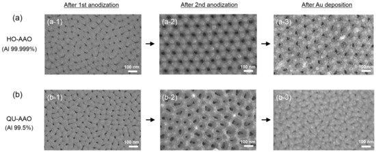
Figure 2.
Field emission scanning electron microscopy (FE-SEM) images of the anodic aluminum oxide (AAO) templates along the fabrication process of two-step anodization and gold deposition procedures. (a) Top-view FE-SEM images for the HO-AAO show irregularly patterned nanopores after the first anodization, but highly ordered hexagonal arrays after the second anodization; (b) Top-view FE-SEM images for the QU-AAO show irregularly patterned nanopores after both the first and second anodization procedures. The FE-SEM images confirm that only the high purity (99.999%) aluminum substrate is possible for forming well-ordered nanopore arrays. The first and second anodization times were 12 h and 60 s, respectively. For all images, scale bar = 100 nm.
We plotted the spectrum as a function of the thickness of the alumina layer, which linearly increases with respect to the anodization time (Figure 3). The growth time for the alumina layer of HO-AAO was higher than that of QU-AAO. The inset shows the FE-SEM cross-section images of QU-AAO. In order to compare the optical properties between HO-AAO and QU-AAO, we used the reflectance spectrum of plasmonic nanostructures in the visible wavelength range, as shown in Figure 4. The layer grows much faster for HO-AAO, presumably due to the fact that the growth occurs in a straighter fashion than QU-AAO. The spectra in Figure 4 show that there are a couple of broad absorption bands in the visible range which shift toward a larger wavelength as the layer becomes thicker (i.e., a red shift), thus changing the color from blue to red (see the color images in Figure 4, which are measured by a camera). The overall spectrum and thickness dependence are almost identical for both of the devices, except that the bands occur at a smaller wavelength for QU-AAO-based nanostructures at a similar thickness (i.e., 70, ~110, and ~140 nm devices). This suggests that by adjusting the thickness of the alumina layer, the plasmonic behaviors based on HO-AAO may be realized with QU-AAO templates.
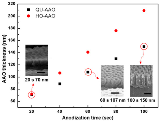
Figure 3.
AAO thickness as a function of anodization time. The thickness increases linearly for both of the templates and HO-AAO (red dot) grows faster than QU-AAO (black dot). Insets are cross-section FE-SEM images for QU-AAO templates. The scale bar was 100 nm.
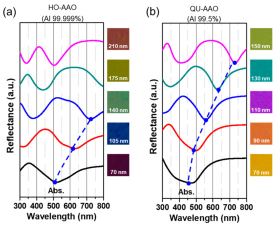
Figure 4.
Optical reflectance spectra of Au-coated (a) HO-AAO and (b) QU-AAO plasmonic nanostructures in visible wavelength range. The spectrum is plotted with respect to the thickness of the alumina layer. The graphs are shifted in the y-axis for clarity according to the alumina thickness. The optical images show the evolution of the sample color. Both AAO plasmonic nanostructures display very similar optical responses, except that the locations of the absorption band are off by 50–100 nm for the samples with the same thickness.
The optical property may also depend on the pore size. At this time, we implement the pore widening process and test the absorbance spectrum as a function of the pore size. Figure 5a,b shows FE-SEM images of the HO-AAO and QU-AAO templates after anodization, pore widening, and gold deposition. For the templates, we perform the widening process for 70 min in phosphoric acid. As seen in Figure 5(a-2,b-2), a highly ordered honeycomb array is obtained for HO-AAO, whose average pore diameter is about 80–85 nm, while nanopores with an irregular pattern and pore diameter are obtained for QU-AAO. Finally, a 20 nm gold layer is deposited on the templates, which could be seen to be accumulated around the rim and bottom of nanopores (Figure 5(a-3,b-3)). The reflectance spectra in Figure 5c show almost identical optical responses and color images between the templates, which would allow dissimilar spectra without the pore widening process. This informs that controlling pore size can also be an effective way to tune the optical properties of the nanostructures. Furthermore, after widening, their optical characteristics could be almost identical due to the similar effective dielectric constant, which can be calculated by the thickness and pore size of AAO. In other words, although the uniformity of pores was broken, their effective dielectric constants, , which were determined by the area ratio (i.e., porosity) between the air and AAO medium (), became similar by widening process, so that their optical behavior could be identical on AAO-based plasmonic nanostructures [38,39,40].
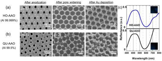
Figure 5.
FE-SEM images and reflectance spectra of (a) HO-AAO and (b) QU-AAO based plasmonic nanostructures after pore widening process. (a-1) and (b-1) display nanopores after the final anodization process; (a-2) and (b-2) are FE-SEM images after the pore widening process for 70 min; (a-3) and (b-3) are images after gold deposition of 20 nm. The anodization times for QU-AAO and HO-AAO were 80 and 60 s, respectively. For all images, scale bar = 100 nm. (c) Reflectance spectra and camera images show almost identical optical properties between the devices.
As shown in Figure 4, the resonance peak shifts towards a longer wavelength as the anodization time increases (i.e., as the layer becomes thicker), where the resonance peak was defined by the plasmonic interference coupled absorption position (see the dot line). The thickness dependence can be understood such that constructive interference occurs at a longer wavelength in a thicker alumina layer. These behaviors were already studied in our previous paper, where absorption peaks were related to the coupling effect of the constructive interference and localized surface plasmon resonance (LSPR) according to the thickness of an alumina layer [38,39,40]. For more quantitative analysis on the pore size dependence, we plotted the resonance peak in the absorption band as a function of the pore widening time for the QU-AAO, with the anodization time of 120 s in Figure 6. The inset in Figure 6b shows the FE-SEM images of the top view for silver coated QU-AAO structures. As the widening time increases, the resonance peaks decreased, which is an opposite trend when compared to the case of thickness. The widening process enlarges the pore, but at the same time reduces the area between the pores (which we call a terrace), where most of the gold is deposited. Therefore, we think that the blue shift of the resonance peak does not result from the increase in pore diameter (i.e., a decreasing effective dielectric constant) but from the decrease in terrace area. Through the combination of varying the layer thickness and pore size, we can effectively control the optical properties of AAO devices in much more cost-efficient ways.
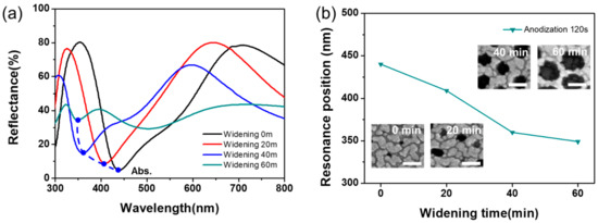
Figure 6.
Absorption resonance behaviors as a function of pore widening time (tW) for QU-AAO based plasmonic structures. (a) The reflectance spectra for different widening times, where the dot line shows the position of absorption resonance peaks; (b) The resonance peak shifts toward shorter wavelength (blue shift) as the pore size increases (longer widening time). The insets showed FE-SEM images of the top view for the silver-coated QU-AAO structures. The scale bar is 100 nm.
Gold, silver, and copper are typical coating materials that are widely used in plasmonic applications [41,42,43,44]. While gold is more stable in air than the other materials, silver provides better absorption than gold at certain wavelengths, and copper is the most cost-effective of the materials. We tested the effect of different coating materials on the optical properties of QU-AAO templates with various alumina thickness without the pore widening process. Figure 7a exhibits the reflectance spectra in the case of silver (solid lines) and gold (dashed lines). The spectra look similar to each other, except that the absorption bands of silver occur at shorter wavelength of ~100 nm relative to gold, where the difference becomes smaller as the alumina layer becomes thicker. On the other hand, the reflectance spectra of copper (solid lines) and gold (dashed lines) in Figure 7b show almost identical wavelength dependence. The differences in Figure 7 are commonly observed in reflectance measurements on these materials which result from the absorption occurring at similar wavelengths for gold and copper, but at shorter wavelength of ~100 nm for silver.
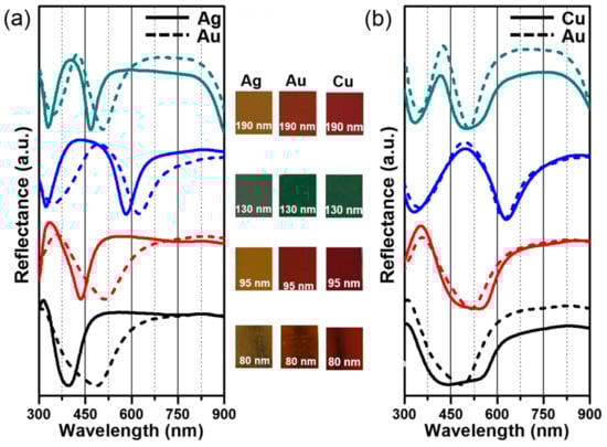
Figure 7.
Comparison of three coating materials: Gold (Au), silver (Ag), and copper (Cu). (a) Optical reflectance spectra and photographs at different alumina thickness are plotted for the comparison between the QU-AAO coated with Au (dashed lines) and Ag (solid lines). The absorption bands of Ag occur at shorter wavelength of ~100 nm relative to Au and the difference becomes smaller as the layer becomes thicker; (b) reflectance measurements of Au (dashed lines) and Cu (solid lines) show almost identical optical properties. The graphs are shifted in the y-axis for clarity.
Figure 8a finally demonstrates that we can realize large-area and flexible plasmonic nanostructures in a cost-efficient way with copper. We deposited a thin Al film of about 500 nm in thickness on flexible polyethylene terephthalate (PET) and then anodized it to produce a QU-AAO template. We controlled the anodization time to obtain different QU-AAO thicknesses for different optical behaviors. Then, a copper layer of 20 nm thickness was deposited to provide plasmonic effects. As shown in Figure 8b, their optical behaviors are well-tuned according to the anodization time. As mentioned earlier, HO-AAO requires a long etching process and loses much of the Al layer (hundreds of micrometers in thickness). On flexible substrates, we could not process such an etching process because the deposited Al could be normally under micrometer scale. Thus, we needed to understand the optical behaviors using QU-AAO to accomplish flexible plasmonic devices.
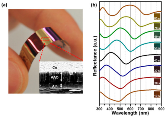
Figure 8.
Photograph of a copper (Cu)-coated QU-AAO template and the corresponding reflectance spectra. (a) Large-area of flexible plasmonic nanostructures can be made with QU-AAO devices developed in this paper. The scale bar is 400 nm. (b) Optical reflectance spectra of the devices as a function of the anodization time (tA). The graphs are shifted in the y-axis for clarity.
To demonstrate the plasmonic effect based on the QU-AAO templates, we conducted SERS measurements with Rhodamine 6G (R6G) dye molecules. Here, we chose silver as the coating material since it typically provides the largest SERS enhancement among the materials discussed above. The QU-AAO templates used for the SERS measurements were obtained with the following conditions: An anodization time of 30 s, a pore widening time of 0 min, and a deposition of a 20 nm Ag layer. For the SERS measurements, we used a laser of 785 nm in wavelength at a 1.33 mW power, exposing the samples to the light for 4 s. We analyzed the SERS intensity as a function of anodization time and pore widening time and found that the intensity is larger at a shorter anodization time and barely depends on the widening time (see Figure 9).
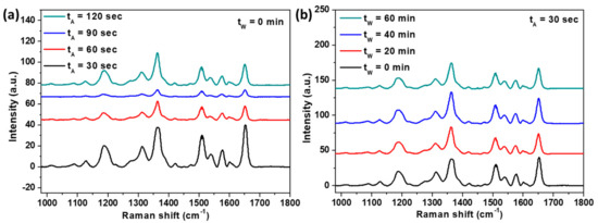
Figure 9.
SERS spectra with R6G dye molecules as a function of (a) anodization time and (b) pore widening time. (a) QU-AAO templates with the widening time of 0 min are used; (b) QU-AAO templates with an anodization time of 30 s are used. The concentration of R6G was 100 µM.
Figure 10 shows the obtained Raman spectrum from the sample of 1 µM R6G on the plasmonic QU-AAO which is compared with the reference spectrum of 10 mM R6G on the Ag-coated silicon substrate. From the three main peaks in the Raman spectrum (1185, 1365, and 1650 cm−1), we can determine the SERS enhancement factor (EF):
where is SERS intensity, is reference Raman intensity, and and are R6G concentration in SERS and Raman solutions [45]. An average EF value of about ~105 was obtained from the measurement and we were able to measure the SERS signal down to a 1 nM molar concentration (see the inset in Figure 10). Therefore, this confirms that the plasmonic QU-AAO can serve as a platform for SERS applications.
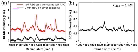
Figure 10.
SERS spectra for enhancement calculation and detection limit. (a) SERS spectra of R6G on Ag coated QU-AAO (the red solid line, CR6G = 1 µM) and on Ag coated Si (the black solid line, CR6G = 10 mM). From the three main peaks in the Raman spectrum (1185, 1365, and 1650 cm−1), we obtained a SERS enhancement factor of ~0.2 × 10⁵. The fabrication conditions for the HU-AAO are an anodization time of 30 s, a pore widening time of 0 min, and the deposition of a 20 nm Ag layer; (b) SERS spectrum for 1 nM R6G on Ag coated QU-AAO.
4. Conclusions
In this paper, we have clearly demonstrated the optical behaviors of large-area, low-cost, and high-throughput QU-AAO-based plasmonic nanostructures. Their plasmonic resonances could almost be considered similar with HO-AAO based plasmonic nanostructures. On the other hand, we were able to save a total time of 18 h and cost by 30 times with the QU-AAO templates when compared to HO-AAO templates, which require a long anodization and etching process and expensive high purity Al (99.999%). Optical reflectance measurements verified that we could effectively tune the optical properties of QU-AAO-based plasmonic nanostructures by changing the thickness of the alumina layer and the diameter of nanopores. Finally, we could demonstrate large-area, flexible, low-cost plasmonic nanostructures on flexible platform. Therefore, QU-AAO templates could provide an effective platform for cost-effective, high-throughput, and large-area AAO-based tunable plasmonic nanostructures that could be applied in various industrial biosensing and photocatalyst applications.
Author Contributions
Conceptualization, D.L. and D.C.; Methodology, Y.B., D.L. and D.C.; Software, Y.B.; Validation, D.L. and D.C.; Formal Analysis, Y.B.; Investigation, J.Y. and Y.J.; Data Curation, Y.B.; Writing—Original Draft Preparation, D.C.; Writing—Review and Editing, D.C.; Visualization, J.Y. and Y.J.; Supervision, D.L. and D.C.; Project Administration, D.C.; Funding Acquisition, D.L. and D.C.
Funding
This research was funded by National Research Foundation of Korea (2017R1A2B2008419) and Korea University Future Research Grant (K1720551).
Conflicts of Interest
The authors declare no conflict of interest.
References
- Barbillon, G. Fabrication and SERS performances of metal/Si and metal/ZnO nanosensors: A review. Coatings 2019, 9, 86. [Google Scholar] [CrossRef]
- Maier, S.A.; Brongersma, M.L.; Kik, P.G.; Meltzer, S.; Requicha, A.A.G.; Atwater, H.A. Plasmonics-a route to nanoscale optical devices. Adv. Mater. 2001, 13, 1501–1505. [Google Scholar] [CrossRef]
- Zhang, N.M.Y.; Li, K.; Shum, P.P.; Yu, X.; Zeng, S.; Wu, Z.; Wang, Q.J.; Yong, K.T.; Wei, L. Hybrid graphene/gold plasmonic fiber-optic biosensor. Adv. Mater. Technol. 2017, 2, 1600185. [Google Scholar] [CrossRef]
- Ren, K.; Gan, Y.X.; Young, T.J.; Moutassem, Z.M.; Zhang, L. Photoelectrochemical responses of doped and coated titanium dioxide composite nanotube anodes. Compos. Part B Eng. 2013, 52, 292–302. [Google Scholar] [CrossRef]
- Xu, S.; Cao, Y.; Zhou, J.; Wang, X.; Xu, W. Plasmonic enhancement of fluorescence on silver nanoparticle films. Nanotechnology 2011, 22, 275715. [Google Scholar] [CrossRef] [PubMed]
- Ahmadivand, A.; Gerislioglu, B. Directional toroidal dipoles driven by oblique poloidal and loop current flows in plasmonic meta-atoms. J. Phys. Chem. C 2018, 122, 24304–24308. [Google Scholar] [CrossRef]
- Fleischman, D.; Fountaine, K.T.; Bukowsky, C.R.; Tagliabue, G.; Sweatlock, L.A.; Atwater, H.A. High spectral resolution plasmonic color filters with subwavelength dimensions. ACS Photon. 2019, 6, 332–338. [Google Scholar] [CrossRef]
- Yun, J.; Lee, H.; Mun, C.; Jahng, J.; Morrison, W.A.; Nowak, D.B.; Song, J.-H.; Kim, D.-K.; Bae, T.-S.; Kim, H.M.; et al. Fabrication and near-field visualization of a wafer-scale dense plasmonic nanostructured array. RSC Adv. 2018, 8, 6444–6451. [Google Scholar] [CrossRef]
- Brongersma, M.L.; Halas, N.J.; Nordlander, P. Plasmon-induced hot carrier science and technology. Nat. Nanotechnol. 2015, 10, 25–34. [Google Scholar] [CrossRef]
- Zhou, Q.; Meng, G.; Liu, J.; Huang, Z.; Han, F.; Zhu, C.; Kim, D.-J.; Kim, T.; Wu, N. A hierarchical nanostructure-based surface-enhanced Raman scattering sensor for preconcentration and detection of antibiotic pollutants. Adv. Mater. Technol. 2017, 2, 1700028. [Google Scholar] [CrossRef]
- He, J.; Villa, N.S.; Luo, Z.; An, S.; Shen, Q.; Tao, P.; Song, C.; Wu, J.; Deng, T.; Shang, W. Integrating plasmonic nanostructures with natural photonic architectures in Pd-modified morpho butterfly wings for sensitive hydrogen gas sensing. RSC Adv. 2018, 8, 32395–32400. [Google Scholar] [CrossRef]
- Lee, S.; Lee, M.H.; Shin, H.J.; Choi, D. Control of density and LSPR of Au nanoparticles on graphene. Nanotechnology 2013, 24, 275702–275708. [Google Scholar] [CrossRef]
- Gerislioglu, B.; Ahmadivand, A.; Pala, N. Functional quadrumer clusters for switching between Fano and charge transfer plasmons. IEEE Photon. Technol. Lett. 2017, 29, 2226–2229. [Google Scholar] [CrossRef]
- Naik, G.V.; Shalaev, V.M.; Boltasseva, A. Alternative plasmonic materials: beyond gold and silver. Adv. Mater. 2013, 25, 3264–3294. [Google Scholar] [CrossRef]
- Guler, U.; Shalaev, V.M.; Boltasseva, A. Nanoparticle plasmonics: Going practical with transition metal nitirdes. Mater. Today 2015, 18, 227–237. [Google Scholar] [CrossRef]
- Kim, S.; Kim, J.M.; Park, J.E.; Nam, J.M. Nonnoble-metal-based plasmonic nanomaterials: Recent advances and future perspectives. Adv. Mater. 2018, 30, 1704528. [Google Scholar] [CrossRef]
- Mueller, A.D.; Tobing, L.Y.M.; Zhang, D.H. Reliable fabrication of high aspect ratio plasmonic nanostructures based on seedless pulsed electrodeposition. Adv. Mater. Technol. 2018, 4, 1800364. [Google Scholar] [CrossRef]
- Agapov, R.L.; Srijanto, B.; Fowler, C.; Briggs, D.; Lavrik, N.V.; Sepaniak, M.J. Lithography-free approach to highly efficient, scalable SERS substrates based on disordered clusters of disc-on-pillar structures. Nanotechnology 2013, 24, 505302. [Google Scholar] [CrossRef] [PubMed]
- Song, J.; Nam, W.; Zhou, W. Scalable high-performance nanolaminated SERS substrates based on multistack vertically oriented plasmonic nanogaps. Adv. Mater. Technol. 2019, 4, 1800689. [Google Scholar] [CrossRef]
- Ahmadivand, A.; Semmlinger, M.; Dong, L.; Gerislioglu, B.; Nordlander, P.; Halas, N.J. Toroidal dipole-enhanced third harmonic generation of deep ultraviolet light using plasmonic meta-atoms. Nano Lett. 2019, 19, 605–611. [Google Scholar] [CrossRef]
- Lee, W.; Park, S.J. Porous anodic aluminum oxide: Anodization and templated synthesis of functional nanostructures. Chem. Rev. 2014, 114, 7487–7556. [Google Scholar] [CrossRef]
- Zhou, L.; Tan, Y.; Wang, J.; Xu, W.; Yuan, Y.; Cai, W.; Zhu, S.; Zhu, J. 3D self-assembly of aluminum nanoparticles for plasmon-enhanced solar desalination. Nat. Photon. 2016, 10, 393–398. [Google Scholar] [CrossRef]
- Sohn, A.; Gwon, M.; Choi, D.; Kim, D.W. Plasmonic coupling in three-dimensional Au nanoparticle assemblies fabricated by anodic aluminum oxide templates. J. Nanomater. 2013, 2013, 1–6. [Google Scholar] [CrossRef]
- Li, J.; Yu, W.; Zheng, D.; Zhao, X.; Choi, C.H.; Sun, G. Hot embossing for whole Teflon superhydrophobic surface. Coatings 2018, 8, 227. [Google Scholar] [CrossRef]
- Hyam, R.S.; Choi, D. Effects of titanium foil thickness on TiO2 nanostructures synthesized by anodization. RSC. Adv. 2013, 3, 7057–7063. [Google Scholar] [CrossRef]
- Wang, S.; Liu, H.; Han, J. Comprehensive study of Au nano-mesh as a catalyst in the fabrication of silicon nanowires arrays by metal-assisted chemical etching. Coatings 2019, 9, 149. [Google Scholar] [CrossRef]
- Gan, Y.; Yu, Z.; Gan, J.; Cheng, W.; Li, M. Gold catalyst-assisted metal organic chemical vapor deposition of Bi–Te–Ni–Cu–Au complex thermoelectric materials on anodic aluminum oxide nanoporous template. Coatings 2018, 8, 166. [Google Scholar] [CrossRef]
- Belushkin, A.; Yesilkoy, F.; Altug, H. Nanoparticle-enhanced plasmonic biosensor for digital biomarker detection in a microarray. ACS Nano 2018, 12, 4453–4461. [Google Scholar] [CrossRef]
- Shen, Y.; Zhou, J.; Liu, T.; Tao, Y.; Jiang, R.; Liu, M.; Xiao, G.; Zhu, J.; Zhou, J.-K.; Wang, X.; et al. Plasmonic gold mushroom arrays with refractive index sensing figures of merit approaching the theoretical limit. Nat. Commun. 2013, 4, 2381. [Google Scholar] [CrossRef]
- Jia, P.; Jiang, H.; Sabarinathan, J.; Yang, J. Plasmonic nanohole array sensors fabricated by template transfer with improved optical performance. Nanotechnology 2013, 24, 195501. [Google Scholar] [CrossRef]
- Bruera, F.A.; Kramer, G.R.; Vera, M.L.; Ares, A.E. Synthesis and morphological characterization of nanoporous aluminum oxide films by using a single anodization step. Coatings 2019, 9, 115. [Google Scholar] [CrossRef]
- Zhou, Q.; Meng, G.; Huang, Q.; Zhu, C.; Tang, H.; Qian, Y.; Chen, B.; Chen, B. Ag-nanoparticles-decorated NiO-nanoflakes grafted Ni-nanorod arrays stuck out of porous AAO as effective SERS substrates. Phys. Chem. Chem. Phys. 2014, 16, 3686–3692. [Google Scholar] [CrossRef] [PubMed]
- Shan, D.; Huang, L.; Li, X.; Zhang, W.; Wang, J.; Cheng, L.; Feng, X.; Liu, Y.; Zhu, J.; Zhang, Y. Surface plasmon resonance and interference coenhanced SERS substrate of AAO/Al-based Ag nanostructure arrays. J. Phys. Chem. C 2014, 118, 23930–23936. [Google Scholar] [CrossRef]
- Le Ru, E.C.; Blackie, E.; Meyer, M.; Etchegoin, P.G. Surface enhanced Raman scattering enhancement factors: A comprehensive study. J. Phys. Chem. C 2007, 111, 13794–13803. [Google Scholar] [CrossRef]
- Yao, Z.; Wang, C.; Li, Y.; Kim, N.Y. AAO-assisted synthesis of highly ordered, large-scale TiO2 nanowire arrays via sputtering and atomic layer deposition. Nanoscale Res. Lett. 2015, 10, 166. [Google Scholar] [CrossRef] [PubMed][Green Version]
- Yin, A.J.; Li, J.; Jian, W.; Bennett, A.J.; Xu, J.M. Fabrication of highly ordered metallic nanowire arrays by electrodeposition. Appl. Phys. Lett. 2001, 79, 1039–1041. [Google Scholar] [CrossRef]
- Zhang, C.; Li, W.; Yu, D.; Wang, Y.; Yin, M.; Wang, H.; Song, Y.; Zhu, X.; Chang, P.; Chen, X.; et al. Wafer-scale highly ordered anodic aluminum oxide by soft nanoimprinting lithography for optoelectronics light management. Adv. Mater. Interfaces 2017, 4, 1601116. [Google Scholar] [CrossRef]
- Choi, D.; Shin, K.S.; Yoon, D.; Chung, D.S.; Jin, Y.W.; Lee, L.P. Plasmonic optical interference. Nano Lett. 2014, 14, 3374–3381. [Google Scholar] [CrossRef]
- Jo, H.; Yoon, D.; Sohn, A.; Kim, D.-W.; Choi, Y.; Kang, T.; Choi, D.; Kim, S.-W.; Lee, L.P. Asymmetrically coupled plasmonic core and nanotriplet satellites. J. Phys. Chem. C 2014, 118, 18659–18667. [Google Scholar] [CrossRef]
- Choi, D.; Choi, Y.; Hong, S.; Kang, T.; Lee, L.P. Self-organized hexagonal-nanopore SERS array. Small 2010, 16, 1741–1744. [Google Scholar] [CrossRef]
- Hu, M.; Chen, J.; Li, Z.Y.; Au, L.; Hartland, G.V.; Li, X.; Marquez, M.; Xia, Y. Gold nanostructures: Engineering their plasmonic properties for biomedical applications. Chem. Soc. Rev. 2006, 35, 1084–1094. [Google Scholar] [CrossRef] [PubMed]
- Kravets, V.G.; Jalil, R.; Kim, Y.J.; Ansell, D.; Aznakayeva, D.E.; Thackray, B.; Britnell, L.; Belle, B.D.; Withers, F.; Radko, I.P.; et al. Graphene-protected copper and silver plasmonics. Sci. Rep. 2014, 4, 5517. [Google Scholar] [CrossRef]
- Guay, J.M.; Killaire, G.; Gordon, P.G.; Barry, S.T.; Berini, P.; Weck, A. Passivation of plasmonic colors on bulk silver by atomic layer deposition of aluminum oxide. Langmuir 2018, 34, 4998–5010. [Google Scholar] [CrossRef] [PubMed]
- Wes, P.R.; Ishii, S.; Naik, G.V.; Emani, N.K.; Shalaev, V.M.; Boltasseva, A. Searching for better plasmonic materials. Laser Photon. Rev. 2010, 4, 795–808. [Google Scholar] [CrossRef]
- Hildebrandt, P.; Stockburger, M. Surface-enhanced resonance Raman spectroscopy of Rhodamine 6G adsorbed on colloidal silver. J. Phys. Chem. 1984, 88, 5395–5944. [Google Scholar] [CrossRef]
© 2019 by the authors. Licensee MDPI, Basel, Switzerland. This article is an open access article distributed under the terms and conditions of the Creative Commons Attribution (CC BY) license (http://creativecommons.org/licenses/by/4.0/).