Abstract
The rectifying characteristics of a Mo/SiC Schottky contact fabricated by facing targets sputtering system were investigated through current–voltage measurement. The Schottky diode parameters were extracted from the forward current–voltage characteristic curve by the Cheung and Cheung method and the Norde method. The as-deposited Mo/SiC Schottky contacts possessed Schottky barrier heights of 1.17 and 1.22 eV, respectively. The Schottky barrier heights of the diodes were decreased to 1.01 and 0.91 eV after annealing at 400 °C for 30 min. The ideality factor was increased from 1.14 and 1.08 to 1.51 and 1.41, respectively. This implies the presence of non-ideal behaviors due to a current transport mechanism other than ideal thermionic emission, and the non-ideal behaviors increased as a result of excessive thermal annealing. In contrast, only a negligible change was observed in the crystallographic characteristics. This result suggests that the reason for the deviation from the ideal rectifying characteristics of the Mo/SiC Schottky contact through the annealing process was the variation in the current transport mechanism, including recombination, tunneling, and/or minority carrier injection.
1. Introduction
In recent decades, remarkable progress has been made in the field of power electronics. Silicon is, by far, the most used material in power electronics; however, performance improvements are restricted by the limited inherent characteristics of Si [1]. Silicon carbide (SiC), which is an indirect energy-gap semiconductor, is the most promising material for next-generation power semiconductor devices and could also be an attractive alternative to silicon with superior properties in the field of power electronics. Gallium nitride (GaN), which is a direct energy-gap semiconductor, is also one of the representative materials in power electronics field. However, SiC has higher thermal conductivity than GaN; thus, SiC is regarded as a promising material in power electronics field. SiC possesses superior characteristics compared to Si, including high thermal conductivity (4.9 W/cm∙K), dielectric breakdown field (2.5 mV/cm), saturated electron velocity (2 × 107 cm/s), and wide band-gap energy (3.26 eV). The outstanding thermal properties and wide band-gap energy could allow SiC devices to be operated under harsh environments, such as high-temperature conditions [2]. Furthermore, SiC-based power electronic devices could achieve considerably higher voltage-blocking capacities with a smaller size, owing to their excellent electrical properties [3].
With these exceptional features, SiC is a very acceptable compound semiconductor for the base material of unipolar devices such as Schottky-barrier diodes (SBDs) and metal-oxide semiconductor field-effect transistors [4]. As the simplest structure among unipolar devices, SBD has engaging power electronics applications. Because of its low forward-voltage drop and fast switching behavior, SBD has been widely researched and used. In the case of Si, however, the voltage-blocking capacity of SBDs is limited by the trade-off relationship between the resistance and doping level of the drift region. Consequently, the operating voltage of the Si SBD is limited to less than a few hundred volts [5,6]. Meanwhile, the demands of the fast-switching rectifier in the field of high-voltage applications, beyond the limitation of the Si SBD operation range, remains under consideration. Because these demands cannot be met by Si SBDs, research on SiC SBDs is becoming more important. For the case of equal voltage-blocking capacity, SiC SBD (4H polytype) could offer 100 times lower resistance than that of the Si SBD [7]. In other words, SiC SBDs could obtain significantly higher voltage grading than Si SBDs at an equal resistance condition.
The rectifying nature of the SiC SBD stems from the Schottky contact between the metal and SiC and could be evaluated in terms of the magnitude of the Schottky barrier height (SBH) at the junction. SiC forms a Schottky rectifying contact with the metal with a sufficiently large work function. According to the Schottky–Mott relationship, the magnitude of the SBH (ΦB) could be roughly predicted by the difference between the work function of the metal (ΦMetal) and the electron affinity of the semiconductor (χSemi) [7].
However, there is a discrepancy between the experimentally measured SBH and the predicted value. This indicates that the SBH of practical devices is dependent on not only simple theory but also other effects. For these phenomena, the existence of the interfacial layer between the metal and semiconductor has an influence [8]. Based on this concept, many kinds of metals and alloys have been adopted as the Schottky metal in the SiC SBD structure [9,10,11,12,13]. Among the kinds of Schottky metals, Ti and Ni are the most frequently utilized metals, and for the contact with n-type 4H–SiC, their SBH values are predicted to be approximately 0.9 and 1.6 eV, respectively, by the Schottky–Mott relationship. Generally, as an indicator of the off-state performance, the reverse current is inversely proportional to the SBH. A device with a small value of SBH shows better on-state behavior. By analogy with this tendency, a junction having moderate SBH could be applied to a device that has the balanced performance at the on and off states. Nakamura et al. suggested that the Schottky contact with an SBH of 1.2–1.3 eV is imperative for the fabrication of a high-efficiency and high-voltage 4H–SiC SBD [13].
Mo is a kind of refractory metal with a work function of about 4.6 eV, and a Mo/SiC Schottky contact could achieve an SBH of 1.2 eV. Furthermore, attaining the optimum SBH at contact is feasible by controlling the properties of the interfacial layer between the Mo/SiC contacts. In this work, the Mo/SiC Schottky contacts were fabricated using the facing targets sputtering (FTS) system (Figure 1). FTS system is different with conventional sputtering method, and it can fabricate a high-quality film. During the deposition, a plasma region is formed between the two facing targets in this system, and the substrate is placed away from where the plasma is formed. From this unusual structure, several advantages could be derived. In the plasma region, the charged particles that form and sustain the plasma discharge are concentrated by the magnetic field. Consequently, spiral-shaped high-density plasma is constructed. As a result, stable discharging under low-pressure/temperature conditions could be continued and the uniformity of thin films could be improved. In addition, the damage to the substrate and the previously deposited thin film could be prevented by restriction of the energetic charged particles [14,15,16]. These features affected the work function of fabrication of multilayer-structured devices using SiC substrate. Additionally, post-thermal annealing was induced to prepare samples with the purpose of observing the effect of annealing temperature on the SBH of the contact.
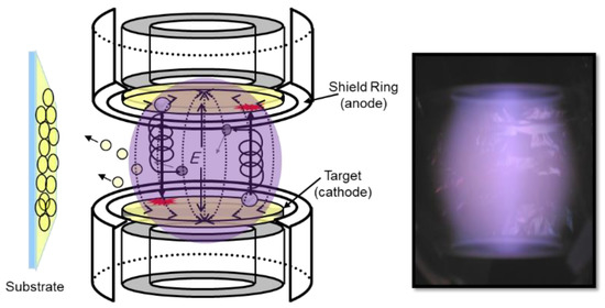
Figure 1.
Schematic of the facing targets sputtering system.
2. Materials and Methods
The SiC wafer used in this study was n-type 4H–SiC polytype and the magnitude of the net doping level was 5 × 10¹⁵/cm3. The back-side ohmic contact was a structure of Ni/Ti/NiV/Ag (Figure 2). SiC wafer was ultrasonically cleaned in acetone, deionized water and ethyl alcohol for 10 min to remove impurities on the substrate surface. Then, the SiC wafer was dried with nitrogen gas. Mo (4N purity, 4 inch diameter, 1/4 inch thick) was used as the Schottky contact metal and Al (4N purity, 4 inch diameter, 1/4 inch thick) was used as the pad metal in this study. In the deposition process, Mo and Al thin films were deposited onto the SiC wafer sequentially by the facing targets sputtering method under in-situ conditions. The thickness of the Mo and Al thin films was 1000 and 3000 Å, respectively, and the active area on which the metal was deposited was 0.36 mm2. Details for deposition conditions are shown in Table 1. After the deposition, the samples were thermally annealed at a temperature range of 300–400 °C for 10–30 min under Ar ambient by tubular furnace (BY-300, Buyoung, Seoul, Korea). The Schottky characteristics of the prepared samples were measured using an J–V (Current density-voltage) curve tracer (2410 SMU, Keithley, Solon, OH, USA,) at room temperature. The crystallographic analysis was also performed with X-ray diffraction (XRD, D-max 2200, Rigaku, Tokyo, Japan) measurement with Cu Kα radiation (λ = 1.5418Å) at the scanning angle (2θ) of 20°–80°.
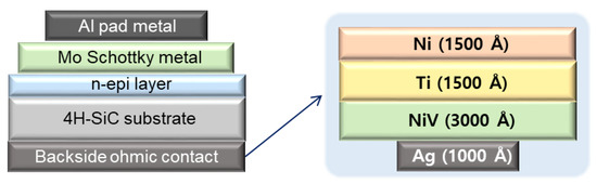
Figure 2.
Structure of as-fabricated Mo/SiC Schottky diode.

Table 1.
Deposition conditions.
3. Results
The forward and reverse J–V characteristic curves of the Mo/SiC Schottky contacts that were thermally annealed under various condition are shown in Figure 3. For both annealing times, the forward voltage was shifted toward a lower voltage after annealing. The magnitude of this shift showed a proportional trend to the increment in the annealing temperature and time. The reverse current of the samples was not changed significantly, regardless of annealing times. To perform the quantitative evaluation for the electrical properties of prepared samples, the Schottky diode parameters of the samples were calculated from the forward J–V characteristic curve through Cheung and Cheung’s method [17]. Through this method, it is possible to extract Schottky diode parameters, such as the SBH (φB), series resistance (RS), and ideality factor (n), from two different linear plots that were modified from a single measured J–V curve. The equations of these plots are
and the resulting plots are displayed in Figure 4. In this calculation, the constants k, q and A** indicate the Boltzmann’s constant, the charge of an electron, and Richardson’s constant, respectively. The theoretical value of Richardson's constant is regarded as 146 A/cm2∙K2 for 4H–SiC [18]. In Figure 4a, the y-intercept of each plot is denoted by nkT/q, and, from this point, the ideality factor of each diode could be determined. The nonlinear section of these plots implies the non-ideal behavior of diodes in the low-voltage region. The plot of the function d(H) could be graphed with the left side and analyzed with the right side of the equation. From the y-intercept and the slope of this plot, the SBH and series resistance could be calculated, respectively. For the purpose of a comparative analysis between each method, the Norde method was also employed for the calculation of the device parameters [19,20].
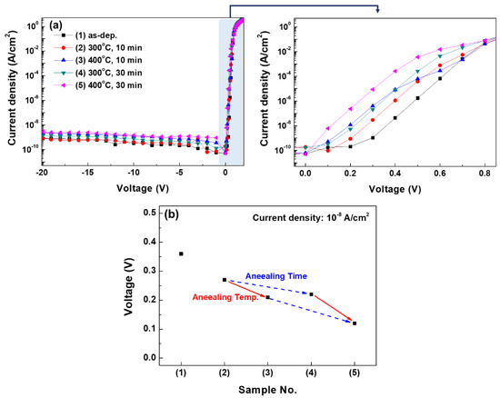
Figure 3.
Typical forward and reverse J–V characteristic curves of Mo/SiC Schottky contacts with various annealing conditions: (a) J–V characteristic curves; (b) change of forward voltage by annealing temperature and time (current density = 10−8 A/cm2).
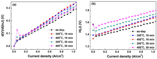
Figure 4.
Plots calculated by the Cheung and Cheung method equation for Mo/SiC Schottky contacts: (a) dV/d(ln J) vs. J; (b) H(J) vs. J.
In this method, the function defined by Norde [19] and modified by Bohlin [20],
is used and its plot is shown in Figure 5.
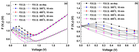
Figure 5.
Norde plots of the Mo/SiC Schottky contacts with various annealing conditions: (a) 0–2.0 V; and (b) 0–0.75 V.
The arbitrary constant γ should be determined to be greater than the ideality factor, and the values used in this calculation were 2 and 3. With the minimum point of each plot with two different γ values, two simultaneous equations were determined and the parameters were calculated from the solution of these equation.
Figure 6 and Table 2 show the Schottky diode parameters calculated by the Cheung and Cheung [17] and Norde [19] methods. As a result of comparing these methods, the variation in the Schottky diode parameters as a function of the annealing temperature and time indicated a similar tendency. As shown in Figure 6, the SBH slightly decreased based on the thermal annealing temperature and time. These results are in agreement with the tendency in the variation in the reverse current and the forward voltage. The magnitude of the SBH plays a crucial role in determining the reverse current. From the Schottky diode equation, which is based on the thermionic emission theory, it is implied that the reverse current at the reverse blocking condition is in exponentially reciprocal proportion to the SBH [5].
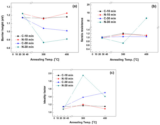
Figure 6.
Summarized plot of the parameters of prepared Schottky diodes using the Cheung and Cheung method and the Norde method: (a) barrier height; (b) Series resistance; and (c) ideality factor.
Table 2.
Summarized device parameters of prepared Schottky diodes.
The relation between forward voltage with SBH could also be indicated by this equation. When a forward bias is applied to the device, the exponential term in the square brackets of the equation becomes the dominant component of the current flow [21]. In this circumstance, the forward voltage, the inflexion point of forward I-V characteristic curve, is shifted to a lower voltage by the decrease in the SBH. The ideality factor of the as-deposited sample calculated by each method was 1.15 and 1.09. For the group of samples that were annealed for 10 min, no significant change was observed in terms of the ideality factor. In the general case, the ideality factor of the practical diodes has a value between 1 and 2. An ideality factor of approximately 1 indicates that the diode has nearly ideal behavior and the thermionic emission model is the dominant transport mechanism in the diode.
In contrast, slight increases and further increases of the ideality factor were found in samples that were annealed for 30 min. The deviation in the ideality factor from 1 means the diodes had an inhomogeneous effect on the SBH and/or the presence of an interfacial layer [22,23]. A non-ideal transport mechanism other than the ideal thermionic emission current, such as the minority carrier injection from the metal into the semiconductor and/or the quantum mechanical tunneling through the potential barrier, could also be a reason for this deviation [21]. From this result, it is possible to anticipate that a moderate annealing condition could impact the improvement in the rectifying performance of the SBD, whereas excessive annealing, such as that with immoderately high temperature and long time, could cause degradation of the device. This result also suggests that the moderate annealing condition for the Mo/SiC Schottky contact is that of 300 °C and 10 min. To identify the changes in the crystallographic characteristics of the interfacial layer of the Mo/SiC SBD structure from thermal annealing, the XRD measurement was executed.
Figure 7 shows the XRD patterns of the bare SiC wafer and prepared Mo/SiC Schottky diodes. Each spectrum was normalized to the highest peak intensity. The characteristic peaks near 43.8° and 63.8° were detected in the entire spectra. These could be characterized as Al0.5Fe0.5 peaks, and may have arisen from the sample holder of the measuring equipment. In addition, near 35°, substantial peaks were detected in all spectra. It is supposed that this peak is the 4H–SiC characteristic peak, which is reinforced by the convolution of two peaks, 4H–SiC (101) peak and 4H–SiC (004) [24,25]. Broad peaks placed over the 2θ range of 73°–80° were also observed, and these could be assumed to be a convolution of peaks exhibiting 4H–SiC, as in the case of the peaks near 35°. However, only a small narrow peak was found in this 2θ range at the XRD patterns of the sample that was annealed at 400 °C for 10 min. This difference between the spectra may be due to the difference in measurement conditions. To correct the position of the sample, a proper 2θ offset was applied during the execution of the measurement. Its proper value was distinguished for each case, and this variation in measurement conditions could cause the difference between spectra. In contrast with the bare SiC, the spectra of SBDs exhibit characteristic peaks at 39.7°, which could be assumed to be the silicide phase that formed between the Mo/SiC interfacial layers. A noticeable increase or decrease in the intensity of these peaks was not present through the annealing process. The interfacial layer is commonly supposed to have a thickness of a few angstroms [8]. By this assumption, the XRD patterns imply that the formation of the molybdenum silicide phase occurred during the Mo deposition of first few angstroms. It could also imply that the formation of the molybdenum silicide phase was largely independent of the thermal annealing process.
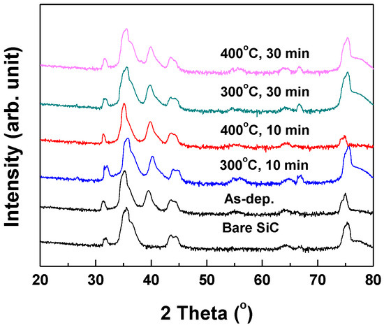
Figure 7.
XRD patterns of the Mo/SiC Schottky contact.
4. Conclusions
The thermal annealing effect on Mo/SiC Schottky contacts was investigated. The calculated magnitude of the Schottky barrier heights of the as-deposited diode were 1.17 and 1.22 eV. After thermal annealing of the samples, a slight decrease in the SBH was observed, which was proportional to the annealing temperature and the time of application. Depending on the narrowing of the SBH, the forward voltage at the forward-conducting condition was shifted to a lower voltage. When the diode exhibited a reverse blocking behavior, the reverse current of the diode increased for the same reason. With higher heat energy transferred to the samples during the annealing process by a higher temperature and longer time, the ideality factors of the diodes deviated from 1. This indicates that annealing under excessive conditions could cause deterioration of the rectifying performance of the diode and the loss of ideal behavior. From the result of crystallographic analysis by the X-ray diffraction technique, noticeable changes were not detected. This implies that the change in the SBH and electrical properties of the Mo/SiC Schottky contact was mainly dependent on the variation in the other current transport mechanisms, rather than on the thermionic emission current. From this result, the Mo/SiC Schottky barrier diode is an attractive rectifying device, and it was suggested that the moderate annealing condition for this structure is at 300 °C for 10 min. Furthermore, improved Mo/SiC Schottky power device performance could be obtained by applying not only the structural improvement as the traditional method, including the junction-edge termination and guard ring, but also the post-thermal annealing process with the optimized conditions suggested in this work.
Author Contributions
Conceptualization, J.H. and K.H.K. (Kyung Hwan Kim); methodology, K.H.K. (Ki Hyun Kim); formal analysis, K.H.K. (Ki Hyun Kim); investigation, J.H. and K.H.K. (Ki Hyun Kim); writing—review and editing, J.H. and K.H.K. (Kyung Hwan Kim)
Funding
This research was supported by Basic Science Research Program through the National Research Foundation of Korea (NRF) funded by the Ministry of Education (NRF-2018R1D1A1A02086163).
Conflicts of Interest
The authors declare no conflict of interest.
References
- Itoh, A.; Kimoto, T.; Matsunami, H. High performance of high-voltage 4H–SiC Schottky barrier diodes. IEEE Electron Dev. Lett. 1995, 16, 280–282. [Google Scholar] [CrossRef]
- Sriram, S.; Siergiej, R.R.; Clarke, R.C.; Agarwal, A.K.; Brandt, C.D. SiC for Microwave Power Transistor. Phys. Status Solidi 1997, 162, 441–457. [Google Scholar] [CrossRef]
- Singh, R.; Cooper, J.A.; Melloch, M.R.; Chow, T.P.; Palmour, J.W. SiC power Schottky and PiN diodes. IEEE Trans. Electron Dev. 2002, 49, 665–672. [Google Scholar] [CrossRef]
- Baliga, B.J. Silicon Carbide Power Devices; World Scientific: Singapore, 2006. [Google Scholar]
- Baliga, B.J. Advanced Power Rectifier Concepts; Springer: Boston, MA, USA, 2009. [Google Scholar]
- Buttay, C.; Planson, D.; Allard, B.; Bergogne, D.; Bevilacqua, P.; Joubert, C.; Lazar, M.; Martin, C.; Morel, H.; Tournier, D.; et al. State of the art of high temperature power electronics. Mater. Sci. Eng. B 2011, 176, 283–288. [Google Scholar] [CrossRef]
- Baliga, B.J. The future of power semiconductor device technology. Proc. IEEE 2001, 89, 822–832. [Google Scholar] [CrossRef]
- Cowley, A.M.; Sze, S.M. Surface states and barrier height of metal-semiconductor systems. J. Appl. Phys. 1965, 36, 3212–3220. [Google Scholar] [CrossRef]
- Kim, D.H.; Lee, J.H.; Moon, J.H.; Oh, M.S.; Song, H.K.; Yim, J.H.; Lee, J.B.; Kim, H.J. Improvement of the reverse characteristics of Ti/4H–SiC Schottky barrier diodes by thermal treatments. Solid State Phenom. 2007, 124–126, 105–108. [Google Scholar] [CrossRef]
- Schoen, K.J.; Henning, J.P.; Woodall, J.M.; Cooper, J.A.; Melloch, M.R. A dual-metal-trench Schottky pinch-rectifier in 4H–SiC. IEEE Electron Dev. Lett. 1998, 19, 97–99. [Google Scholar] [CrossRef]
- Gupta, S.K.; Azam, A.; Akhtar, J. Improved electrical parameters of vacuum annealed Ni/4H–SiC (0 0 0 1) Schottky barrier diode. Phys. B Condens. Matter 2011, 406, 3030–3035. [Google Scholar] [CrossRef]
- Vassilevski, K.V.; Nikitina, I.P.; Bhatnagar, P.; Horsfall, A.B.; Wright, N.G.; O’Neill, A.G.; Uren, M.J.; Hilton, K.P.; Munday, A.G.; Hydes, A.J.; et al. High Temperature operation of Silicon Carbide Schottky diodes with recoverable avalanche breakdown. Mater. Sci. Forum 2006, 527–529, 931–934. [Google Scholar] [CrossRef]
- Nakamura, T.; Miyanagi, T.; Kamata, I.; Jikimoto, T.; Tsuchida, H. A 4.15 kV 9.07-m/spl Omega//spl middot/cm/sup 2/4H–SiC Schottky-barrier diode using Mo contact annealed at high temperature. IEEE Electron Dev. Lett. 2005, 26, 99–101. [Google Scholar] [CrossRef]
- Kim, K.H.; Son, I.H.; Song, K.B.; Kong, S.H.; Keum, M.J.; Nakagawa, S.; Naoe, M. Thin film properties by facing targets sputtering system. Appl. Surf. Sci. 2001, 169–170, 410–414. [Google Scholar] [CrossRef]
- Zhang, Z.; Hossain, M.F.; Arakawa, T.; Takahashi, T. Facing-target sputtering deposition of ZnO films with Pt ultra-thin layers for gas-phase photocatalytic application. J. Hazard. Mater. 2010, 176, 973–978. [Google Scholar] [CrossRef] [PubMed]
- Jung, Y.S.; Park, Y.S.; Kim, K.H.; Lee, W. Properties of AZO/Ag/AZO multilayer thin film deposited on polyethersulfone substrate. Trans. Electr. Electron. Mater. 2013, 14, 9–11. [Google Scholar] [CrossRef]
- Cheung, S.K.; Cheung, N.W. Extraction of Schottky diode parameters from forward current-voltage characteristics. Appl. Phys. Lett. 1986, 49, 85–87. [Google Scholar] [CrossRef]
- Roccaforte, F.; La Via, F.; Raineri, V.; Pierobon, R.; Zanoni, E. Richardson’s constant in inhomogeneous silicon carbide Schottky contacts. J. Appl. Phys. 2003, 93, 9137–9144. [Google Scholar] [CrossRef]
- Norde, H. A modified forward I-V plot for Schottky diodes with high series resistance. J. Appl. Phys. 1979, 50, 5052–5053. [Google Scholar] [CrossRef]
- Bohlin, K.E. Generalized Norde plot including determination of the ideality factor. J. Appl. Phys. 1986, 60, 1223–1224. [Google Scholar] [CrossRef]
- Baliga, B.J. Fundamentals of Power Semiconductor Devices; Springer: Boston, MA, USA, 2008. [Google Scholar]
- Tung, R. Electron transport at metal-semiconductor interfaces: General theory. Phys. Rev. B 1992, 45, 13509–13523. [Google Scholar] [CrossRef]
- Crowell, C.R. The Richardson constant for thermionic emission in Schottky barrier diodes. Solid State Electron. 1965, 8, 395–399. [Google Scholar] [CrossRef]
- Chow, T.P.; Bower, D.H.; Van Art, R.L.; Katz, W. Proeprties of sputtered Molybdenum Silicide thin films. J. Electrochem. Soc. 1983, 130, 952. [Google Scholar] [CrossRef]
- Zakeri, M.; Ahmadi, M. Effect of starting composition on formation of MoSi2–SiC nanocomposite powder via ball milling. Bull. Mater. Sci. 2012, 35, 533–538. [Google Scholar] [CrossRef]
© 2019 by the authors. Licensee MDPI, Basel, Switzerland. This article is an open access article distributed under the terms and conditions of the Creative Commons Attribution (CC BY) license (http://creativecommons.org/licenses/by/4.0/).