Electrical and Structural Properties of All-Sputtered Al/SiO2/p-GaN MOS Schottky Diode

 , ,
, ,
Abstract
:1. Introduction
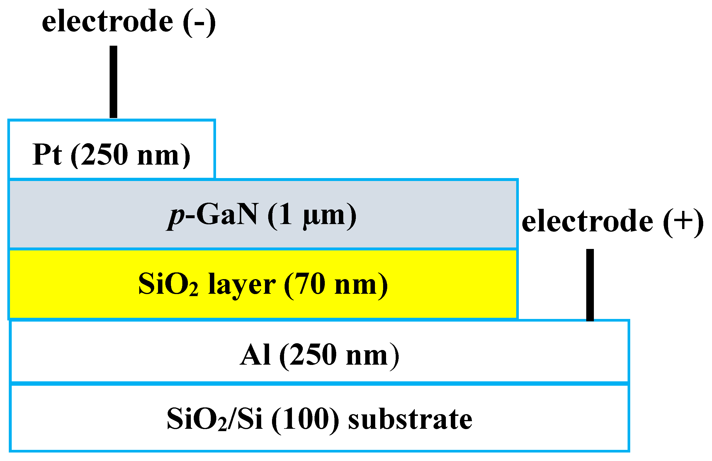
2. Materials and Methods
3. Results and Discussion
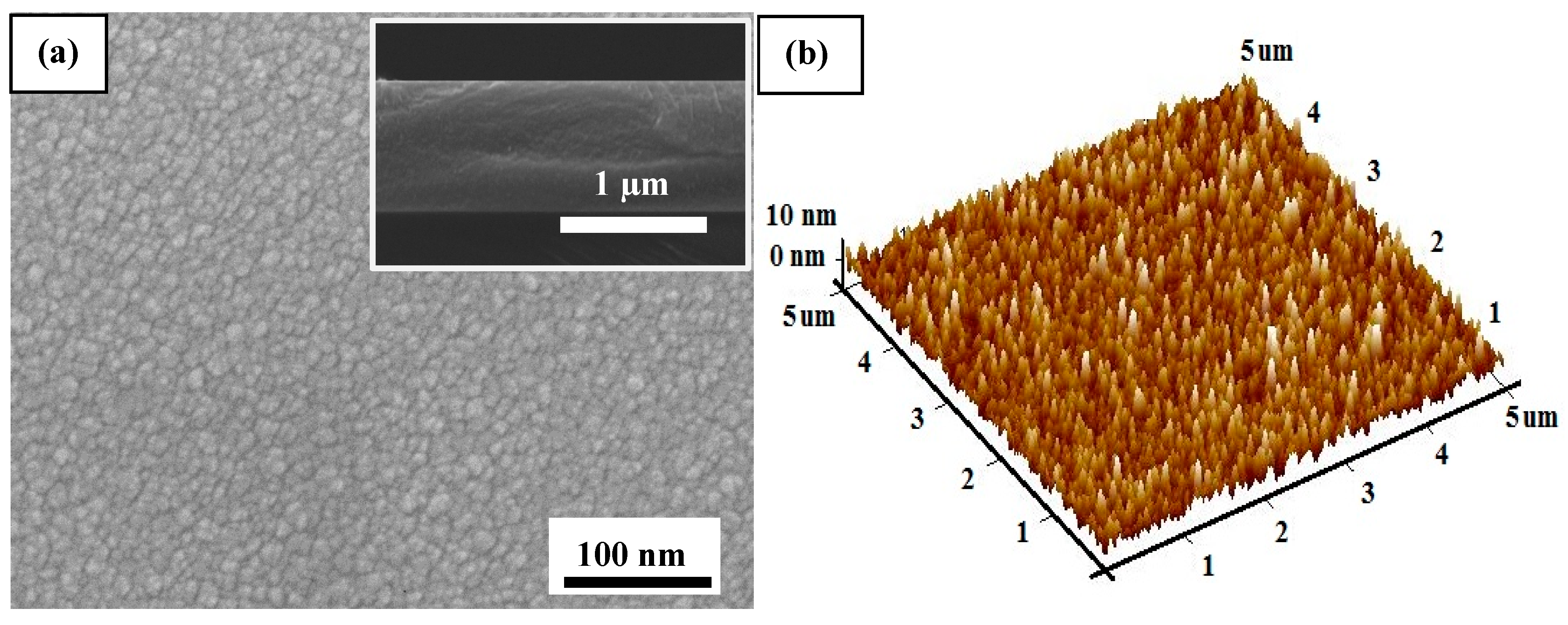
3.1. Structural and Surface Morphological Characteristics
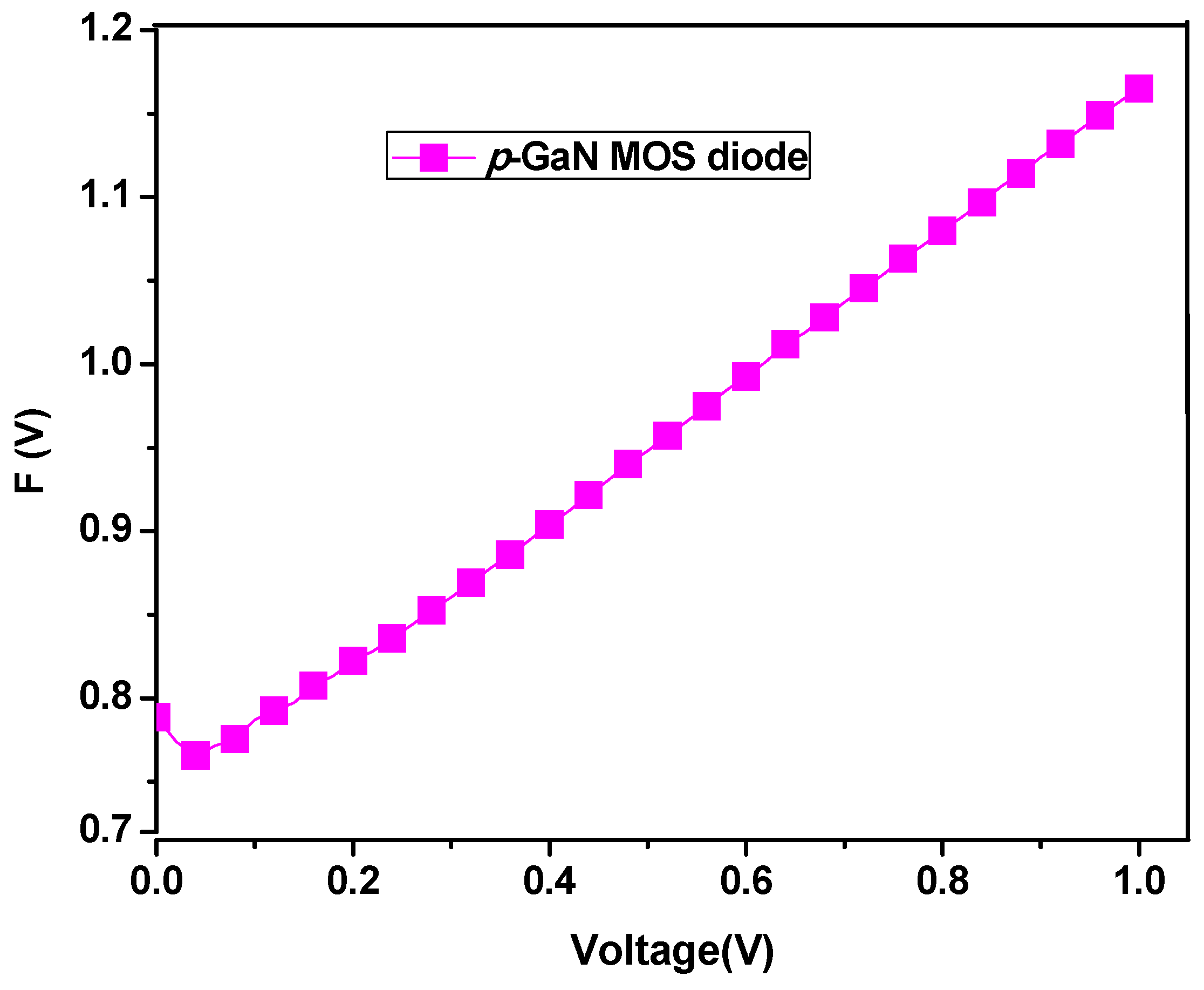
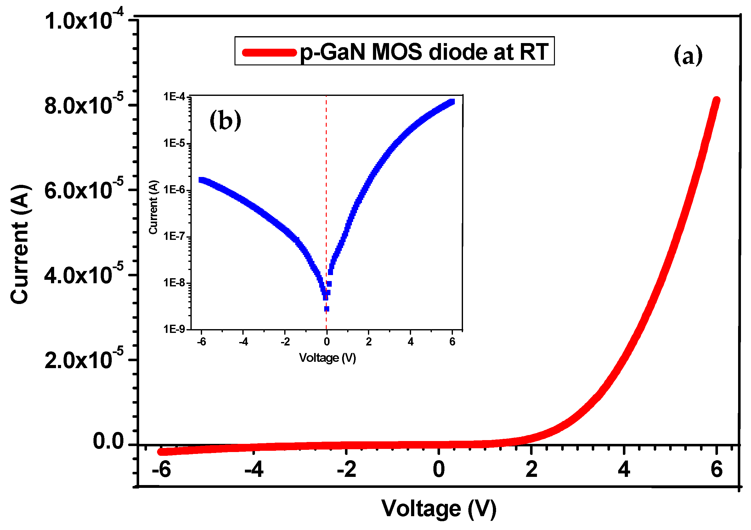
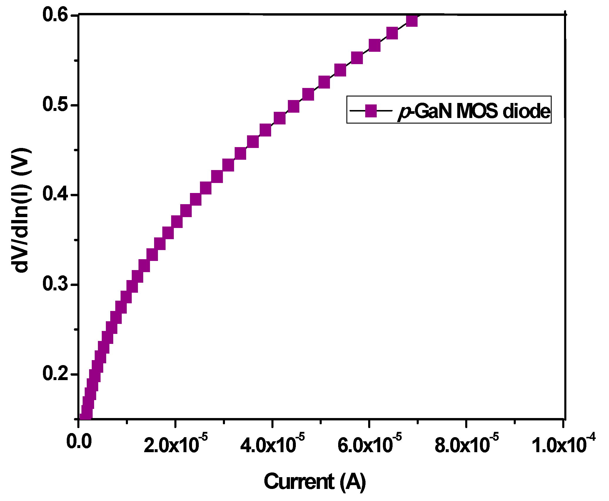
3.2. Current–Voltage (I–V) Characteristics
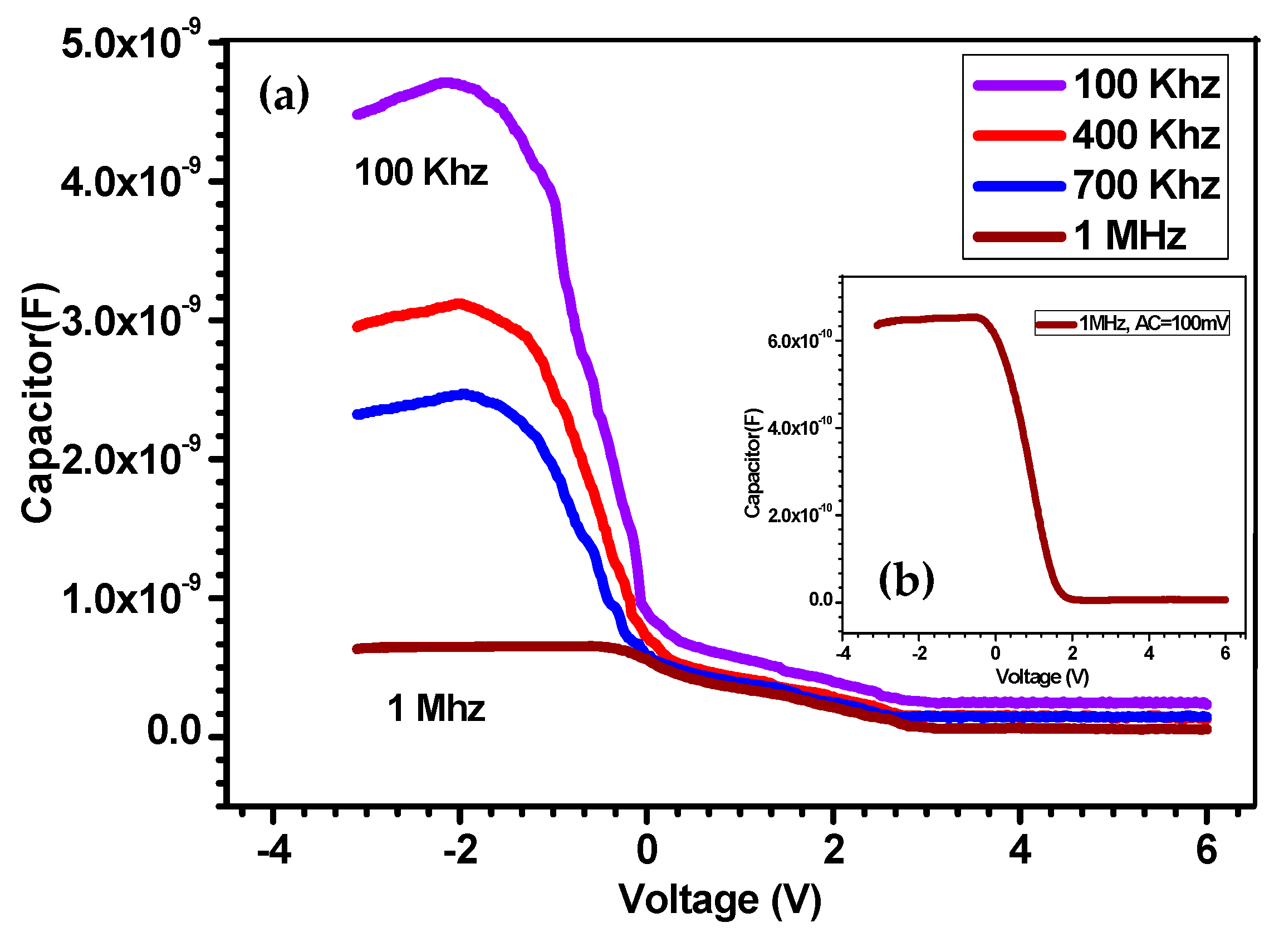
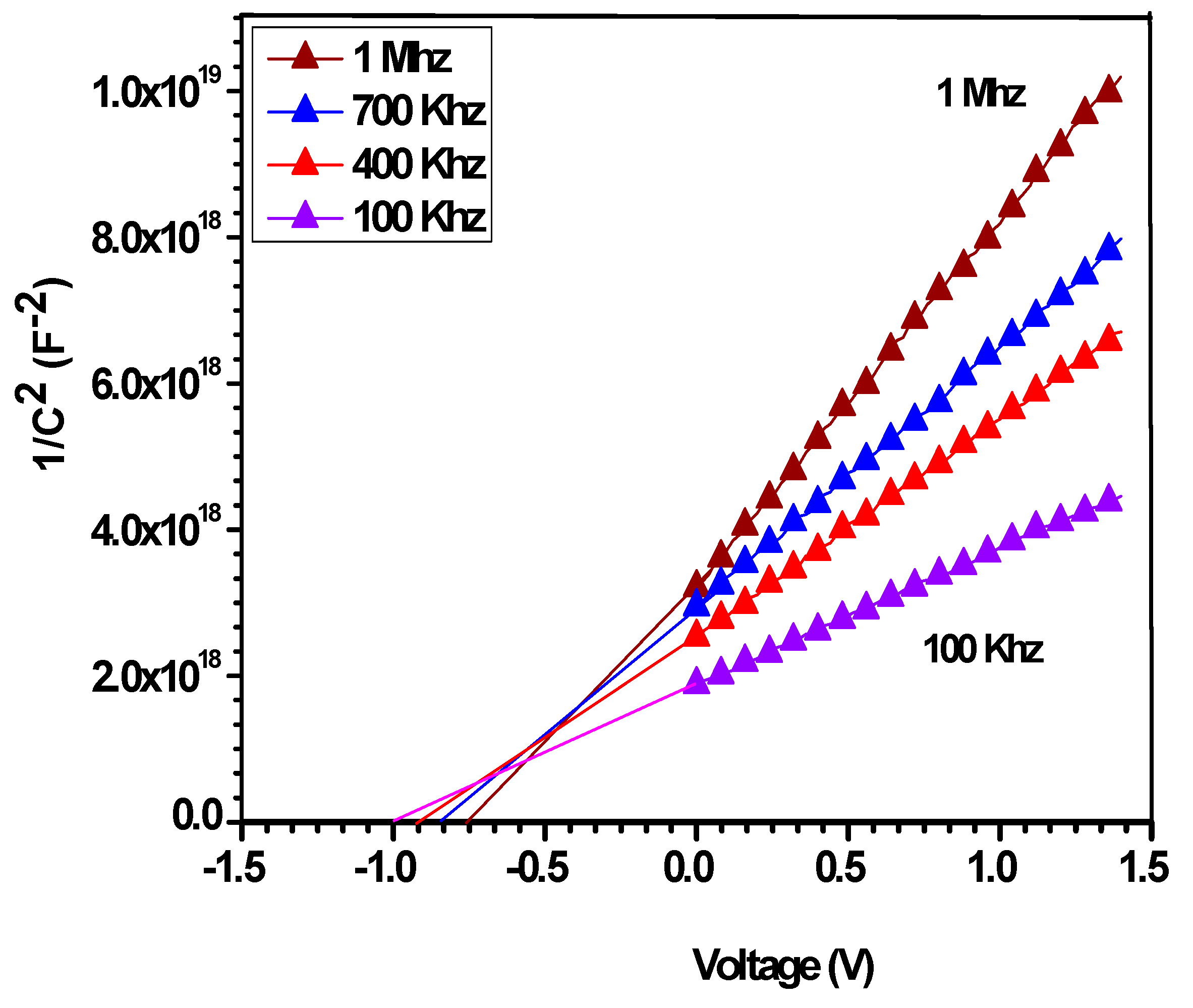
3.3. Capacitance–Voltage (C–V) Characteristics
4. Discussion
5. Conclusions
Author Contributions
Funding
Conflicts of Interest
References
- Arslan, E.; Bütüna, S.; Safak, Y.; Özbaya, E.; Uslu, H. Electrical characterization of MS and MIS structures on AlGaN/AlN/GaN heterostructures. Microelectron. Reliab. 2011, 51, 370–375. [Google Scholar] [CrossRef]
- Chang, P.C.; Yu, C.L.; Chiu, Y.J.; Liu, C.H.; Chang, S.J.; Su, Y.K.; Chuang, R.W. Ir/Pt Schottky contact oxidation for nitride-based Schottky barrier diodes. Phys. Status Solidi C 2007, 5, 1625–1628. [Google Scholar] [CrossRef]
- Li, C.C.; Kuo, D.H. Effects of growth temperature on electrical and structural properties of sputtered GaN films with a cermet target. J. Mater. Sci. Mater. Electron. 2014, 25, 1404–1409. [Google Scholar] [CrossRef]
- Reddy, M.S.; Reddy, V.R.; Choi, C.J. Electrical properties and interfacial reactions of rapidly annealed Ni/Ru Schottky rectifiers on n-type GaN. J. Alloys. Comp. 2010, 503, 186–191. [Google Scholar] [CrossRef]
- Reddy, R.; Rao, P.K. ;Annealing temperature effect on electrical and structural properties of Cu/Au Schottky contacts to n-type GaN. Microelectron. Eng. 2008, 85, 470–476. [Google Scholar] [CrossRef]
- Tuan, T.T.A.; Kuo, D.H.; Li, C.C.; Yen, W.C. Schottky barrier characteristics of Pt contacts to all sputtering-made n-type GaN and MOS diodes. J. Mater. Sci. Mater. Electron. 2014, 25, 3264–3270. [Google Scholar] [CrossRef]
- Bengi, S.; Bülbül, M.M. Electrical and dielectric properties of Al/HfO2/p-Si MOS device at high temperatures. Curr. Appl. Phys. 2013, 25, 1819–1825. [Google Scholar] [CrossRef]
- Tsevas, S.; Vasilopoulou, M.; Kouvatsos, D.N.; Speliotis, T.; Niarchos, D. Characteristics of MOS diodes fabricated using sputter-deposited W or Cu/W film. Microelectron. Eng. 2006, 83, 1434–1437. [Google Scholar] [CrossRef]
- Reddy, V.R.; Reddy, M.S.; Lakshmi, B.P.; Kumar, A. Electrical characterization of Au/n-GaN metal-semiconductor and Au/SiO2/n-GaN metal-insulator-semiconductor structures. J. Alloys. Comp. 2011, 509, 8001–8007. [Google Scholar] [CrossRef]
- Lin, K.W.; Chen, H.; Cheng, C.C.; Chuang, H.-M.; Lu, C.T.; Liu, W.C. Characteristics of a new Pt/oxide/In0.49Ga0.51P hydrogen-sensing Schottky diode. Sens. Act. B 2003, 94, 145–151. [Google Scholar] [CrossRef]
- Tuan, T.T.A.; Kuo, D.H. Characteristics of RF reactive sputter-deposited Pt/SiO2/n-InGaN MOS Schottky diodes. Mater. Sci. Semicond. Process. 2015, 30, 314–320. [Google Scholar] [CrossRef]
- Liu, I.P.; Chang, C.H.; Huang, J.; Lin, K.W. Hydrogen sensing characteristics of a Pd/Nickel oxide/GaN-based Schottky diode. Int. J. Hydrogen Energy 2019, 44, 5748–5754. [Google Scholar] [CrossRef]
- Lakshmi, B.P.; Reddy, M.S.; Kumar, A.A.; Reddy, V.R. Electrical transport properties of Au/SiO2/n-GaN MIS structure in a wide temperature range. Curr. Appl. Phys. 2012, 12, 765–772. [Google Scholar] [CrossRef]
- Juang, F.R.; Fang, Y.K.; Chiu, H.Y. Dependence of the Au/SnOx/n-LTPS/glass thin film MOS Schottky diode CO gas sensing performances on operating temperature. Microelectron. Reliab. 2012, 32, 160–165. [Google Scholar] [CrossRef]
- Tsai, T.H.; Huang, J.R.; Lin, K.W.; Hsu, W.C.; Chen, H.I.; Liu, W.C. Improved hydrogen sensing characteristics of a Pt/SiO2/GaN Schottky diode. Sens. Act. B 2008, 129, 292–302. [Google Scholar] [CrossRef]
- Cheng, C.C.; Tsai, Y.Y.; Lin, K.W.; Chen, H.I.; Lu, C.T.; Liu, W.C. Hydrogen sensing characteristics of a Pt-oxide-Al0.3Ga0.7As MOS Schottky diode. Sens. Act. B 2004, 99, 292–302. [Google Scholar] [CrossRef]
- Chen, H.I.; Chang, C.C.; Lu, H.H.; Liu, I.-P.; Chen, W.C.; Ke, B.Y.; Liu, W.C. Hydrogen sensing performance of a Pd/HfO2/GaN metal-oxide-semiconductor (MOS) Schottky diode. Sens. Act B 2018, 262, 852–859. [Google Scholar] [CrossRef]
- Karadeniz, S.; Tuğluoğlu, N.; Serin, T. Substrate temperature dependence of series resistance in Al/SnO2/p-Si (111) Schottky diodes prepared by spray deposition method. Appl. Surf. Sci. 2004, 233, 5–13. [Google Scholar] [CrossRef]
- Chang, C.F.; STai, T.H.; Chen, H.I.; Lin, K.W.; Chen, T.P.; Chen, L.Y.; Liu, Y.C.; Liu, W.C. Hydrogen sensing properties of a Pd/SiO2/AlGaN-based MOS diode. Electrochem. Communi. 2009, 11, 65–67. [Google Scholar] [CrossRef]
- Li, C.C.; Kuo, D.H. Material and technology developments of the totally sputtering-made p-n GaN diodes for cost-effective power electronics. J. Mater. Sci. Mater. Electron. 2014, 25, 1942–1948. [Google Scholar] [CrossRef]
- Tuan, T.T.A.; Kuo, D.H.; Li, C.C.; Li, G.Z. Effect of temperature dependence on electrical characterization of p-n GaN diode fabricated by RF magnetron sputtering. Mater. Sci. Appl. 2015, 6, 809–817. [Google Scholar]
- Ramesh, C.K.; Reddy, V.R.; Choi, C.J. Electrical characteristics of molybdenum Schottky contacts on n-type GaN. Mater. Sci. Eng. B 2004, 112, 30–33. [Google Scholar] [CrossRef]
- Barış, B. Analysis of device parameters for Au/TiO2/n-Si (100) metal-oxide semiconductor (MOS) diodes. Phys. B 2014, 438, 65–69. [Google Scholar] [CrossRef]
- Cheung, S.K.; Cheung, N.W. Extraction of Schottky diode parameters from forward current-voltage characteristics. Appl. Phys. Lett. 1986, 49, 85–87. [Google Scholar] [CrossRef]
- Tuan, T.T.A.; Kuo, D.H.; Saragih, A.D.; Li, G.Z. Electrical properties of RF-sputtered Zn-doped GaN films and p-Zn-GaN/n-Si hetero junction diode with low leakage current of 109A and a high rectification ratio above 105. Mater. Sci. Eng. B 2017, 222, 18–25. [Google Scholar] [CrossRef]
- Ravinandan, M.; Rao, P.K.; Reddy, V.R. Temperature dependence of current-voltage I–V characteristics of Pt/Au Schottky contacts on n-type GaN. J. Optoelectron. Adv. Mater. 2008, 10, 2787–2792. [Google Scholar]
- Norde, H. A modified forward IV plot for Schottky diodes with high series resistance. J. Appl. Phys. 1979, 50, 5052–5053. [Google Scholar] [CrossRef]
- Tuan, T.T.A.; Kuo, D.H. Temperature-dependent electrical propertiesof the sputtering-made n-InGaN/p-GaN junction diode with a breakdown voltage above 20 V. Mater. Sci. Semicond. Process. 2015, 32, 160–165. [Google Scholar] [CrossRef]


| Sample | Leakage Current (A) at −1 (V) | Schottky Barrier Height (SBH) (eV) | From I–V | Cheungs’ Function dV/dln(I)–I | ||
|---|---|---|---|---|---|---|
| I–V | Norde | n | Rs (Ω) | n | ||
| As-dep. | 4.49 × 10⁻⁸ | 0.67 | 0.78 | 3.32 | 5914 | 3.51 |
| Frequency (KHz) | Np (cm−3) | EF (eV) | V0 (eV) | ||
|---|---|---|---|---|---|
| 1000 | 3.92 × 10¹⁶ | 0.109 | 0.75 | 0.039 | 0.88 |
| 700 | 4.20 × 10¹⁶ | 0.106 | 0.82 | 0.042 | 0.94 |
| 400 | 4.89 × 10¹⁶ | 0.103 | 0.90 | 0.044 | 1.02 |
| 100 | 5.36 × 10¹⁶ | 0.099 | 0.99 | 0.046 | 1.06 |
© 2019 by the authors. Licensee MDPI, Basel, Switzerland. This article is an open access article distributed under the terms and conditions of the Creative Commons Attribution (CC BY) license (http://creativecommons.org/licenses/by/4.0/).
Share and Cite
Thi, T.A.T.; Kuo, D.-H.; Cao, P.T.; Quoc-Phong, P.; Nghi, V.K.; Tran, N.P.L. Electrical and Structural Properties of All-Sputtered Al/SiO2/p-GaN MOS Schottky Diode. Coatings 2019, 9, 685. https://doi.org/10.3390/coatings9100685
Thi TAT, Kuo D-H, Cao PT, Quoc-Phong P, Nghi VK, Tran NPL. Electrical and Structural Properties of All-Sputtered Al/SiO2/p-GaN MOS Schottky Diode. Coatings. 2019; 9(10):685. https://doi.org/10.3390/coatings9100685
Chicago/Turabian StyleThi, Tran Anh Tuan, Dong-Hau Kuo, Phuong Thao Cao, Pham Quoc-Phong, Vinh Khanh Nghi, and Nguyen Phuong Lan Tran. 2019. "Electrical and Structural Properties of All-Sputtered Al/SiO2/p-GaN MOS Schottky Diode" Coatings 9, no. 10: 685. https://doi.org/10.3390/coatings9100685
APA StyleThi, T. A. T., Kuo, D.-H., Cao, P. T., Quoc-Phong, P., Nghi, V. K., & Tran, N. P. L. (2019). Electrical and Structural Properties of All-Sputtered Al/SiO2/p-GaN MOS Schottky Diode. Coatings, 9(10), 685. https://doi.org/10.3390/coatings9100685