The Effect of RF Sputtering Conditions on the Physical Characteristics of Deposited GeGaN Thin Film

 , ,
, ,
Abstract
:
1. Introduction
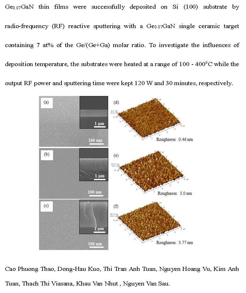
2. Experimental Details
3. Results and Discussion
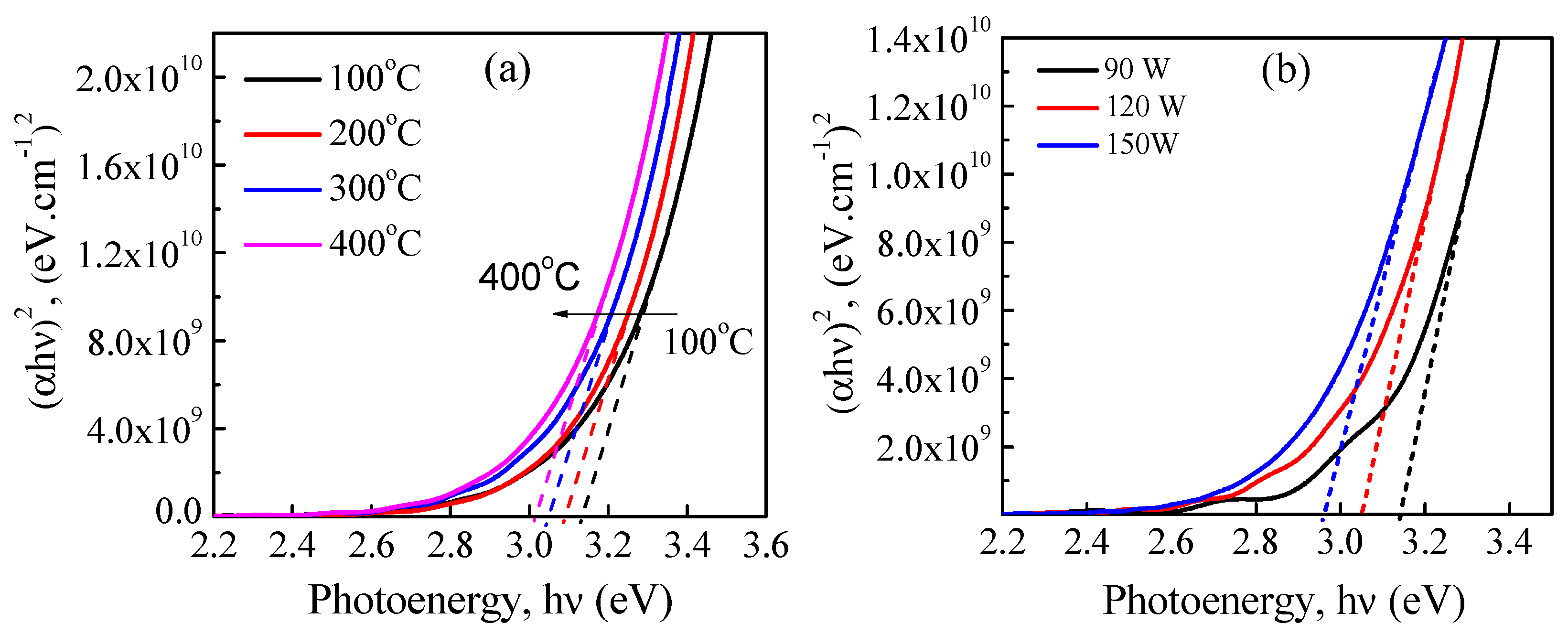
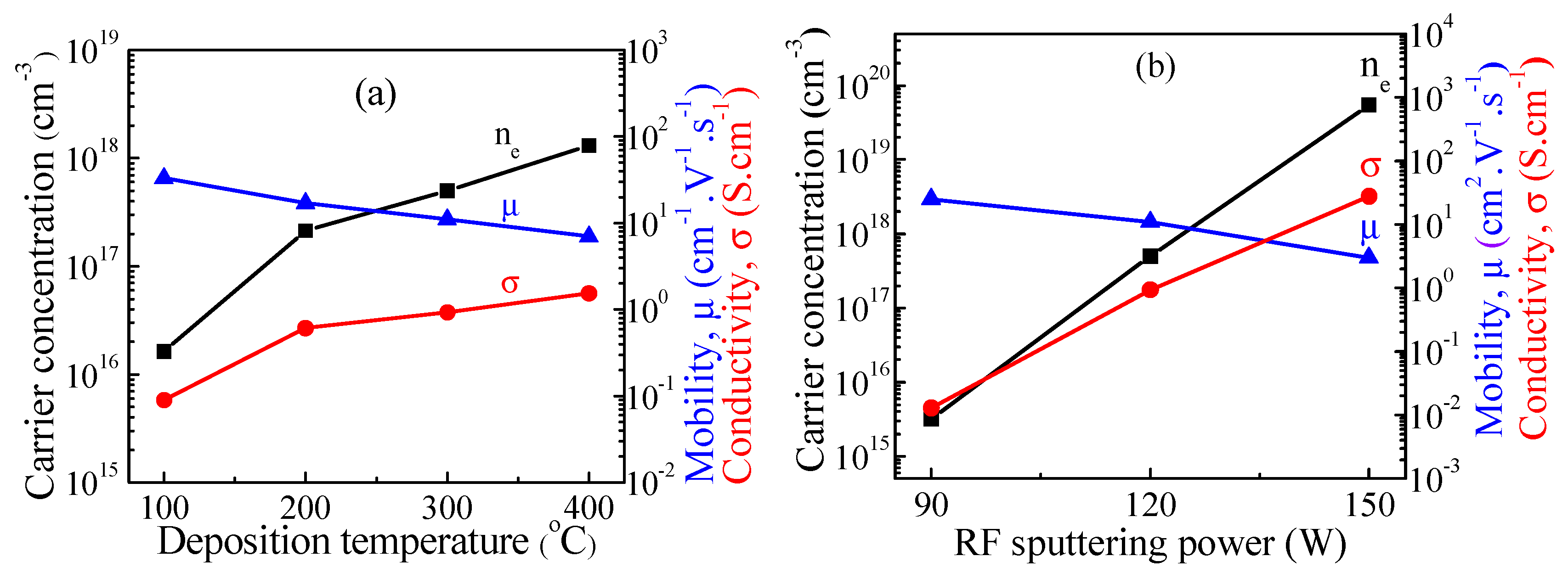
3.1. Effects of Growth Temperature on the Sputtered GeGaN Film Properties
3.2. Influences of RF Sputtering Power on the Electrical, Optical and Structural Properties of Ge-Doped Gan Thin Films
4. Conclusions
Author Contributions
Funding
Conflicts of Interest
References
- Akasaki, I.; Amano, H. Crystal growth and conductivity control of group III nitride semiconductors and their application to short wavelength light emitters. Jpn. J. Appl. Phys. 1997, 36, 5393–5408. [Google Scholar] [CrossRef]
- Fujii, T.; Gao, Y.; Sharma, R.; Hu, E.L.; DenBaars, S.P.; Nakamura, S. Increase in the extraction efficiency of GaN-based light-emitting diodes via surface roughening. Appl. Phys. Lett. 2004, 84, 855–857. [Google Scholar] [CrossRef]
- Pearton, S.J.; Ren, F.; Zhang, A.P.; Lee, K.P. Fabrication and performance of GaN electronic devices. Mater. Sci. Eng. R Rep. 2000, 30, 205–212. [Google Scholar] [CrossRef]
- Tuan, T.T.A.; Kuo, D.-H. Characteristics of RF reactive sputter-deposited Pt/SiO2/n-InGaN MoS Schottky diodes. Mater. Sci. Semicond. Process. 2015, 30, 314–320. [Google Scholar] [CrossRef]
- Tuan, T.T.A.; Kuo, D.-H.; Saragih, A.D.; Li, G.-Z. Electrical properties of RF-sputtered Zn-doped GaN films and p-Zn-GaN/n-Si hetero junction diode with low leakage current of 10−9A and a high rectification ratio above 105. Mater. Sci. Eng. B. 2017, 222, 18–25. [Google Scholar] [CrossRef]
- Kuo, D.-H.; Liu, Y.-T. Characterization of quaternary Zn/Sn-codoped GaN films obtained with ZnxSn0.04GaN targets at different Zn contents by the RF reactive magnetron sputtering technology. J. Mater. Sci. 2018, 53, 9099–9106. [Google Scholar] [CrossRef]
- Nakamura, S.; Mukai, T.; Senoh, M. Si- and Ge-doped GaN films grown with GaN buffer layers. Jpn. J. Appl. Phys. 1992, 31, 2883–2888. [Google Scholar] [CrossRef]
- Hageman, P.R.; Schaff, W.J.; Janinski, J.; Liliental-Weber, Z. n-type doping of wurtzite GaN with germanium grown with plasma-assisted molecular beam epitaxy. J. Cryst. Growth. 2004, 267, 123–128. [Google Scholar] [CrossRef]
- Colussi, M.L.; Baierle, R.J.; Miwa, R.H. Doping effects of C, Si and Ge in wurtzite [0001] GaN, AlN, and InN nanowires. J. Appl. Phys. 2011, 110, 033709. [Google Scholar] [CrossRef]
- Oshima, Y.; Yoshida, T.; Watanabe, K.; Mishima, T. Properties of Ge-doped, high-quality bulk GaN crystals fabricated by hydride vapor phase epitaxy. J. Cryst. Growth. 2010, 312, 3569–3573. [Google Scholar] [CrossRef]
- Kirste, R.; Hoffmann, M.P.; Sachet, E.; Bobea, M.; Bryan, Z.; Bryan, I.; Nenstiel, C.; Hoffmann, A.; Maria, J.-P.; Collazo, R.; et al. Ge doped GaN with controllable high carrier concentration for plasmonic applications. Appl. Phys. Lett. 2013, 103, 242107. [Google Scholar] [CrossRef]
- Shikanaia, A.; Fukahori, H.; Kawakami, Y.; Hazu, K.; Sota, T.; Mitani, T.; Mukai, T.; Fujita, S. Optical properties of Si-, Ge- and Sn-doped GaN. Phys. Status. Solidi. B 2003, 235, 26–30. [Google Scholar] [CrossRef]
- Dadgar, A.; Bläsing, J.; Diez, A.; Krost, A. Crack-free, highly conducting GaN layers on Si substrates by Ge doping. Appl. Phys. Express. 2011, 4, 011001. [Google Scholar] [CrossRef]
- Fritze, S.; Dadgar, A.; Witte, H.; Bügler, M.; Rohrbeck, A.; Bläsing, J.; Hoffmann, A.; Krost, A. High Si and Ge n-type doping of GaN doping-Limits and impact on stress. Appl. Phys. Lett. 2012, 100, 122104. [Google Scholar] [CrossRef]
- Özen, S.; Korkmaz, Ş.; Şenay, V.; Pat, S. The substrate effect on Ge doped GaN thin films coated by thermionic vacuum arc. J. Mater. Sci.: Mater. Electron. 2017, 28, 1288–1293. [Google Scholar] [CrossRef]
- Thao, C.P.; Kuo, D.H. Electrical and structural characteristics of Ge-doped GaN thin films and its hetero-junction diode made all by RF reactive sputtering. Mater. Sci. Semicond Process 2018, 74, 336–341. [Google Scholar] [CrossRef]
- Li, C.-C.; Kuo, D.-H. Effects of growth temperature on electrical and structural properties of sputtered GaN films with a cermet target. J. Mater. Sci.: Mater. Electron. 2014, 25, 1404–1409. [Google Scholar] [CrossRef]
- Thao, C.P.; Kuo, D.-H.; Jan, D.-J. Codoping effects of the Zn acceptor on the structural characteristics and electrical properties of the Ge donor-doped GaN thin films and its hetero-junction diodes all made by reactive sputtering. Mater. Sci. Semicond. Process. 2018, 82, 126–134. [Google Scholar] [CrossRef]
- Li, C.-C.; Kuo, D.-H. Material and technology developments of the totally sputtering-made p/n GaN diodes for cost-effective power electronics. J. Mater. Sci.: Mater. Electron. 2014, 25, 1942–1948. [Google Scholar] [CrossRef]
- Tuan, T.T.A.; Kuo, D.-H.; Li, C.C.; Yen, W.-C. Schottky barrier characteristics of Pt contacts to all sputtering-made n-type GaN and MoS diodes. J. Mater. Sci.: Mater. Electron. 2014, 25, 3264–3270. [Google Scholar] [CrossRef]
- Ting, C.-W.; Thao, C.P.; Kuo, D.-H. Electrical and structural characteristics of tin-doped GaN thin films and its hetero-junction diode made all by RF reactive sputtering. Mater. Sci. Semicond Process. 2017, 59, 50–55. [Google Scholar] [CrossRef]
- Kim, H.W.; Kim, N.H. Preparation of GaN films on Zno buffer layers by rf magnetron sputtering. Appl. Surf. Sci. 2004, 236, 192–197. [Google Scholar] [CrossRef]
- Chyr, I.; Lee, B.; Chao, L.C.; Steckl, A.J. Damage generation and removal in the Ga+ focused ion beam micromachining of GaN for photonic applications. J. Vac. Sci. Technol. 1999, 17, 3063–3067. [Google Scholar] [CrossRef]

| Sputtering Conditions | Ga (at.%) | Ge (at.%) | N (at.%) | [Ge]/([Ga]+[Ge]) | [N]/([Ga]+[Ge]) | |
|---|---|---|---|---|---|---|
| Heating Substrate (°C) | 100 | 47.42 | 2.87 | 49.71 | 0.057 | 0.988 |
| 200 | 47.08 | 3.78 | 49.14 | 0.074 | 0.966 | |
| 300 | 46.83 | 4.35 | 48.82 | 0.085 | 0.954 | |
| 400 | 46.73 | 4.87 | 48.40 | 0.094 | 0.938 | |
| RF Sputtering Power (W) | 90 | 49.39 | 3.89 | 46.72 | 0.073 | 0.877 |
| 120 | 46.83 | 4.35 | 48.82 | 0.085 | 0.954 | |
| 150 | 47.16 | 5.19 | 47.65 | 0.099 | 0.910 | |
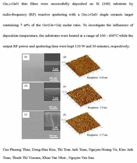
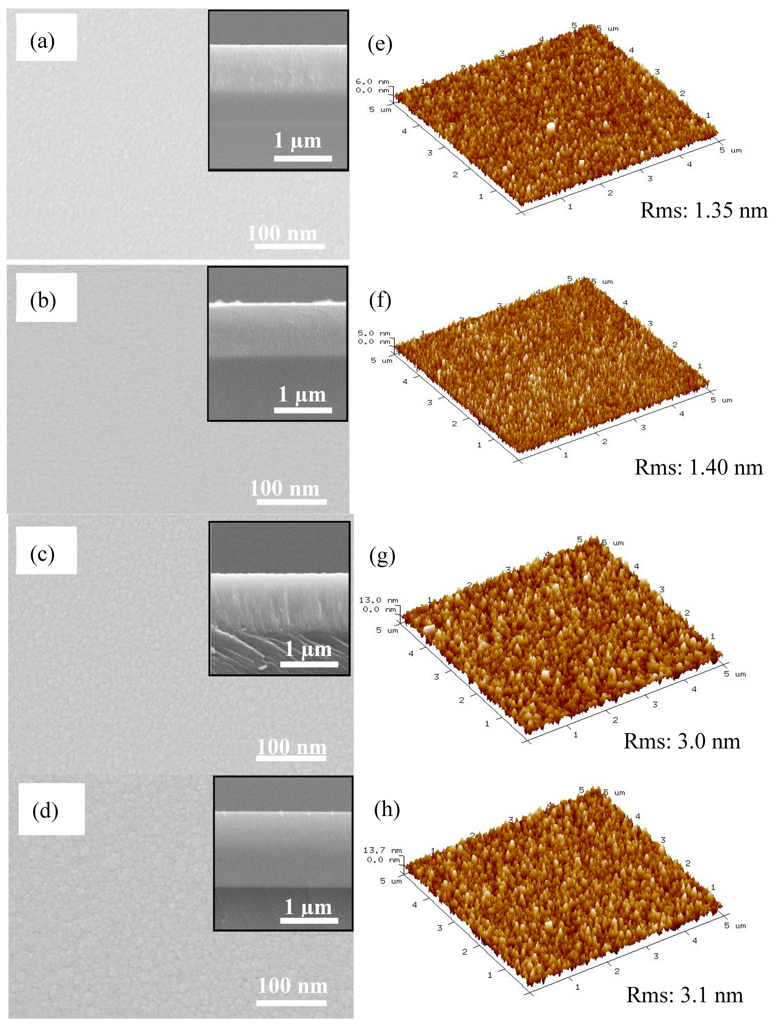
| Sputtering Conditions | Film Thickness (µm) | Deposition Rate (nm/minute) | Roughness (nm) | |
|---|---|---|---|---|
| Deposition Temperature (°C) | 100 | 1.00 | 33.33 | 1.35 |
| 200 | 1.17 | 39.00 | 1.40 | |
| 300 | 1.30 | 43.33 | 3.00 | |
| 400 | 1.78 | 59.33 | 3.10 | |
| Sputtering Power (W) | 90 | 0.62 | 20.67 | 0.46 |
| 120 | 1.30 | 43.33 | 3.00 | |
| 150 | 2.50 | 83.33 | 3.77 | |
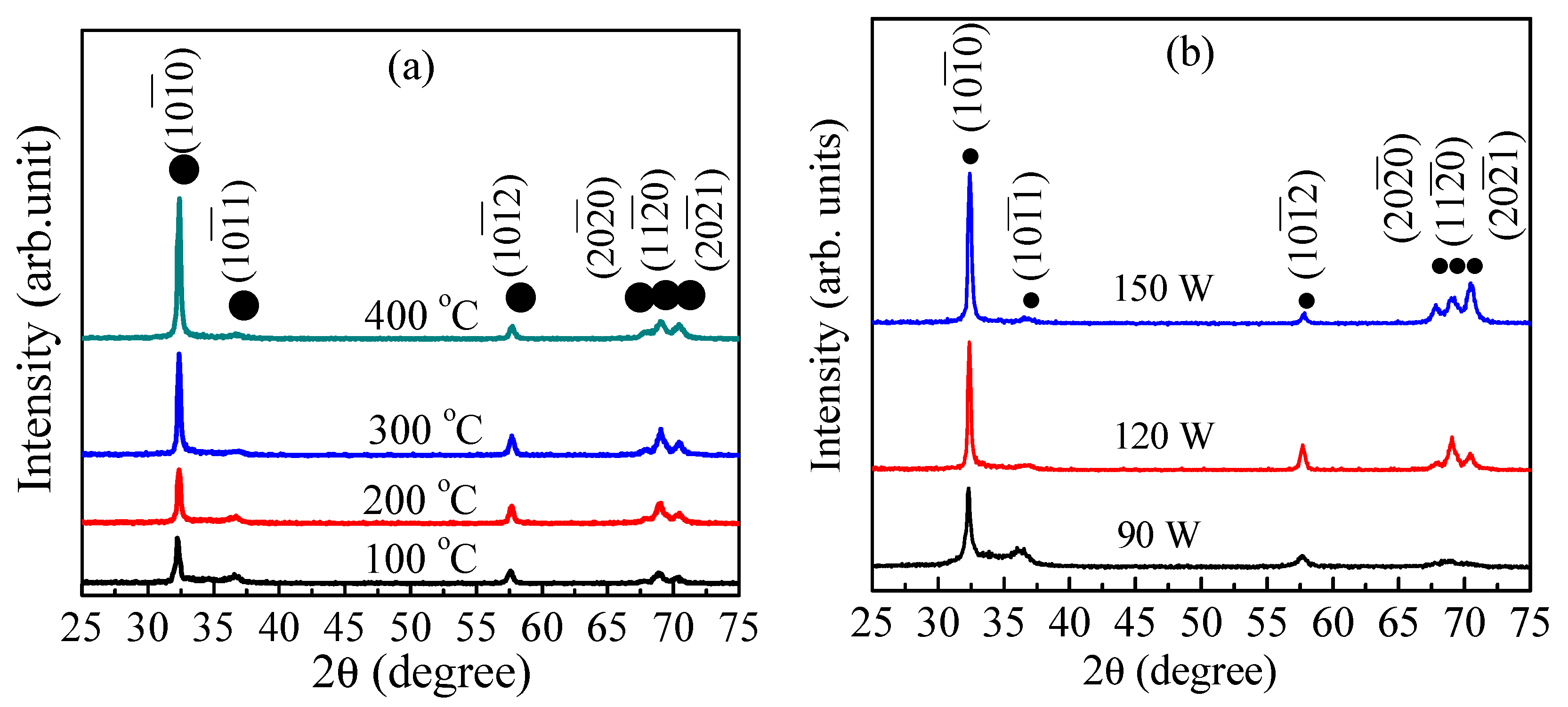
| Sputtering Conditions | 2θ peak | a (Å) | c (Å) | Volume (Å3) | FWHM () (degree) | Crystallite Size (nm) | |
|---|---|---|---|---|---|---|---|
| Deposition Temperature (°C) | 100 | 32.25 | 3.21 | 5.21 | 46.57 | 0.34 | 24.33 |
| 200 | 32.30 | 3.20 | 5.20 | 46.13 | 0.30 | 27.57 | |
| 300 | 32.36 | 3.19 | 5.18 | 45.70 | 0.27 | 30.64 | |
| 400 | 32.40 | 3.18 | 5.17 | 45.27 | 0.25 | 33.09 | |
| RF Sputtering Power (W) | 90 | 32.30 | 3.59 | 5.83 | 64.87 | 0.41 | 21.44 |
| 120 | 32.36 | 3.38 | 5.49 | 54.26 | 0.27 | 33.04 | |
| 150 | 32.40 | 3.25 | 5.29 | 48.43 | 0.26 | 34.67 | |
| Sputtering Conditions. | Type | Concentration Ne cm−3 | Mobility μ cm2·V−1·s−1 | Conductivity σ S·cm−1 | Bandgap eV | |
|---|---|---|---|---|---|---|
| Deposition Temperature (°C) | 100 | n | 1.64 × 10¹⁶ | 33 | 0.09 | 3.14 |
| 200 | n | 2.14 × 10¹⁷ | 17 | 0.58 | 3.09 | |
| 300 | n | 5.02 × 10¹⁷ | 11 | 0.88 | 3.05 | |
| 400 | n | 1.30 × 10¹⁸ | 7 | 1.46 | 3.02 | |
| Sputtering Power (W) | 90 | n | 3.22 × 10¹⁵ | 25 | 0.012 | 3.14 |
| 120 | n | 5.02 × 10¹⁷ | 11 | 0.84 | 3.05 | |
| 150 | n | 5.50 × 10¹⁹ | 4 | 35.2 | 2.96 | |
© 2019 by the authors. Licensee MDPI, Basel, Switzerland. This article is an open access article distributed under the terms and conditions of the Creative Commons Attribution (CC BY) license (http://creativecommons.org/licenses/by/4.0/).
Share and Cite
Thao, C.P.; Kuo, D.-H.; Tuan, T.T.A.; Tuan, K.A.; Vu, N.H.; Via Sa Na, T.T.; Nhut, K.V.; Sau, N.V. The Effect of RF Sputtering Conditions on the Physical Characteristics of Deposited GeGaN Thin Film. Coatings 2019, 9, 645. https://doi.org/10.3390/coatings9100645
Thao CP, Kuo D-H, Tuan TTA, Tuan KA, Vu NH, Via Sa Na TT, Nhut KV, Sau NV. The Effect of RF Sputtering Conditions on the Physical Characteristics of Deposited GeGaN Thin Film. Coatings. 2019; 9(10):645. https://doi.org/10.3390/coatings9100645
Chicago/Turabian StyleThao, Cao Phuong, Dong-Hau Kuo, Thi Tran Anh Tuan, Kim Anh Tuan, Nguyen Hoang Vu, Thach Thi Via Sa Na, Khau Van Nhut, and Nguyen Van Sau. 2019. "The Effect of RF Sputtering Conditions on the Physical Characteristics of Deposited GeGaN Thin Film" Coatings 9, no. 10: 645. https://doi.org/10.3390/coatings9100645
APA StyleThao, C. P., Kuo, D.-H., Tuan, T. T. A., Tuan, K. A., Vu, N. H., Via Sa Na, T. T., Nhut, K. V., & Sau, N. V. (2019). The Effect of RF Sputtering Conditions on the Physical Characteristics of Deposited GeGaN Thin Film. Coatings, 9(10), 645. https://doi.org/10.3390/coatings9100645