1. Introduction
Concentrated solar power (CSP) systems generate solar power by using mirrors or lenses (primary concentrators or reflectors) to concentrate a large area of sunlight, or solar thermal energy, onto a smaller area (the receiver). A secondary concentrator reflects the sunlight coming from the primary concentrators onto the absorbing receiver. They ensure the gathering and redirecting, and in some applications further concentration and focusing, of the solar beams towards the absorber. A good overview of the available different secondary reflector material systems and different CSP configurations is given in [
1].
A secondary reflector which is installed adjacent to the solar tower or linear Fresnel collector receiver can improve the optical efficiency of the system considerably as well as reducing its cost by [
2]:
Reducing the amount of flux which is spilled-off the target
Improving the flux distribution uniformity
Decreasing heat losses and CAPEX (capital expenditure) by reducing the receiver size
The main challenge for such a mirror is its high operation temperature. For the solar power tower, the high temperatures evolve mainly due to the amount of irradiance that is being absorbed by the mirror, and to a lesser extent due to convective heat exchange with its surrounding. One possible approach is to water-cool the mirror. However, this solution will mean an investment increase, technical challenges, and cause a plant shut-down in case of any failure of the cooling system.
A different approach avoiding water-cooling was to develop a protected silver coated secondary mirror which could retain its optical and mechanical properties up to 350 °C. The developed mirrors are based on a sputtered silver layer and several adhesion and barrier layers on a highly polished steel substrate. The silver layers are sputtered using either standard direct current magnetron sputtering (DC MS) or, alternatively, high-power impulse magnetron sputtering (HiPIMS) [
3]. With HiPIMS, high power (up to megawatt range) is applied to the magnetron target in unipolar pulses at a low duty cycle and low repetition frequency while keeping the average power about two orders of magnitude lower than the peak power. This results in a high plasma density and high ionization fraction of the sputtered vapor. Previous studies with silver HiPIMS layers show an improvement in electrical conductance attributed to atomically smoother and denser films [
4,
5] being grown from the high energy flux of the sputtered silver.
For protected silver coatings for reflector applications, a desired improvement in both reflectance and film stability was the motivation to investigate HiPIMS silver in comparison to the standard DC MS silver. As the silver films must be durable at high temperature, the films were examined (optically and micro-structurally) as deposited and after exposure to a temperature of 400 °C (plausible operational conditions for the stringent solar power tower reflector). It should be noted that the protected silver coatings were tested under different conditions (e.g., a humidity and heat of 85% and 85 °C, respectively), but that is not the focus of the paper here. Other applications of protected sputtered silver where highly reflective yet highly durable reflector coatings are required, include telescopes (such as the coatings used at the Gemini Observatory telescope [
6]) or in robust floodlight applications.
2. Materials and Methods
The HiPIMS and DC MS silver films were prepared in house at the Fraunhofer Insitute of Solar Energy Systems. Both processes used 99.99% pure silver targets which were sputtered in argon atmospheres of approximately 300 Pa. A TruPlasma Highpulse 4008 DC generator (Trumpf-Hüttinger, Freiburg, Germany) was used for the HiPIMS mode. The DC magnetron was powered by a TIG-DCS (Trumpf-Hüttinger, Freiburg, Germany). The electrical sputter parameters for the DC MS and HiPIMS silver are given in
Table 1. For HiPIMS deposition, a pulse frequency of 150 s
−1 and pulse duration of 80 µs was used.
A current of 12 A in the DC magnetron mode was chosen, as this was the standard silver used in the protected silver system. It exhibits the highest temperature durability for DC magnetron mode. The 200 A HiPIMS silver was deposited with a similar power density to the 12 A DC MS sample. The power density is given only as an approximate value, as it is calculated from the power and the approximate race-track area of the silver target magnetron. The measured dynamic rate, normalized to the power density, is given in
Table 1. As typically seen, HiPIMS mode led to a drop in the deposition rate for equivalent power density. This is caused by increased film density, increased self-sputtering, and sputtering of the film at higher peak currents, as discussed in [
7].
Cleaned float glass was used as a substrate for reflectance and conductivity measurements. Glass with a sputtered 45 nm NiCr (Ni:Cr 80:20 wt % target DC magnetron, 9.5 W/cm2 in an Ar pressure of 0.16 Pa) adhesion layer was used as a substrate for the reflectance, grazing incidence X-ray diffraction (GIXRD), and scanning electron microscopy (SEM) analysis. It should be noted that for the SEM and GIXRD measurements, the adhesion layer coating which the silver is sputtered on was identical for both the discrete and the protected silver.
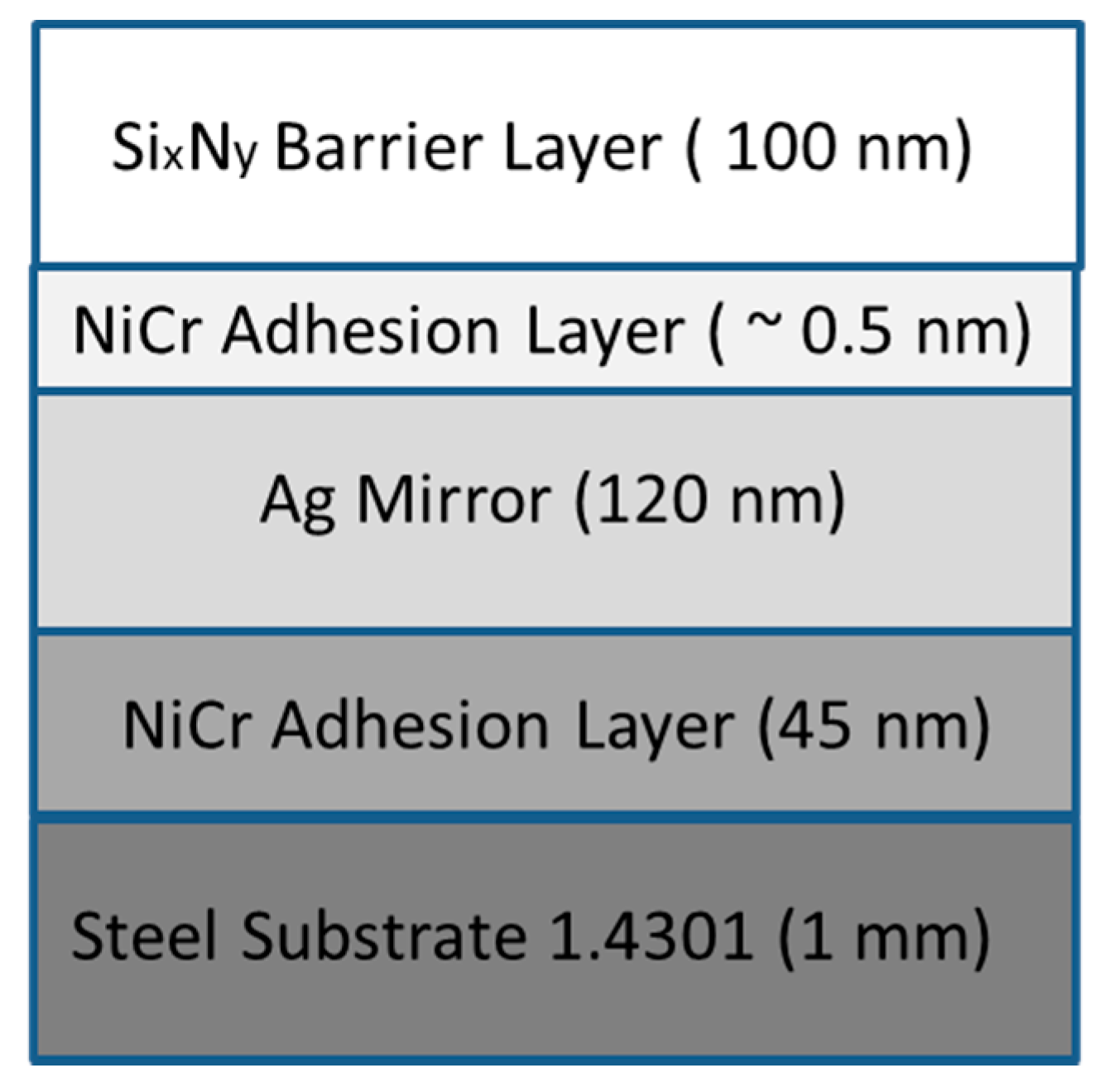
The protected silver layer system was deposited also on polished 1 mm 1.4301 steel substrates. The protected sputtered silver system was NiCr (45 nm)/Ag (120 nm)/NiCr (0.5 nm)/Si
xN
y (100 nm) and is shown in
Figure 1. The Si
xN
y barrier and NiCr adhesion layers were sputtered in sequence with the silver films. The bottom NiCr layer was as described above. The top NiCr layer used a standard DC planar magnetron (target Ni:Cr 80:20 wt %) with a power of 0.8 W/cm
2 in an Ar atmosphere of pressure 0.09 Pa. The Si
xN
y was deposited using a middle frequency, MF, dual rotary cathode (target Si:Al 90:10 wt %) at 10.8 W/cm
2 in an Ar/N2 (gas flow rate ratio 1:1) at a pressure of 0.3 Pa. The top adhesion was a nominal 0.5 nm NiCr designed to maximize the Ag-to-barrier layer adhesion with minimal reflectance degradation.
All GIXRD patterns were recorded using a Philips X’Pert MRD system equipped with a CuK
α X-ray source. The Scherrer [
8] formula,
was used as a comparative empirical guide (where
τ is the grain size;
K is a shape factor, here with a value of 0.9;
λ is the X-ray wavelength of 1.54 Å;
β is the full width half maximum; and
θ is the Bragg angle), rather than an accurate calculation of the average grain size. The shifts in peak position with annealing were estimated and compared, again to determine a trend between samples rather than a precise measurement of strain in the silver crystal lattice.
The scanning electron microscope used was a FIB-SEM Auriga 60 (Zeiss, Oberkochen, Germany). Reflectance measurements were done with a Vertex 80 spectrometer (Bruker, Ettlingen, Germany) with an integrated sphere. The solar hemispherical reflectance is the percentage of the direct and diffuse AM1.5 solar radiance reflected from the coating system. Sheet resistance measurements were taken with a four-point probe (only for pure silver-coated glass substrates). The conductivity was thus calculated from the measured film thickness. Sputtered film thickness was checked using both a Dektak 6M profilmeter (Veeco, New York, NY, USA) and a calibrated Xray Fluorescence Spectrometer, XRF, Fischerscope XDV-µ (Helmut-Fischer, Sindelfingen, Germany).
3. Results
The results section is divided into two subsections for clarity. Firstly, the results for the discrete silver films are presented, and secondly, the results for the protected silver film system are given.
3.1. Discrete Silver Films
The discrete silver thin films were investigated in addition to the protected silver film system, as having no top coatings allows for a deeper understanding of the silver layers themselves.
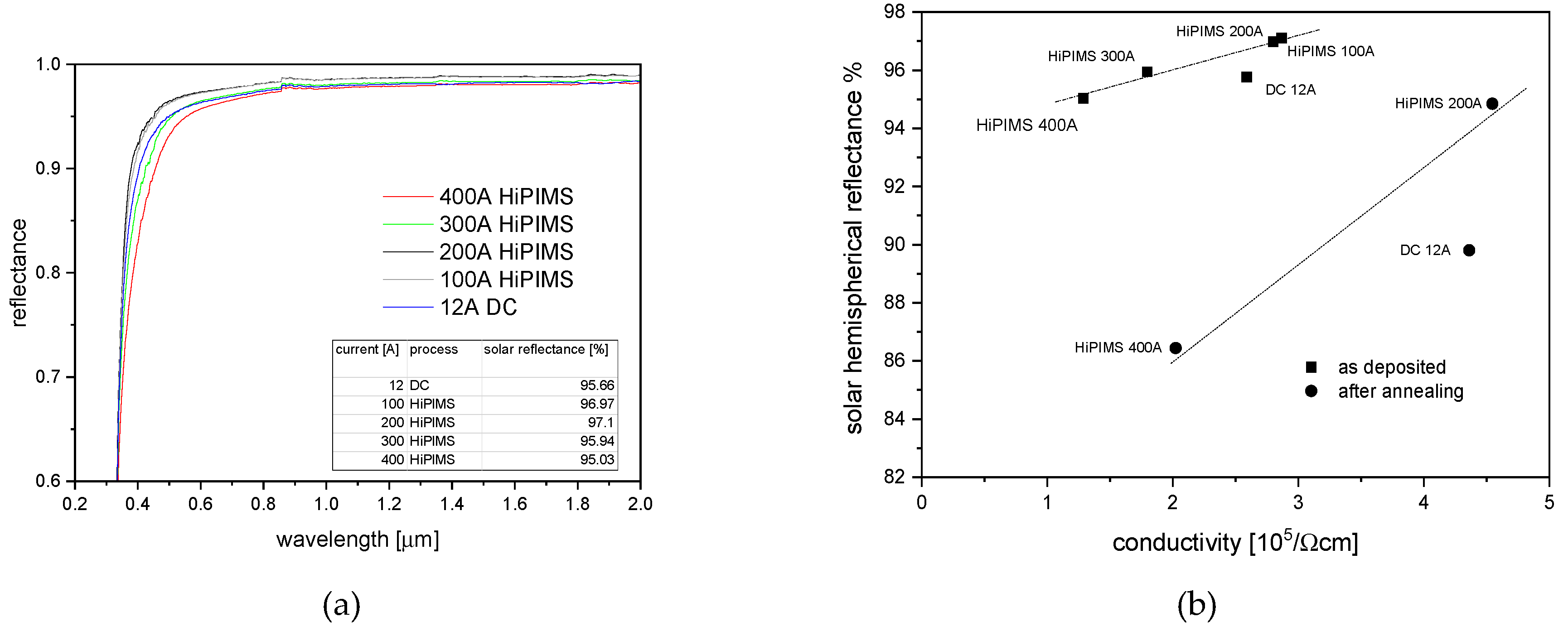
The reflectance spectra of the as-deposited discrete 500 nm silver films on glass substrates are presented in
Figure 2a. The solar reflectance increased to a maximum for the silver films deposited with 200 A in HiPIMS mode, but for higher HiPIMS currents it decreased and, indeed, with 400 A HiPIMS it was lower than the 12 A DC MS-deposited silver film. In
Figure 2b, the conductivity of the films is plotted against the global solar hemispherical reflectance. The films sputtered by HiPIMS exhibit an approximately linear relationship whereby the conductivity proportionally increases with increasing reflectance. The 12 A DC MS samples are sputtered in a different mode and exhibit a higher conductivity-to-reflectance ratio than the HiPIMS films.
The films were annealed at 400 °C for 0.5, 4, 8, 16, and 32 h, the reflectance and conductivity were subsequently measured. With increasing annealing time, the conductivity of all the silver films increased, but solar reflectance decreased. What is more, the reflectance changed from being purely specular to partially diffuse. After 8 h annealing at 400 °C, corresponding to the data shown in
Figure 2b, the 200 A HiPIMS silver films remained highly reflective (94% total) but the diffuse solar reflectance contribution was 40%, whilst the 12 A DC MS silver and the highly energetically sputtered 400 A HiPIMS silver had a lower total reflectance (89% and 84%, respectively) but also a lower diffuse contribution (10% and 2%, respectively). Due to this high optical scattering, the 200 A HiPIMS films appeared white after annealing.
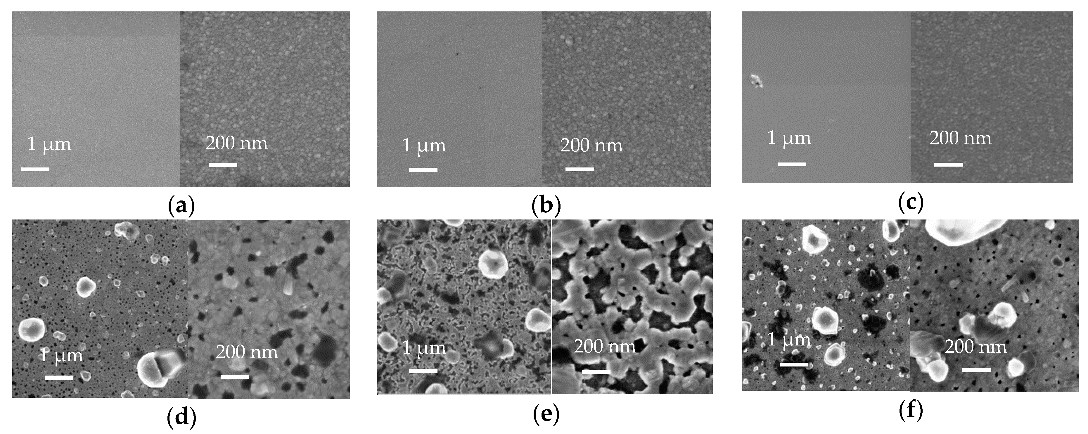
SEM pictures are shown in
Figure 3 of equivalent 120 nm silver films grown on the NiCr-coated glass. The as-deposited films appeared smooth and relatively featureless at low magnification. The grains, observable at high magnification, for the 12 A DC MS silver and the 200 A HiPIMS silver were apparently of a similar size (≤20 nm), whereas the 400 A HiPIMS grains were distinguishably smaller (≤10 nm). After annealing (again for 8 h at 400 °C), all samples exhibited the characteristic agglomeration (large crystals) and hole (void) formation of unprotected silver exposed to elevated temperatures reported in [
9]. Moreover, the grain growth in the bulk of the film was apparent for all samples. The average bulk grains, post annealing, for the 200 A HiPIMS appeared the largest (50–150 nm), whilst the 400 A HiPIMS appeared the smallest (10–50 nm).
It is clear from the SEM pictures that the smooth silver films became significantly rougher, caused by the agglomeration and voiding [
9,
10]. This can be correlated with the decrease in spectral and total solar reflectance. The rougher surface features would cause the observed pronounced scattering despite the increased grain size, with annealing, which allows the conductivity to improve, provided the film remains networked.
In
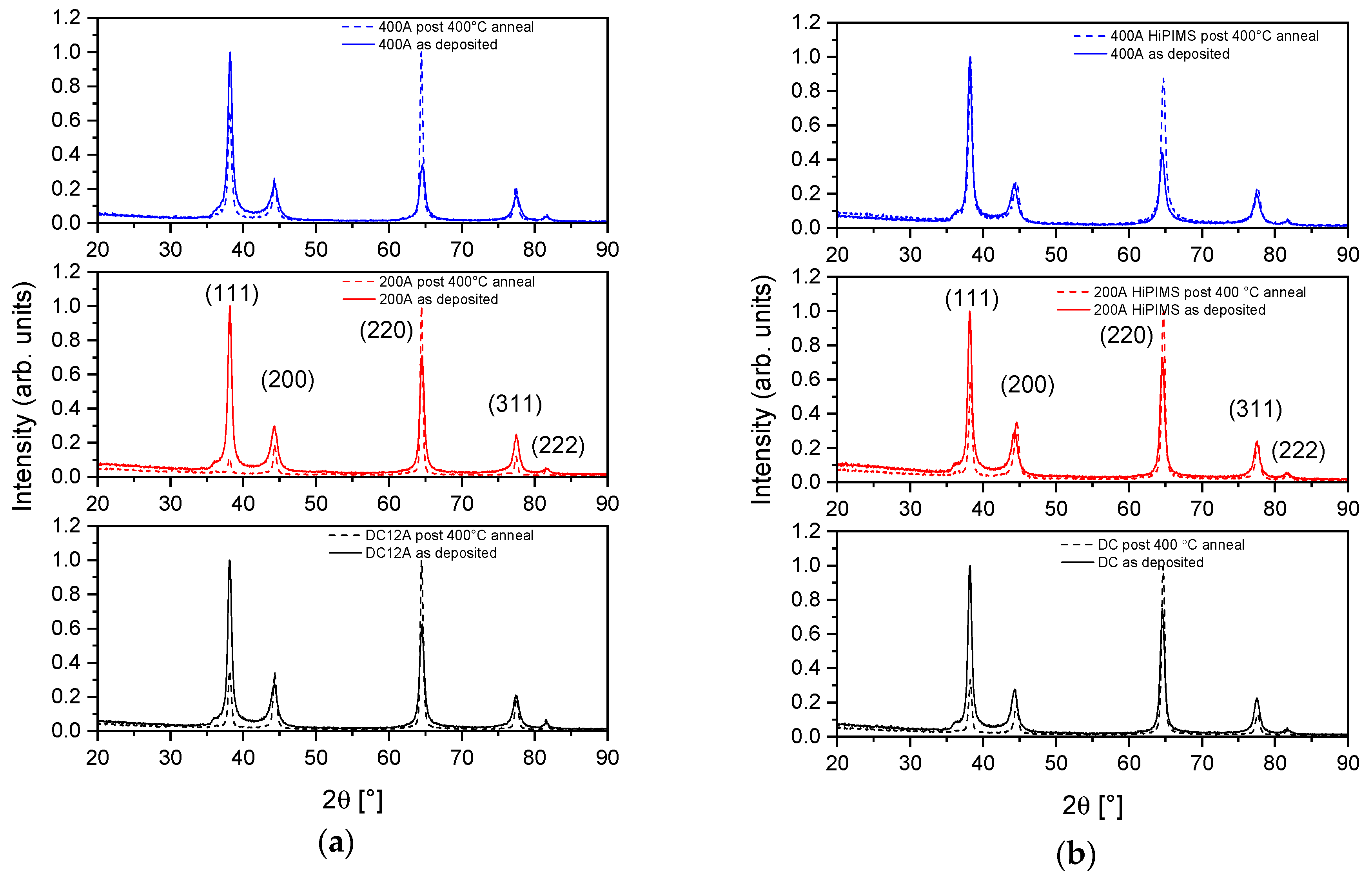
Figure 4a, the GIXRD spectra for the 400 A HiPIMS, 200 A HiPIMS, and 12 A DC MS silver films deposited on NiCr coated glass substrates, as-deposited and after an 8 h anneal at 400 °C, are shown. As stated, the grain size, peak position and intensity were calculated or measured from the spectra, and for clarity and transparency they are given in
Table S1 as supplementary material.
Randomly oriented polycrystalline silver has a diffraction peak ratio of (111):(200):(220):(311):(222) as 100:40:25:26:12 [
11]. In all as-deposited films sputtered here, the (220) plane exhibited a larger relative intensity than the random oriented reference.
After annealing, the diffraction from the (220) plane had the highest intensity, and the relative contribution from the (111) planes reduced significantly as the grains increased in orientation. This is particularly pronounced in the 200A HiPIMS silver film.
Using the Scherrer formula as a qualitative indication of grain size, it is implicated that for the as-deposited samples, the 200 A HiPIMS silver film has marginally larger grains than the 12 A DC MS silver film, but the 400 A HiPIMS silver film has grains smaller in size. This correlates with what is seen in the SEM pictures. It can be also correlated to the trend in conductivity of the silver film on the glass substrate: a smaller grain size yields lower sheet conductivity. There is no clear peak shift on annealing, although the observed narrowing of the peaks with annealing indicates grain growth in the sample, again in correlation with the SEM pictures and the increase in conductivity with annealing in equivalent films.
Figure 4b is discussed in the context of the next section.
3.2. Protected Silver Thin Film System
In this section, the results of the protected silver thin film systems will be presented.
GIXRD spectra shown in
Figure 4b for the 400 A HiPIMS, 200 A HiPIMS, and 12 A DC MS protected silver film system deposited on coated glass substrates are shown as deposited and after a 24 h anneal at 400 °C. Glass substrates were used for the GIXRD to avoid any interference diffraction peaks from the underlying steel substrate. Both the discrete silver discussed earlier and the protected silver system were grown on the same 45 nm NiCr adhesion layer coating the glass. The difference was that the protected silver system had a top NiCr adhesion and Si
xN
y barrier coating. As previously, the grain size, peak position, and intensity were calculated or measured from the spectra, and for clarity and transparency they are given in
Table S2 as supplementary material. The as-deposited protected silver films exhibit the same trend in grain sizes as the as-deposited discrete silver films, and the grains are likewise orientated. After the 24 h anneal at 400 °C, the grains were larger and became even more aligned, with the (111) peak reducing and the (220) peak increasing in amplitude. What is different from the discrete silver films is that after annealing the protected silver films, there was a clear peak shift to a higher Bragg angle. The average peak shift was higher in the HiPIMS films than in the DC MS film. This is an indication that the silver protected film is compressively strained after the annealing step.
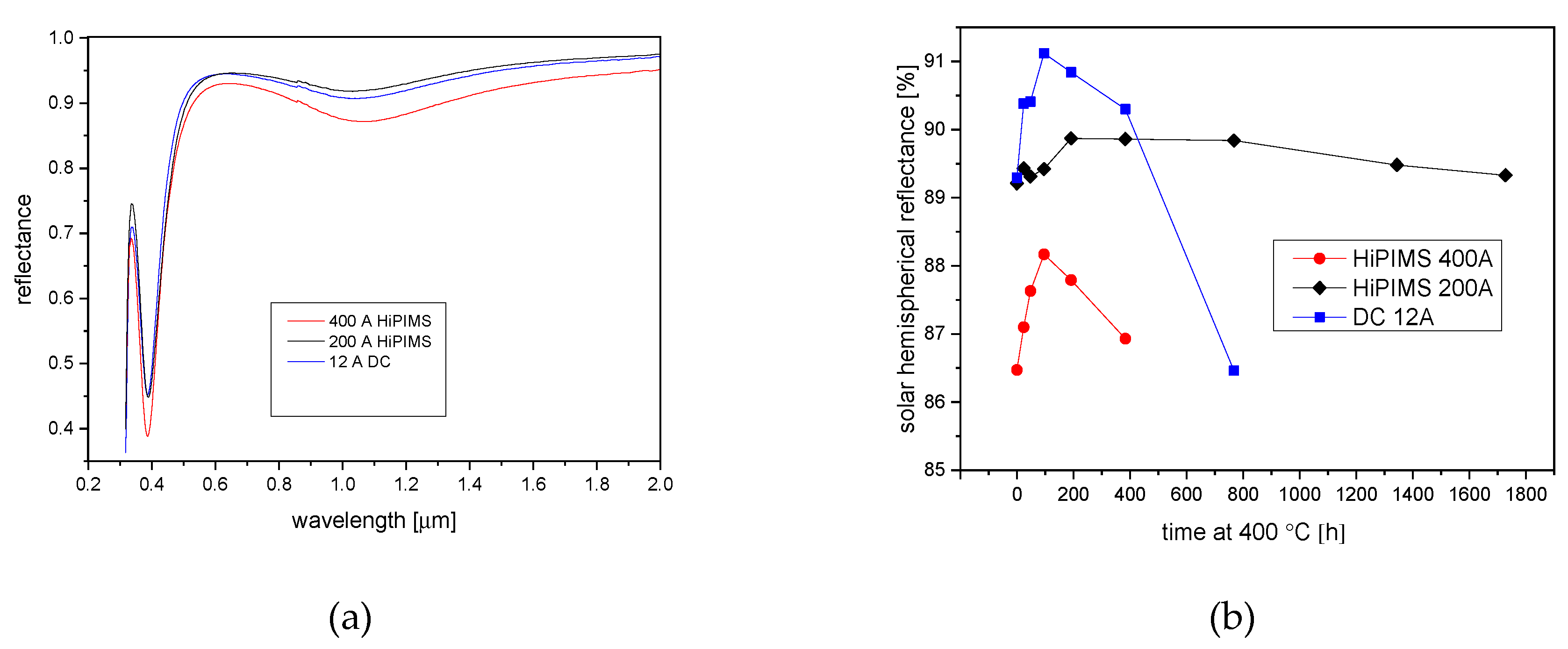
Figure 5a shows the global reflectance of the as-deposited protected silver thin films systems. The total solar reflectance of all the film systems was reduced to below 90%. In this case here, the top adhesion layer was an ultra-thin NiCr deposition (nominally 0.5 nm thick, in practice an incomplete covering). Adding additional layers, such as the Si
xN
y barrier layer, on top of the silver film reduced the total reflectance due to unwanted interference from additional interfacial reflectance and absorption by the adhesion and barrier layer. This was particularly prevalent in the UV-visible portion of the spectrum. Due to this, the gain in reflectance that was achieved for the discrete silver by depositing with the 200 A HiPIMS instead of 12 A DC MS silver was not apparent. The reflectance of the film system incorporating the 400 A HiPIMS silver was however lower, which was most likely due to the poorer silver reflectance, since the film system was identical between samples.
The protected silver thin film systems were subsequently annealed at two-fold increasing intervals, e.g., 24, 48, 96, 192, and 384 h, until the sample was deemed to have degraded, either due to degradation apparent to the eye or a loss in optical reflectance below the starting value. The silver, being embedded in the adhesion and barrier layers, was protected from corroding elements in the atmosphere as well as agglomeration. Agglomeration, which began instantaneously at 400 °C for the discrete silver films, was limited in the protected silver system by the adhesion layers and barrier layers. For the first 96 h of oven time, all the silver film systems increased in reflectance. This can be partially attributed to grain growth in the silver. This occurred in the protected silver system without surface roughening due to pronounced agglomeration, which caused the optical scattering observed in the discrete silver films. The increase in reflectance may also be due to the oxidation of the top metallic adhesion layer above the silver, which subsequently exhibited a higher transmission, particularly in the UV-visible portion of the spectrum. The increase in the 12 A DC MS and 400 HiPIMS silver film systems on annealing was a 2% absolute rise in reflectance, whereas the 200 A HiPIMS silver system increased by less than 1%.
After more than 96 h of exposure, the reflectance either plateaued or decreased. The decrease in reflectance was because of localized agglomeration of the silver. The degradation with the temperature of the silver is dependent, not only on the sputtered silver layer but on the film system. The various degradation mechanisms of the protected silver film system are discussed elsewhere [
12]. In this paper, the film systems were identical, except for the silver deposition conditions. Degradation around the edges of all samples was apparent (see
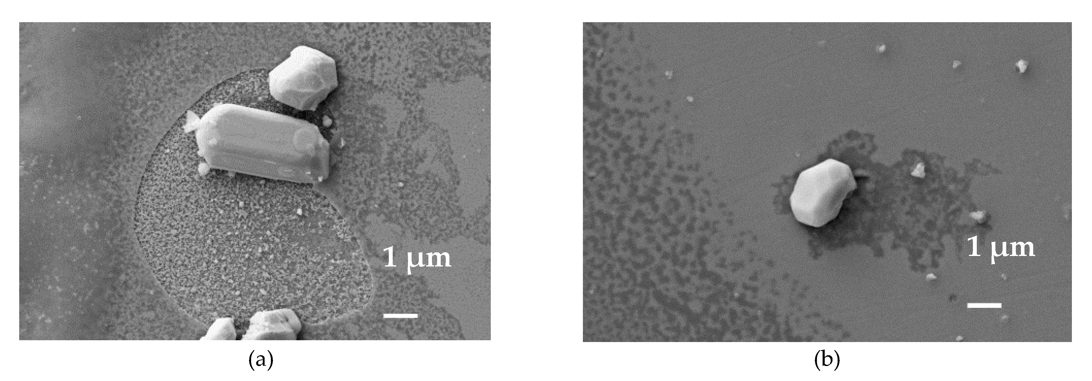
Figure 6 for a photograph of the mirrors after maximal oven exposure) due to higher sideways ingression of oxygen or moisture from the sample edge. Localized discrete points of degradation appeared in the bulk of the film and expanded with increased time at 400 °C. This is more pronounced in the sample prepared with the 12 A DC MS silver. The SEM picture in
Figure 7a shows a typical degradation patch from a protected 12 A DC MS silver system sample. The silver agglomerated causing rupturing of the top barrier layer coating and thus further localized accelerated agglomeration and thus larger degradation patches with time. The large crystal on the surface was silver. It was confirmed by Energy Dispersive X-ray analysis that the crystal was silver. The mechanism of corrosion was similar for the HiPIMS silver film systems. A typical example is shown in the SEM picture in
Figure 7b, for the 200 A HiPIMS sample after 768 h at 400 °C. Agglomeration of the silver took place, as seen for the DC MS; however, the pronounced rupturing of the barrier layer was not observed; thus, the points of degradation did not expand at an accelerated rate and hence resulted in smaller degradation points.
After 384 h, the 400 A HiPIMS silver system sample had visually degraded to be removed from the test. The nature of the degradation, although based on silver agglomeration, appeared different from the 12 A DC MS silver-based equivalent sample. The degradation patches for the 400 A HiPIMS based sample were smaller but occurred with higher frequency. In contrast, the 12 A DC MS samples exhibited larger corrosion patches, typified by the pronounced rupturing of the top barrier layer. The 12 A DC MS sample remained in the oven at 400 °C further until 768 h but, as can be observed from the photograph
Figure 6a, showed significant degradation and was subsequently removed from the test. The HiPIMS 200 A, however, remained visually good aside from the edge effect and scratches from the polished substrate until the end of the testing period of 1800 h. The HiPIMS 200 A silver in this thin film system is thus shown to be the most durable in the 400 °C oven.
4. Discussion
The main aim of the work was to determine whether HiPIMS silver films, used in a protected thin film system, could improve the performance of high temperature durable reflectors in comparison to the standard DC MS equivalent. In this context, the effect of the HiPIMS mode and sputter-parameters was investigated on the resulting silver films in comparison to the ‘baseline’ DC MS silver used in protected silver systems.
As reported [
7,
13], the as-deposited HiPIMS silver exhibited lower deposition rates per power density compared to DC MS. This was partially accounted for, as the HiPIMS silver grown here were also denser as a function of increasing peak current. The increase in density with peak current is a well-reported phenomenon [
14] and can be attributed to increased energy and thus mobility of ad-atoms due to an increased amount of ions in the deposition flux [
15]. Also reported [
16] but not measured here is that increasing the power density and ionized flux increases compressive stress in the silver films but without an increase in lattice defects.
The resistivity of the as-deposited HiPIMS silver films decreased slightly when increasing the peak target current from 100 A to 200A and was indeed lower (
Figure 2b) than the 12 A DC MS silver. The decrease may be due to an increase in film density as a function of peak current [
17].
The resistivity of the HiPIMS silver films, however, increased significantly when increasing further to 300 A and then 400 A to values higher than that of the reference 12 A DC MS silver. The resistivity is influenced by grain boundaries. A high number of grain boundaries and defects would reduce the efficiency of electron transport through the film, leading to a decrease in conductivity.
What was apparent was that the 200 A HiPIMS films had a similar grain size to the 12 A DC MS films. The grains had a higher degree of orientation and the film was much denser. The even denser 400 A HiPIMS film also showed a higher degree of grain orientation but a lower grain size. The film microstructure of the 400 A HiPIMS sample fits the extended Thornton model zone T [
13] where the high energy leads to high surface diffusion and the formation of a dense, finer grained film with highly orientated grains. A high nucleation density, which leads to small grain size, has previously [
18] been observed in HiPIMS and is enhanced by high ion currents towards the substrate surface. The increasing smaller grain size, exhibited at higher peak currents, thus increases the resistivity.
It seems that a competition between the two phenomena of the increasing density yet decreasing grain size occurred, where the highest conductivity under these sputter conditions occurred at 200 A in HiPIMS mode.
GIXRD and SEM showed that annealing the discrete silver films and the protected silver films led to grain growth and stronger orientation of the crystals. This, likewise, increased the conductivity for all the films presented here. Previous work [
19] shows that above a certain time and temperature (and dependent on the initial thickness of the silver) the conductivity drastically reduces discrete silver films due to voiding and segregation of the silver into separated agglomerates. In this work here, the temperature and time for the relatively thick 500 nm silver did not exceed this point and the silver remained as a network; thus, only an increase in conductivity was measured upon annealing due to the increased grain size.
The critical parameter for the high temperature reflectors is not electrical conductivity but reflectance. The relationship between conductivity and reflectance for highly conducting metals, such as silver was derived by Drude and confirmed experimentally by Hagens-Ruben [
20]. It was observed that, at higher wavelengths (lower frequencies), the optical constants of metals are similar to the values of Drude’s function, where the complex refractive index is much smaller than the damping constant or extinction coefficient. This leads to high reflectance. At higher wavelengths (near infra-red to infra-red) one can thus partially correlate the increase (or decrease) in reflectance to the same physical reasons as the observed increase in conductivity (i.e., film densification) or decrease in conductivity (i.e., increase in grain boundaries due to smaller grain sizes). The as-deposited discrete silver films exhibited this correlation: the reflectivity increased with increasing film conductivity.
At higher frequencies, deviations of Drude’s approach start to appear because bound electrons of the metal start to respond to the incidence of light instead of just valence band electron response. At 325 nm, there was a drop in the reflectivity of the films which correlated to an interband transition edge at 3.8 eV [
21]. The broadening of this edge, observable in the measured reflectance spectra, with the highest current HiPIMS silver films may be correlated to defect energy states caused by, e.g., grain boundaries or other defect or impurities. Indeed, the biggest deviation in the solar reflectance between the sputtered silver samples was at this edge in the UV-visible portion of the spectrum. This is where the most gain was exhibited by the 200 A HiPIMS films. In the UV/visible portion of the spectrum absorption via surface plasmons [
22], dependent on the surface geometry and size of the silver agglomerates on the surface, is also possible. This is particularly relevant for the discrete silver film post annealing. Clearly, from the SEM pictures of the annealed discrete silver films, the roughness increased and the surface geometry dramatically changed with annealing leading to the increased diffuse and decreased global solar reflectance.
For the protected silver film systems, the reflectance depended not only on the silver but also on the adhesion layers and barrier layers. As discussed previously in the results section, the benefits from the gain in the UV/visible portion of the spectra (around the interband transition edge) exhibited by the 200 A HiPIMS silver were not observable due to the interference effects and absorption of the metallic adhesion layer. The additional top barrier and adhesion layers were of course required as they limit the silver degradation. Thus, upon initially annealing, the protected silver film system grain growth occurred but without larger-scale agglomeration; thus, reflectance (and presumably the conductivity) increased.
Durability is defined in this context as minimized degradation in appearance and reflectance with increasing time at 400 °C. The 200 A HiPIMS silver system was more durable than the 12 A DC MS, whereas the 400 A HiPIMS silver system was less durable. The durability was determined by the whole film system, and it is beyond the scope of this paper to delve into the exact complex interplay between the film system and corrosion mechanism. The following aspects which affect the film stability are discussed: (1) The depositing flux during HiPIMS had a higher energy and higher ionized percentage, which would enhance the adhesion of the silver film to the substrate below, possibly improving durability. (2) The internal stress of the silver films, not measured here or even observed by a peak difference in the GIXRD, is reported [
16] to be higher for the HiPIMS films, effecting the adhesion and interaction with the top barrier layer. (3) What was measured is a peak shift in the GIXRD spectra towards higher Bragg angles for all silver films in the protected film system after annealing. This shift, which was larger for the HiPIMS silver systems, implies an increase in compressive stress in the protected silver film with annealing. (4) Finally, the reduced grain size of the 400 A HiPIMS silver may be detrimental to the film stability (higher diffusion paths, increased free energy).
