1. Introduction
Tunable complex oxide thin films are one of the leading candidates to become a core technology in the new generation of phase shifters, tunable filters, and other components for communications and radar devices at radio frequency (RF), microwave (MW), and higher frequencies. This is due to their temperature and frequency stability, low-tuning voltages, relatively low losses, cost, and their fast response [
1,
2]. Postprocessing of tunable complex oxide thin films became a common practice to establish or improve dielectric properties of these films [
3] grown by such methods as metallo-organic solution deposition (MOSD) [
4], RF magnetron sputtering [
5,
6,
7,
8,
9], metal–organic chemical vapor deposition (MOCVD) [
10], and others. In addition to improving the crystallinity of the thin films, this postgrowth processing allows augmenting of the oxygen deficiency in the films through various approaches [
11]. For Ba
xSr
1−xTiO
3 thin films, the crystallization temperature used to improve the grown films is typically between 700 °C and 800 °C [
12]. Typically, this postprocessing occurs in a furnace with oxygen flow for extended amounts of time (normally about an hour or more) [
13].
The purpose of this research was to determine applicability of postprocessing BaSrTiO
3 thin films with microwave radiation as an alternative way to enhance dielectric properties of the thin films. We anticipated three potential benefits of utilizing the microwave postprocessing in comparison with conventional furnace annealing. Firstly, as opposed to heating in a conventional furnace, heating using microwave radiation is volumetric, namely, the entire sample volume is heated simultaneously [
14]. This could enable novel approaches to tailoring the meso- and micro-structure of the films, such as growing an initially amorphous multilayered structure, where some layers of the film are susceptible to a MW field and others are transparent, which may create heterogeneous structures that yield significantly enhanced properties for the film such as minimized leakage current [
15]. These structures are not easily achieved in a conventional furnace. It is worth mentioning that in this work, we were using an additional silicon carbide (SiC) susceptor underneath the substrate and, therefore, we did not explore this approach here due to additional heating from the bottom of the film. Secondly, the time required for the postprocessing of the thin films could be significantly shorter due to the effects of an electromagnetic (EM) field on the crystallization process. For example, it was determined [
16] that a direct current (DC) or alternating current (AC) field increases the sintering rate in a green body of a bulk ceramic material. Thirdly, there is a push to integrate the components that include tunable complex oxides into Si-based integrated circuits [
17]. However, the crystallization temperature of the complex oxide thin films is in the range of 700–800 °C. In order to make these components Si CMOS (complementary metal–oxide semiconductor) compatible, we needed to reduce this temperature to values below 550 °C [
18]. This was our first attempt to investigate if significant enhancement of dielectric properties of the tunable complex oxide thin films can be achieved when the film is postgrowth treated in microwaves.
2. Materials and Methods
A thin film of BaSrTiO3 (BST) with a nominal composition of Ba0.6Sr0.4TiO3 (designated as 60/40) was grown by rf magnetron sputtering on a platinized silicon wafer under the following conditions. The Si wafer orientation was (100) with a 5000 Angstrom SiO2 layer thermally grown from the vendor (Nova Electronic Materials). The DC/RF sputtering system was pumped to a base pressure of 3 × 10⁻⁸ Torr. The wafer was cleaned in situ using an Ar plasma at 50 W RF and 10 m Torr Ar for 5 min. The wafer was then heated to 350 °C, and a Ti adhesion layer and a Pt bottom electrode film were deposited sequentially. The BST 60/40 film was then deposited at a pressure of 10 m Torr (using an Ar/O2 ratio of 90/10). The BST growth rate was determined to be about 0.7 nm/min using a target power density of 21.2 W/in2. After deposition, the sample was immediately cooled at 10 °C/min in the same 10 mTorr Ar/O2 ambient used for deposition.
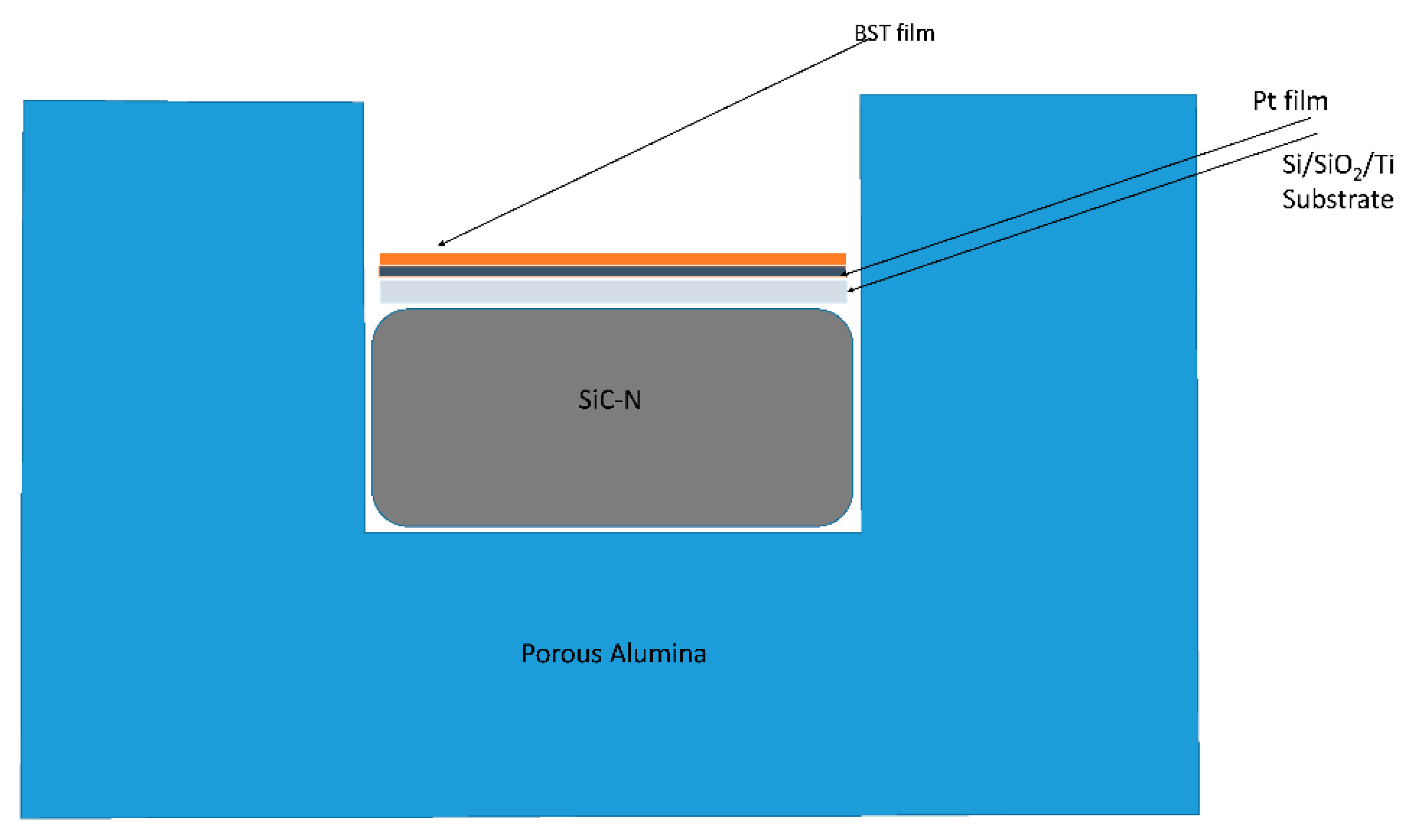
The BST growth temperature was kept low, well below 550 °C, to maintain temperature compatibility with Si complementary metal-oxide-semiconductor (CMOS) and in order to investigate the effects of the microwave field on the crystallization of the film. The thin film sample was divided into three parts. One part was kept “as-deposited” for the reference and the other two parts were treated in the microwave (MW) field using an Anton Paar Multi-Pro multimode system operating at 2.45 GHz for 10 min each at 500 W and 1000 W, respectively. It was shown that the microwave susceptibility of certain materials increases with the sample temperature, and therefore, in order to enhance the effects of the MW postprocessing of the films, the sample was placed on a SiC MW susceptor to enhance the effects of the MW treatment with combined ohmic heating of the sample. The entire assembly was placed in a thermally insulating crucible built from porous alumina as shown in
Figure 1. The SiC susceptor reached its maximum temperature of 700 ± 20 °C as measured by optical pyrometer within 3 min of the run.
The reference thin film sample and the two thin film samples postprocessed with the MW field were characterized for physical and structural information using X-ray diffraction (XRD), X-ray reflectivity (XRR) (D8 Discover, Bruker AXS, Karlsruhe, Germany), scanning electron microscopy (SEM) (Nova Nano 600, FEI, Hillsboro, Oregon, OR, USA), and atomic force microscopy (AFM) (Bruker Nano, Karlsruhe, Germany), and characterization of the dielectric properties was measured using RF probing. Dielectric properties were characterized at 100 kHz using a metal–insulator–metal (MIM) configuration whereby the Pt thin film underneath of the BST film served as a bottom (ground) electrode. Circular Pt electrodes 200 microns in diameter were deposited, via a shadow mask, on top of the BST thin film to serve as top electrodes.
3. Results and Discussion
3.1. Thin Film Microstructure Characterization
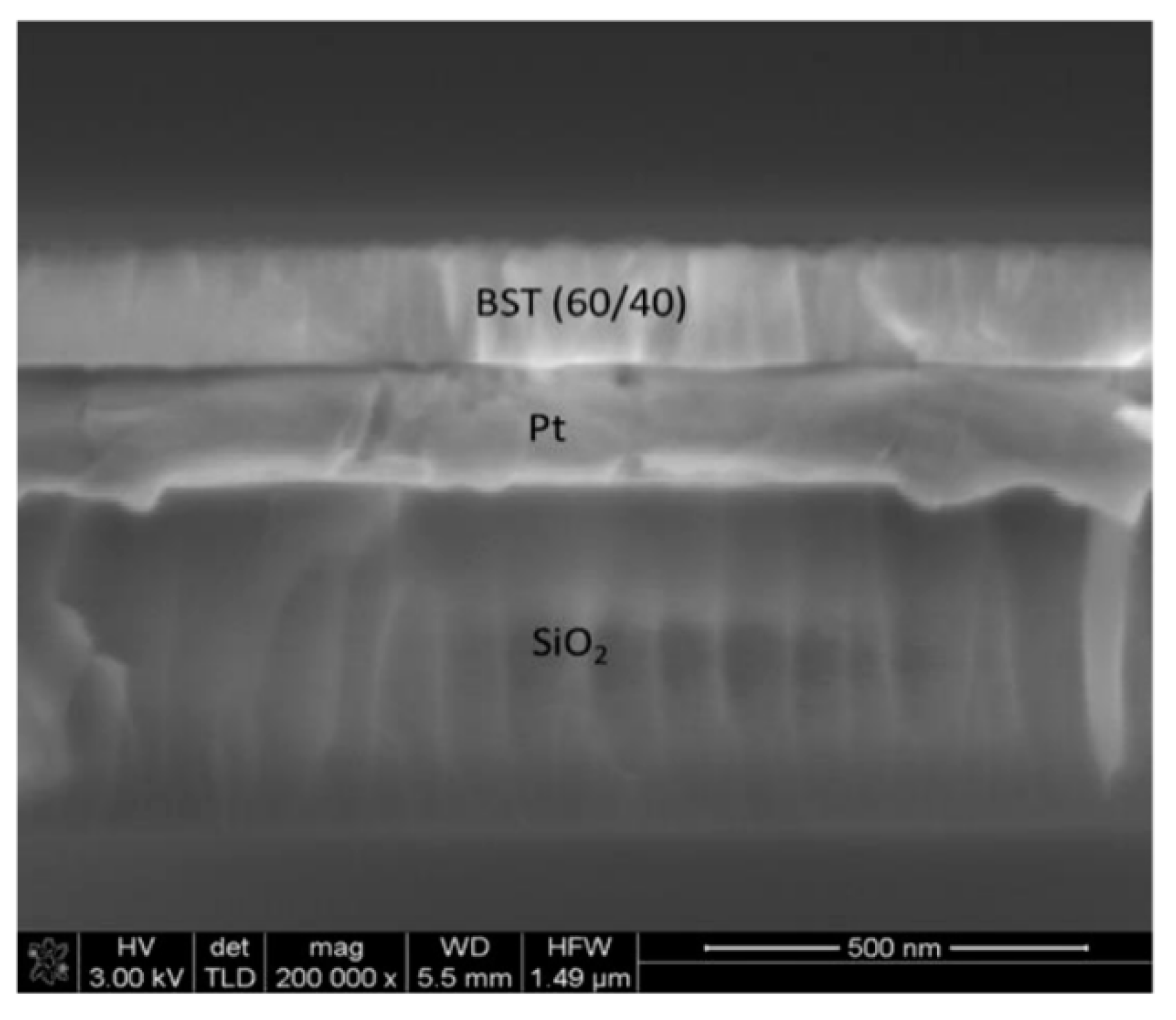
The 170 nm thick BST 60/40 thin film was grown on Si/SiO
2/Ti/Pt substrate under the conditions described in
Section 2. The cross-section of the film is shown in
Figure 2:
The Pt bottom electrode film was determined to be 170 nm and the Ti adhesion layer was under 3 nm thick. After the sample was obtained, it was split into three parts. One was retained as a reference and the other two parts were processed in the MW chamber as described in
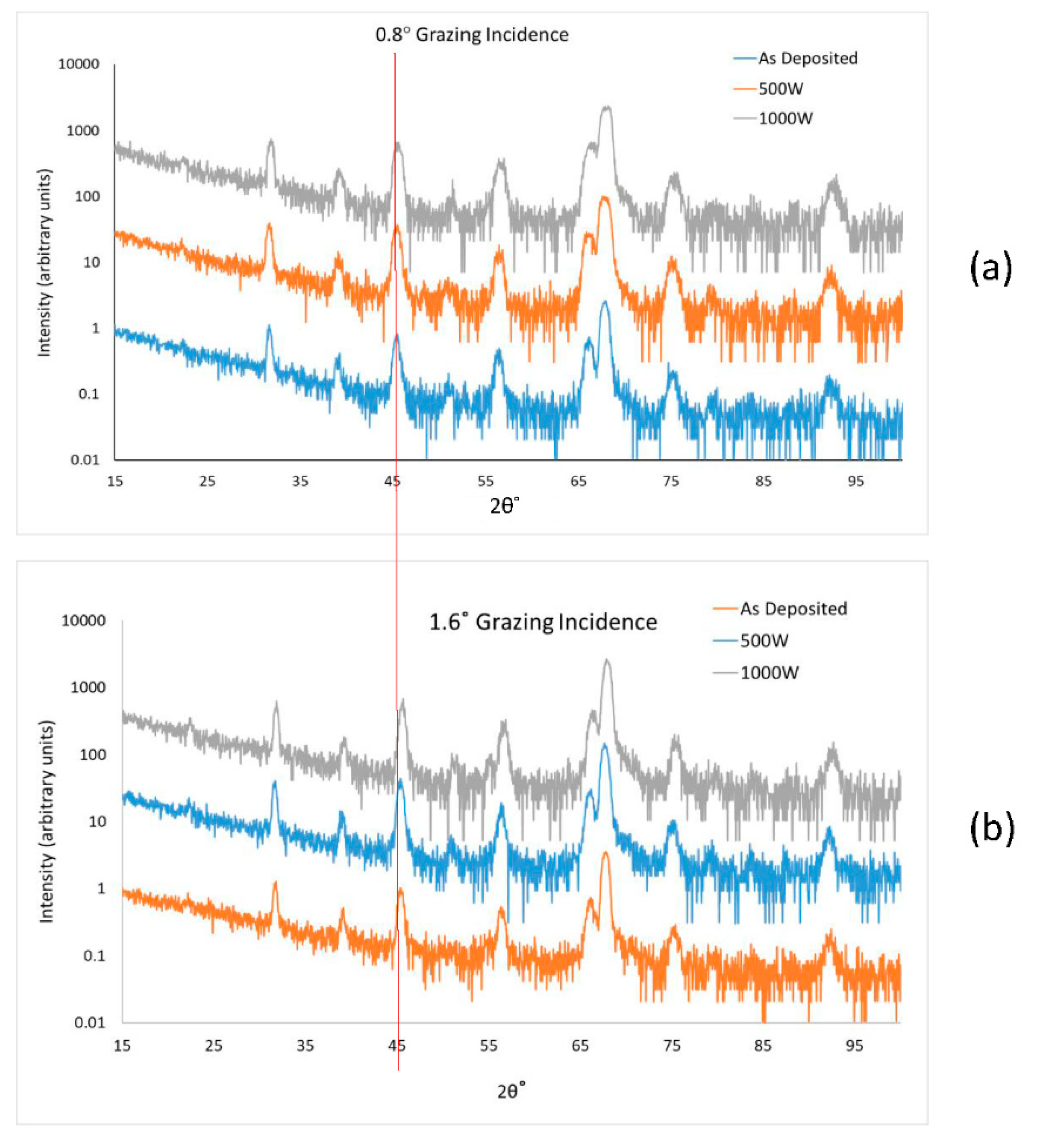
Section 2. The XRD data for the three samples, the ‘as-deposited’ reference and MW processed samples, are presented in
Figure 3.
The samples were measured in grazing-incidence geometry to enhance the diffraction signal from the BST thin film and to potentially probe differences in crystallinity through the thickness of the film. Scans with fixed incident angles of 0.8° and 1.6° are shown in
Figure 3a,b, respectively. The ‘as-deposited’ film is polycrystalline without definitive signs of texturing, which results from the low deposition temperature used for the BST. The processed films remain similarly polycrystalline after the MW annealing.
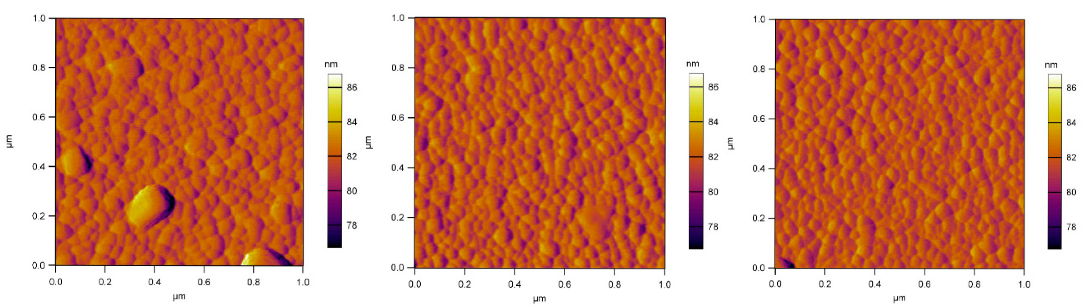
Further, the AFM surface topography scans are presented in
Figure 4:
3.2. Thin Film Dielectric Properties
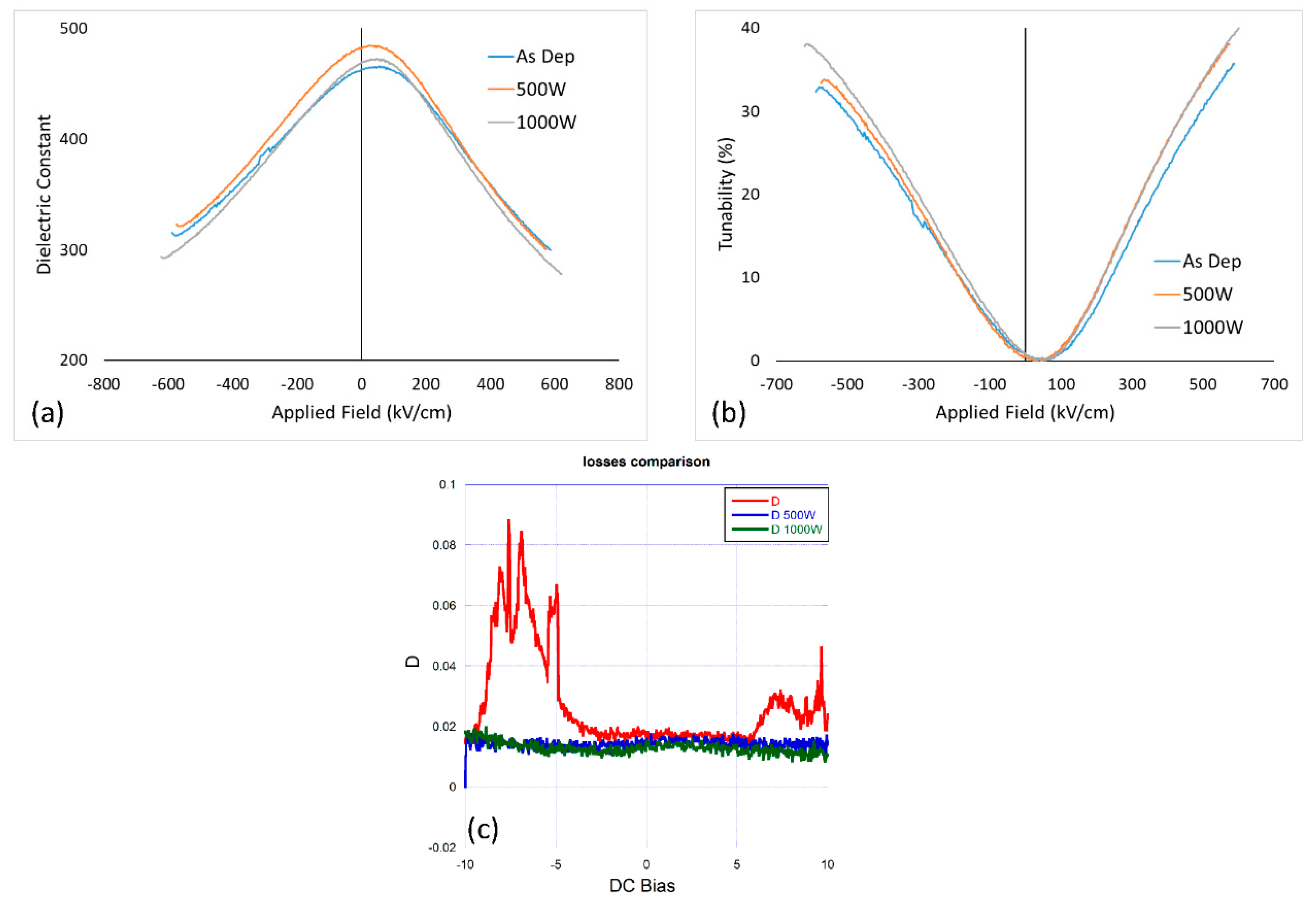
The measured dielectric properties are presented in
Figure 5 and
Figure 6.
Figure 5a,b show the plots that compare dielectric constant and tunability of the three thin films under investigation. Dielectric tunability,
, is defined here as the percent change in small-signal capacitance with applied DC bias, so that
, where
is the dielectric constant of BST at zero-bias, and
is the dielectric constant of BST at a specified value of DC bias. Tunabilities were calculated using dielectric constant values at 600 kV/cm fields.
Figure 5c is a comparison of the measured dielectric loss extracted from the same measurements.
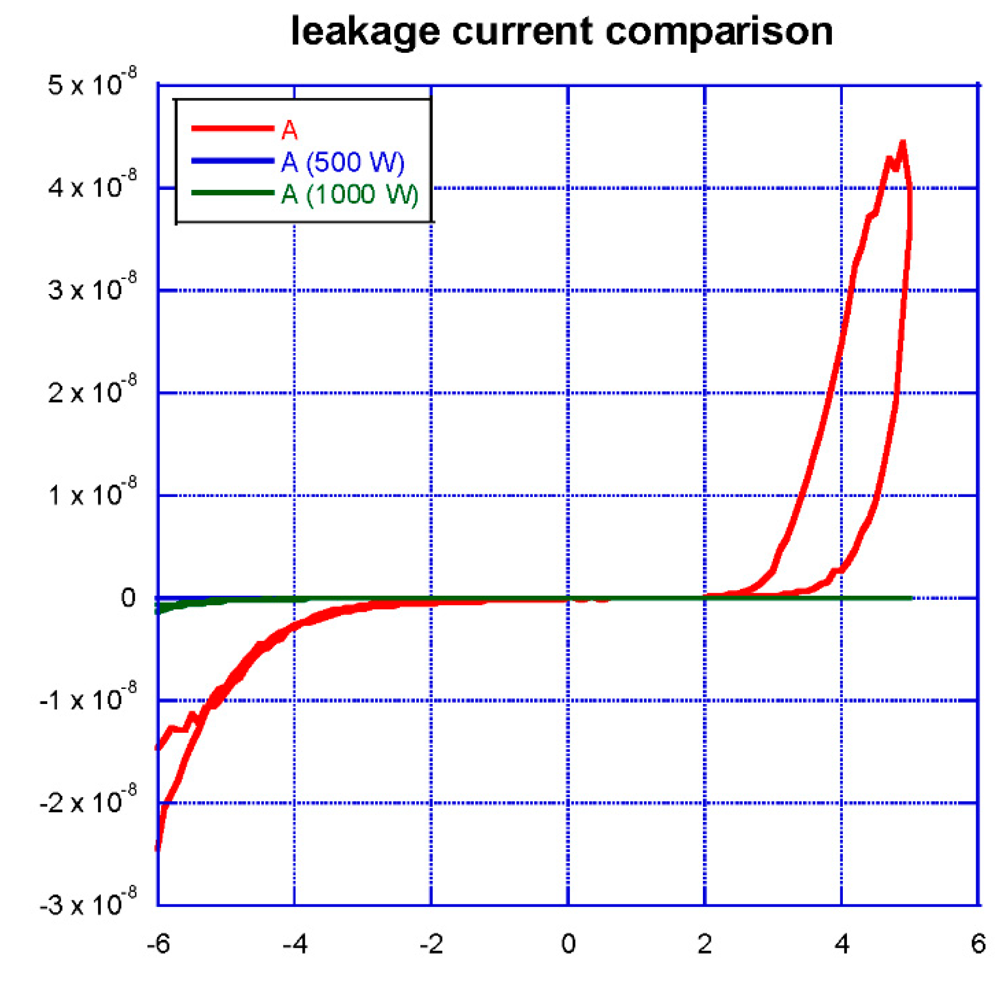
Another important property for the BST tunable thin films needed for consideration as a core technology for communications devices is leakage current. Leakage current here is defined as the I–V response through the thickness of the film showing how much current in drawn through the metal-insulator-metal (MIM) at various applied voltages. Lower leakage is one mechanism representative of lower parasitic power loss through the device.
Figure 6 presents a comparison between the leakage current data from the three samples under consideration.
The results in
Figure 5 and
Figure 6 demonstrate progressive improvement of the dielectric properties of the tunable complex oxide thin films with increasing applied power of the postgrowth microwave field. The values of the dielectric constant obtained in this work (470–480 at zero bias) are comparable with values cited in the literature for similar systems [
6,
9]. Although the increase in tunability of the film is not significant (38% for the film treated with 1000 W microwave field vs. 32% for untreated film), the dielectric loss and leakage current when the film is biased show progressive significant improvement for the films that were postgrowth treated with an MW field at 500 and 1000 W, respectively.
3.3. Discussion of the Obtained Results
In order to understand this phenomenon, we discuss potential contributors to the results presented above.
It is known [
19] that the presence of MW during sintering of bulk ceramics inhibits grain growth. We estimate that a similar effect is taking place in our thin film system when MW field is applied during postprocessing. AFM scans (
Figure 4) support this assessment presenting with a modest decrease in the grain size as a function of MW processing power and compared with the as-deposited film (from 45 nm average to 40.6 nm average). In addition, comparison of grazing angle XRD (
Figure 3a,b) scans for 0.8° and for 1.6° shows a significantly higher percentage of increase in the width of full width half max (FWHM) for 0.8°, in comparison with 1.6°, when the peaks for the same incident angle are compared at 0 W and 1000 W applied (
Table 1 and
Table 2). This interesting fact noted for the three most prominent XRD peaks indicates some differences in microstructure between the bottom and the top of the thin films treated with the MW field. Expansion of the FWHM width is typically indicative of a decrease in the grain size in the BST film [
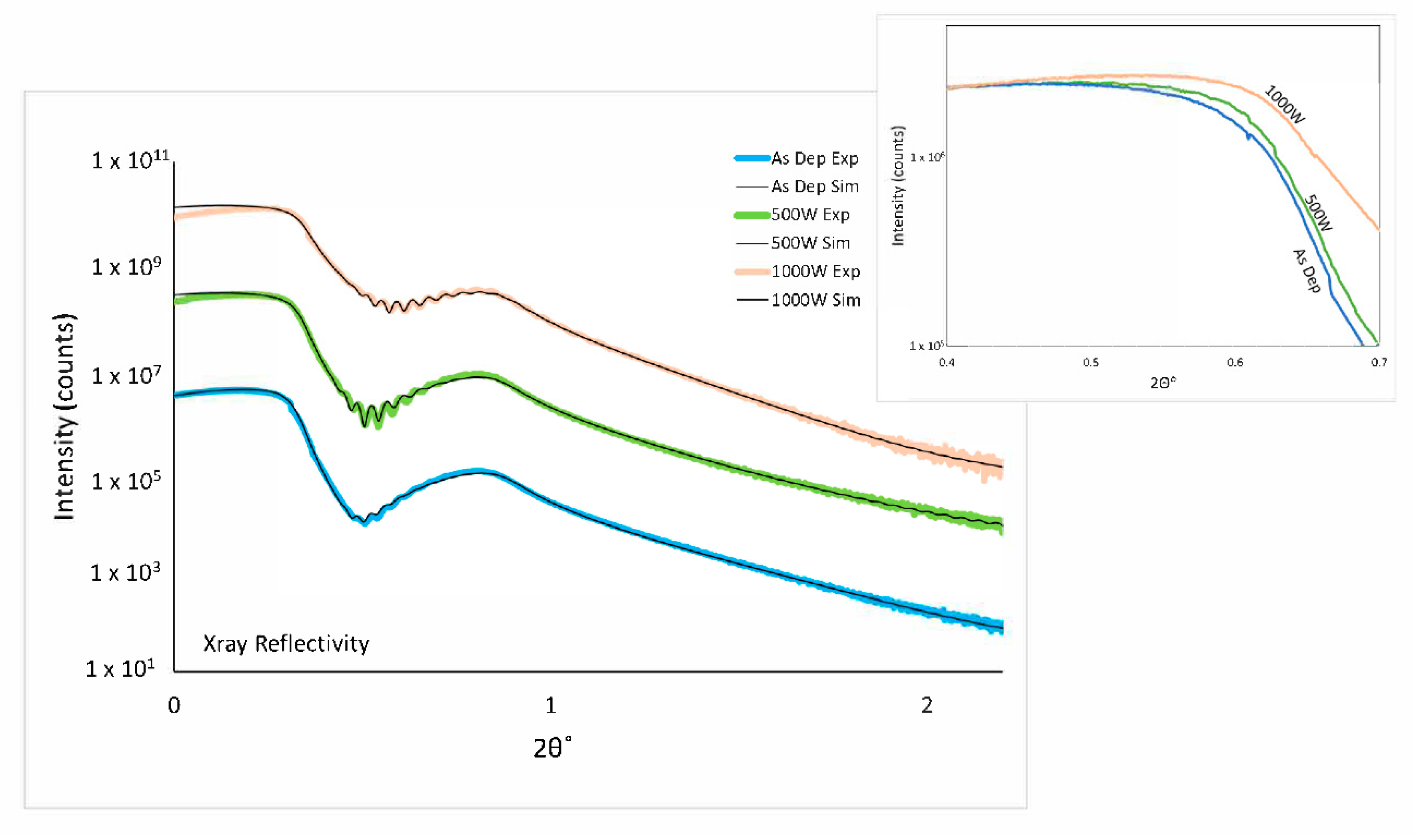
20]. This discrepancy could be due to the fact that the bottom of the film is in closer proximity to the susceptor and, hence, the effects associated with the crystallization due to the susceptor heating compete in a more prominent way with the effects associated with the MW field heating of the film that include inhibited grain growth. This indicates possible additional crystallization enhancement near the substrate, which is logical to assume since we are using an MW susceptor located under the substrate. In addition, X-ray reflectometry (XRR) has been performed on the films under investigation and simulated using Leptos version 7.8 software (Bruker Nano Inc., Billerica, MA, USA) (
Figure 7).
The results of XRR showed a consistent increase of the film density from the as-deposited film to the film postgrowth processed in MW at 1000 W as shown in
Table 3.
The increased density of the films with increased power of postgrowth MW processing may indicate possible filling of oxygen vacancies typically present in the BST films after RF sputtering deposition at relatively low temperatures. This argument may be further supported by the visible shift to higher 2θ of the XRD peaks of the sample treated at 1000 W in comparison with as-deposited at 1.6° indicating lattice contraction. Reduction of oxygen vacancies further improves dielectric properties of the deposited thin film.
Lastly, we speculate that, as in the case with conventional furnace postprocessing of the films, exposure of the stack of substrate/bottom electrode/BST film to MW processing and heat enhanced the interfacial contact between the bottom electrode and the BST thin film. Enhancement of the contact, which includes reduction of the defects, such as oxygen vacancies, typically results in improvements in the dielectric properties of the films, including leakage current and dielectric loss [
21].
4. Conclusions
A new approach to postgrowth processing of BST thin films has been demonstrated and discussed where the films grown by RF sputtering at relatively low temperature were postprocessed in an MW multimode chamber in the field at 500 and 1000 W. The results showed a modest improvement in the value of the tunability but significant improvement in the values of dielectric losses when the film is biased in an MIM structure and significant improvement in the values of the leakage current. These improvements were attributed to such factors as enhancement in crystallization at the bottom of the BST thin film, filling of some oxygen vacancies, and improved contact between bottom electrode and the BST thin film. The improvements in the dielectric properties of the processed films are consistent with conventional postgrowth processing methods (such as a conventional oven with oxygen flow). Therefore, the proposed method can be presented as a candidate to substitute the conventional methods with a goal to reduce processing time and simplify the process. However, the main attraction of the proposed method is in a new capability that it presents. Namely, it has been shown in this work that the utilization of MW can lead to selective crystallization of certain layers of the film in the direction of the deposition which is unattainable with the conventional postgrowth processing methods. This effect indicates that the proposed method, if executed correctly, is potentially capable of fabricating a film with controlled crystallinity (from amorphous to highly crystalline) in the direction of deposition which can yield significant flexibility to tailor mechanical, optical, and dielectric properties of the film. This effect cannot be achieved with conventional postgrowth processing such as furnace annealing.
These results could lead to fabrication of the films that will have superior dielectric properties, such as leakage current and dielectric losses in comparison with the films postgrowth processed with the conventional methods.
Author Contributions
Concept, D.S. and M.P.I.; thin film deposition, M.P.I.; microwave processing, D.S. and J.F.C.; XRD characterization, M.P.I; SEM characterization, S.G.H.; AFM characterization, C.W.H.; dielectric properties characterization, E.H.N.; analysis, D.S. and M.P.I.
Funding
This research received no external funding.
Conflicts of Interest
The authors declare no conflict of interest.
References
- Cole, M.W.; Nothwang, W.D.; Demaree, J.D.; Hirsch, S. Integration of Ba1−xSrxTiO3-based active thin films with silicon-compatible materials and process science protocols to enable affordable on-the-move communications technologies. J. Appl. Phys. 2005, 98, 024507. [Google Scholar] [CrossRef]
- Shreiber, D. Microwave and THz Metamaterial-Based Devices for Potential Applications in NDE, Chem-Bio Detection and Dielectric Characterization of Complex Oxide Thin Films. In Metamaterials-Devices and Applications; Lucas Borja, A., Ed.; IntechOpen: London, UK, 2017. [Google Scholar]
- Kim, S.G.; Mah, S.B.; Jang, N.W.; Paik, D.S.; Park, C.Y. Post-annealing in oxygen ambient for (Ba,Sr)TiO3 thin films prepared by pulsed laser deposition. Mater. Lett. 2000, 43, 254–258. [Google Scholar] [CrossRef]
- Mansour, A.; Hmeda, M.; Kalkur, T.S.; Alpay, P.; Sbockey, N.; Tompa, G.S. Switchable Band Pass BAW Filter Based on Ba0.7Sr0.3TiO3 for C Band RF Applications. In Proceedings of the 2015 Joint IEEE International Symposium on the Applications of Ferroelectric (ISAF), International Symposium on Integrated Functionalities (ISIF), and Piezoelectric Force Microscopy Workshop (PFM), Singapore, 24–27 May 2015. [Google Scholar]
- Tsai, M.S.; Sun, S.C.; Tseng, T.Y. Effect of oxygen to argon ratio on properties of (Ba,Sr)TiO3 thin films prepared by radio-frequency magnetron sputtering. J. Appl. Phys. 1997, 82, 3482. [Google Scholar] [CrossRef]
- Kiselev, A.; Afanasiev, M.S.; Levashov, S.A.; Sivov, A.A.; Chucheva, G.V. Thickness dependence of electrical and piezoelectric properties of ferroelectric Ba0.8Sr0.2TiO3 thin films. Thin Solid Films 2016, 619, 214–219. [Google Scholar] [CrossRef]
- Afanasiev, S.; Kiselev, D.A.; Levashov, S.A.; Luzanov, V.A.; Nabiyev, A.A.; Naryshkina, V.G.; Sivov, A.A.; Chucheva, G.V. The Influence of the Substrate Material on the Structure and Electrophysical Properties of BaxSr1–xTiO3 Thin Films. Phys. Solid State 2018, 60, 954–957. [Google Scholar] [CrossRef]
- Chen, X.Y.; Xu, Z.P.; Yan, D.X.; Fan, Y.S.; Zhu, J.G.; Yu, P. Great enhancement of polarization in the (Ba0.67Sr0.33TiO3/LaNiO3) n multilayer thin films. J. Alloys Compd. 2017, 695, 1913–1917. [Google Scholar] [CrossRef]
- Pervez, N.K.; Hansen, P.J.; York, R.A. High tunability barium strontium titanate thin films for rf circuit applications. Appl. Phys. Lett. 2004, 85, 4451. [Google Scholar] [CrossRef]
- Shreiber, D.; Cole, M.W.; Enriquez, E.; Hirsch, S.G.; Ngo, E.; Hubbard, C.; Ivill, M.; Chen, C. Some unusual behavior of dielectric properties of SrTiO3 metal organic chemical vapor deposition grown thin films. J. Appl. Phys. 2014, 116, 094101. [Google Scholar] [CrossRef]
- Podpirka, A.; Cole, M.W.; Ramanathan, S. Effect of photon irradiation on structural, dielectric, and insulating properties of Ba0.60Sr0.40TiO3 thin films. Appl. Phys. Lett. 2008, 92, 212906. [Google Scholar]
- Zhua, H.; Miaoa, J.; Nodab, M.; Okuyama, M. Preparation of BST ferroelectric thin film bymetal organic decomposition for infrared sensor. Sens. Actuators A Phys. 2004, 110, 371–377. [Google Scholar] [CrossRef]
- Cole, M.W.; Joshi, P.C.; Hubbard, C.W.; Ngo, E. Material Properties of MOSD Derived Ba1-xSrxTiO3-Based Thin Films for Pyroelectric Sensor Applications. Integr. Ferroelectr. 2006, 83, 99–111. [Google Scholar] [CrossRef]
- Pinheiro, L.B.; Tabuti, F.N.; Martinelli, A.E.; Fonseca, F.C. Influence of microwave-assisted hydrothermal treatment on theproperties of nickel oxide–zirconia based composites. Ceram. Int. 2016, 42, 9058–9064. [Google Scholar] [CrossRef]
- Cole, M.W.; Ivill, M.P.; Shreiber, D. Enabling Artificial Thin Film Material Structures of Non-linear Complex Oxide Thin Films. U.S. Patent Application US15/788,972, 26 April 2018. [Google Scholar]
- Conrad, H.; Yang, D. Effect of the strength of an AC electric field compared to DC on the sintering rate and related grain size of zirconia (3Y-TZP). Mater. Sci. Eng. A 2013, 559, 591–594. [Google Scholar] [CrossRef]
- Sedky, S.; Witvrouw, A.; Bender, H.; Baert, K. Experimental determination of the maximum post-process annealing temperature for standard CMOS wafers. IEEE Trans. Electron Devices 2001, 48, 377–385. [Google Scholar] [CrossRef]
- Warusawithana, M.P.; Cen, C.; Sleasman, C.R.; Woicik, J.C.; Li, Y.; Kourkoutis, L.F.; Klug, J.A.; Li, H.; Ryan, P.; Wang, L.P.; et al. A Ferroelectric Oxide Made Directly on Silicon. Science 2009, 324, 367–370. [Google Scholar] [CrossRef] [PubMed]
- Menezes, R.R.; Souto, P.M.; Kiminami, R.H.G.A. Microwave Fast Sintering of Ceramic Materials. In Sintering of Ceramics—New Emerging Techniques; Lakshmanan, A., Ed.; InTech: London, UK, 2012. [Google Scholar]
- Remmel, T.; Gregory, R.; Baumert, B. Characterization of barium strontium titanate thin films using XRD. Adv. X-Ray Anal. 1999, 41, 38–45. [Google Scholar]
- Tamura, T.; Takai, K.; Noshiro, H.; Kimura, M.; Otani, S.; Yamada, M. Influence of Electrode Contacts on Leakage Current of SrTiO3 Capacitors. Jpn. J. Appl. Phys. 1994, 33, 1697–1699. [Google Scholar] [CrossRef]
© 2019 by the authors. Licensee MDPI, Basel, Switzerland. This article is an open access article distributed under the terms and conditions of the Creative Commons Attribution (CC BY) license (http://creativecommons.org/licenses/by/4.0/).


