Photocatalytic Activity and Stability of Porous Polycrystalline ZnO Thin-Films Grown via a Two-Step Thermal Oxidation Process

Abstract
:1. Introduction
2. Experiment
3. Film Growth and Characterization
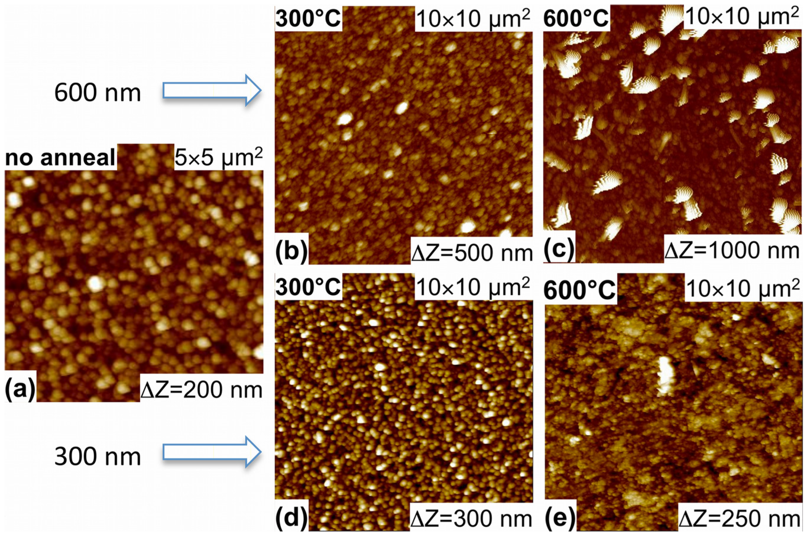
3.1. Morphology and Structure

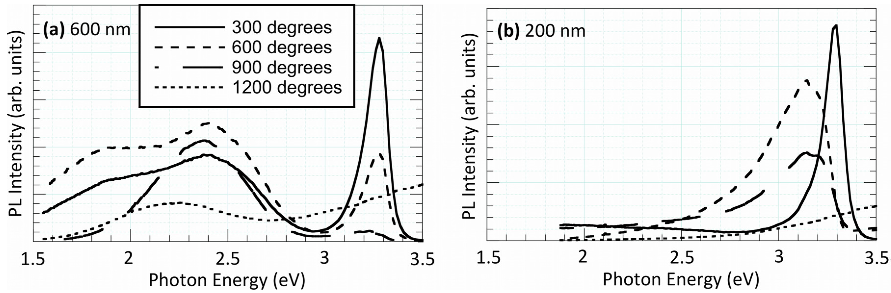
3.2. Optical Properties

4. Surface Catalysis and Reaction Kinetics
5. Results
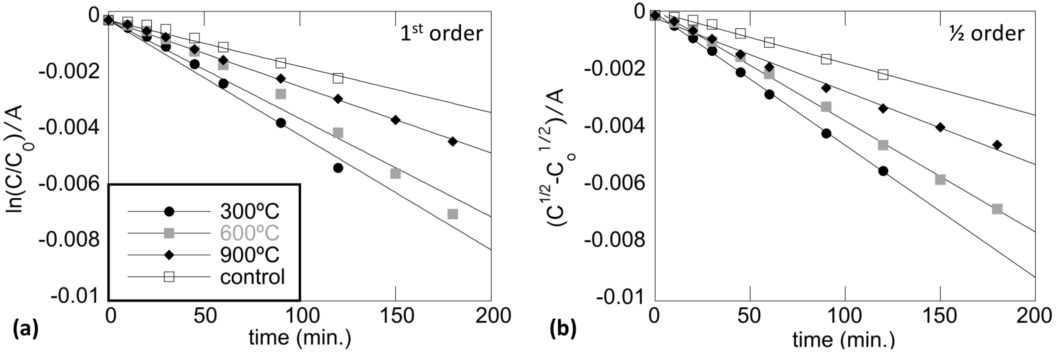
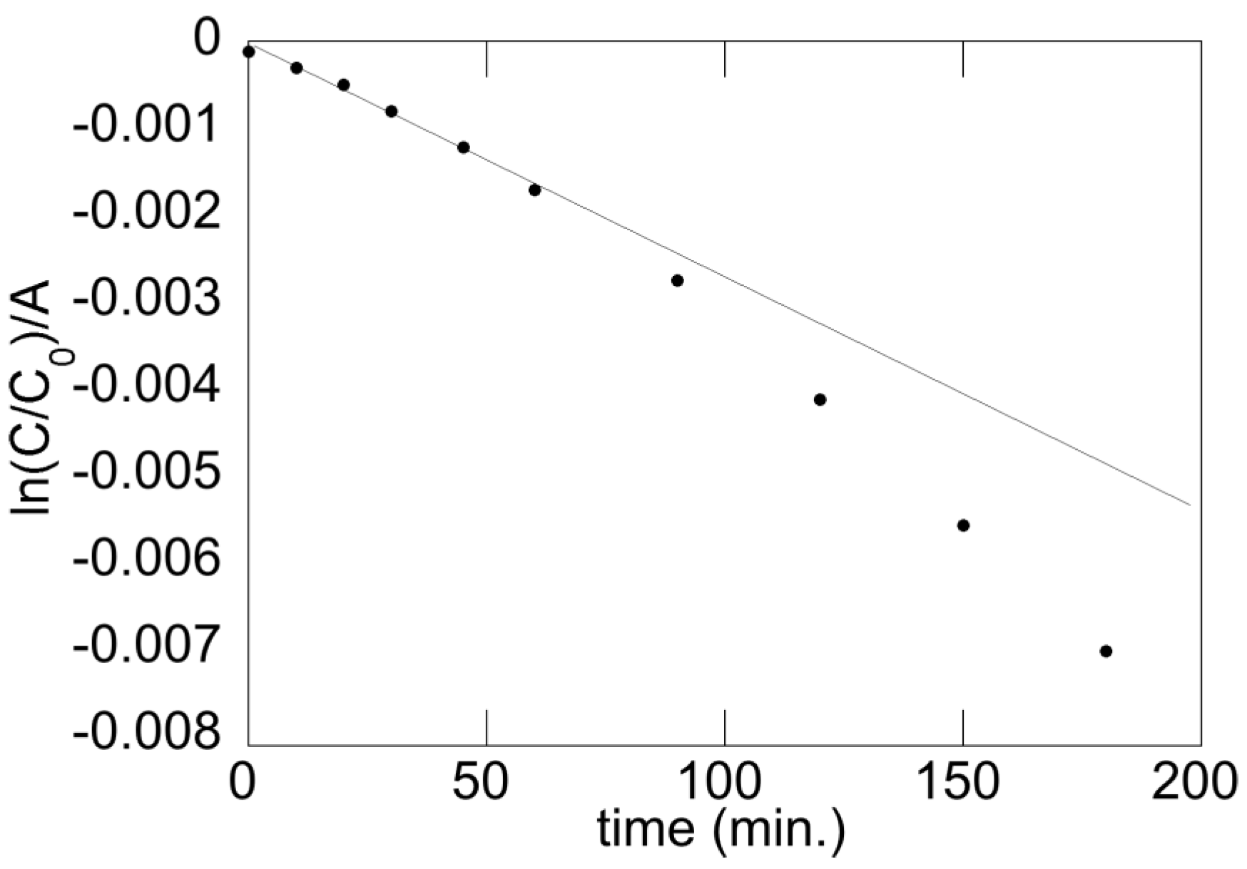
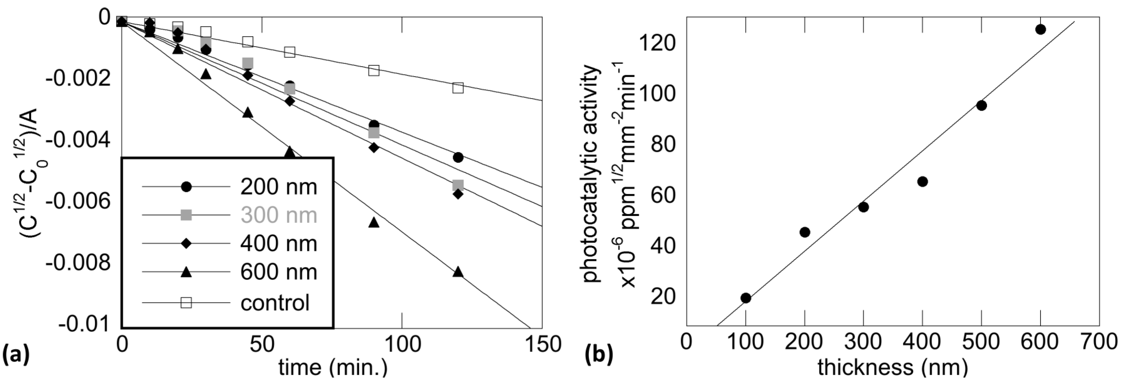
5.1. Reaction Order


| Annealing Temperature (°C) | 1st order | half-order |
|---|---|---|
| 300 | 0.999 | 0.856 |
| 600 | 0.998 | 0.887 |
| 900 | 0.993 | 0.886 |

5.2. Photocatalytic Activity and Annealing Temperature
| Annealing temperature (°C) | Photocatalytic activity (ppm1/2mm-2min-1) |
|---|---|
| 300 | |
| 600 | |
| 900 |
5.3. Photocatalytic Activity and Film Thickness
| Film thickness (nm) | Photocatalytic activity (ppm1/2mm-2min-1) |
|---|---|
| 100 | |
| 200 | |
| 300 | |
| 400 | |
| 500 | |
| 600 |
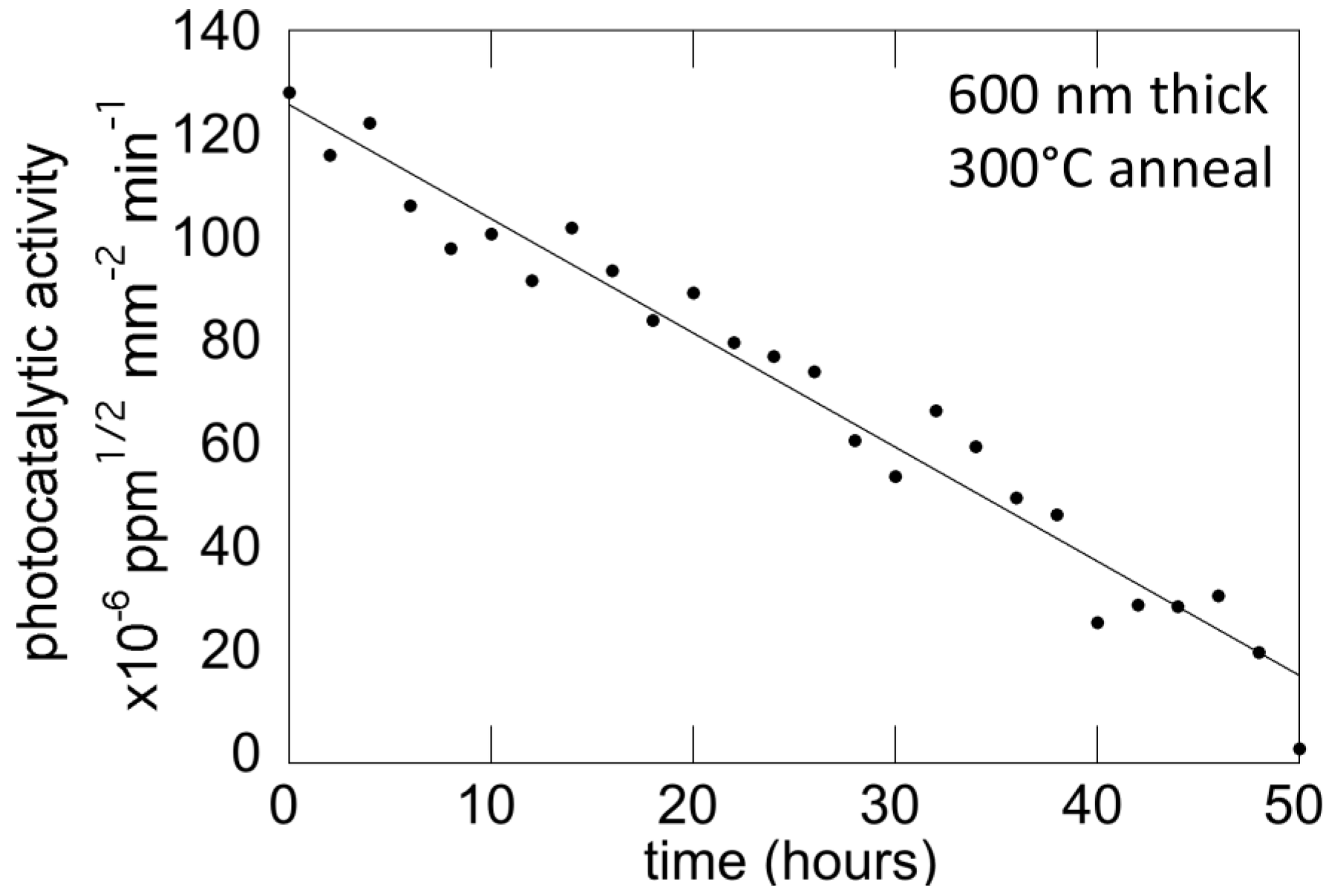
5.4. Film Stability

6. Discussion
7. Conclusions
Acknowledgments
Author Contributions
Conflicts of Interest
References
- Ozgur, U.; Alivov, Y.; Liu, C.; Teke, A.; Reshchikov, M.; Dogan, S.; Avrutin, V.; Cho, S.; Morkoc, H. A comprehensive review of ZnO materials and devices. J. Appl. Phys. 2005, 98. [Google Scholar] [CrossRef]
- Zhao, Q.; Xie, Y.; Zhang, Z.; Bai, X. Size-selective synthesis of zinc sulfide hierarchical structures and their photocatalytic activity. Cryst. Growth Des. 2007, 7, 153–158. [Google Scholar] [CrossRef]
- Diebold, U. Structure and properties of TiO2 surfaces: A brief review. Appl. Phys. A 2003, 76, 681–687. [Google Scholar] [CrossRef]
- Moore, J.; Kenny, S.; Baird, C.; Morkoc, H.; Baski, A. Electronic behavior of the Zn- and O-polar ZnO surfaces studied using conductive atomic force microscopy. J. Appl. Phys. 2009, 105. [Google Scholar] [CrossRef]
- Covington, L.; Moore, J. Photoconductivity and transient response of Al:ZnO:Al planar structures fabricated via a thermal oxidation process. Thin Solid Films 2013, 506, 106–111. [Google Scholar] [CrossRef]
- Moore, J.; Thompson, C. A phenomenological model for the photocurrent transient relaxation observed in ZnO photodetector devices. Sensors 2013, 13, 9921–9940. [Google Scholar] [CrossRef] [PubMed]
- Ali, G.; Thompson, C.; Jasim, A.; Abdulbaki, I.; Moore, J. Effect of embedded Pd microstructures on the flat-band-voltage operation of room temperature ZnO-based propane gas sensors. Sensors 2013, 13, 16801–16815. [Google Scholar] [CrossRef]
- Ali, G.; Kadhim, A.; Thompson, C.; Moore, J. Electrical and optical effects of Pd microplates embedded in ZnO thin film based MSM UV photodetectors: A comparative study. Sens. Actuators A 2014, 209, 16–23. [Google Scholar] [CrossRef]
- Moore, J.; Covington, L.; Foster, R.; Gee, E.; Jones, M.; Morris, S. ZnO ultraviolet photodetectors grown via thermal oxidation of Zn-metal on glass and sapphire substrates. Proc. SPIE 2011, 7940. [Google Scholar] [CrossRef]
- Gedamu, D.; Paulowicz, I.; Kaps, S.; Lupan, O.; Wille, S.; Haidarschin, G.; Mishra, Y.K.; Adelung, R. Rapid Fabrication Technique for Interpenetrated ZnO Nanotetrapod Networks for Fast UV Sensors. Adv. Mater. 2014, 26, 1541–1550. [Google Scholar] [CrossRef] [PubMed]
- Antoine, T.E.; Mishra, Y.K.; Trigilio, J.; Tiwari, V.; Adelung, R.; Shukla, D. Prophylactic, therapeutic and neutralizing effects of zinc oxide tetrapod structures against herpes simplex virus type-2 infection. Antivir. Res. 2010, 96, 363–375. [Google Scholar] [CrossRef] [PubMed]
- Hashimoto, K.; Irie, H.; Fujishima, A. TiO2 Photocatalysis: A Historical Overview and Future Prospects. Jpn. J. Appl. Phys. 2005, 44, 8269–8285. [Google Scholar] [CrossRef]
- You, H.C.; Lin, Y.H. Investigation of the Sol-Gel Method on the Flexible ZnO Device. Int. J. Electrochem. Sci. 2012, 7, 9085–9094. [Google Scholar]
- Moore, J.; Louder, R.; Covington, L.; Stansell, R. Photoconductivity and photocatalytic activity of ZnO thin films grown via thermal oxidation. Proc. SPIE 2012, 8263. [Google Scholar] [CrossRef]
- Oppenlander, T. Photochemical Purification of Water and Air; Wiley-VCH: Weinheim, Baden-Württemberg, 2003. [Google Scholar]
- Anpo, M. Utilization of TiO2 photocatalysts in green chemistry. Pure Appl. Chem. 2000, 72, 1265–1270. [Google Scholar] [CrossRef]
- Bian, S.; Mudunkotuwa, I.; Rupasinghe, T.; Grassian, V. Aggregation and dissolution of 4 nm ZnO nanoparticles in aqueous environments: Influence of pH, ionic strength, size, and adsorption of humic acid. Langmuir 2011, 27, 6059–6068. [Google Scholar] [CrossRef] [PubMed]
- Juan, K. The fundamental and practice for the removal of phenolic compounds in wastewater. Ind. Pollut. Prev. Control 1984, 3, 88–92. [Google Scholar]
- Carp, O.; Huisman, C.; Reller, A. Photoinduced reactivity of titanium dioxide. Progr. Solid State Chem. 2004, 32, 33–177. [Google Scholar] [CrossRef]
- Wan, Q.; Wang, T.; Zhao, J. Enhanced photocatalytic activity of ZnO nanotetrapods. Appl. Phys. Lett. 2005, 87. [Google Scholar] [CrossRef]
- Reimer, T.; Paulowicz, I.; Röder, R.; Kaps, S.; Lupan, O.; Chemnitz, S.; Benecke, W.; Ronning, C.; Adelung, R.; Mishra, Y.K. Single step integration of ZnO nano- and microneedles in Si trenches by novel flame transport approach: Whispering Gallery Modes and photocatalytic properties. ACS Appl. Mater. Interfaces 2014, 6, 7806–7815. [Google Scholar] [CrossRef] [PubMed]
- Konstantinou, I.; Albanis, T. TiO2-assisted photocatalytic degradation of azo dyes in aqueous solution: Kinetic and mechanistic investigations. Appl. Catal. B 2004, 49, 1–14. [Google Scholar] [CrossRef]
- Fujishima, A.; Rao, T.; Tryk, D. Titanium dioxide photocatalysis. J. Photochem. Photobiol. C Photochem. Rev. 2000, 1, 1–21. [Google Scholar] [CrossRef]
- Chakrabarti, S.; Dutta, B. Photocatalytic degradation of model textiledyes in wastewater using ZnO as semiconductor catalyst. J. Hazard. Mater. B 2004, 112, 269–278. [Google Scholar] [CrossRef] [PubMed]
- Yonghao, W.; Feng, H.; Danmei, P.; Bin, L.; Dagui, C.; Wenwen, L.; Xueyuan, C.; Renfu, L.; Lin, Z. Ultraviolet-light-induced bactericidal mechanism on ZnO single crystals. Chem. Commun. 2009, 6783–6785. [Google Scholar]
- Fujishima, A.; Zhang, X.; Tryk, D. TiO2 photocatalysis and related surface phenomena. Surface Sci. Rep. 2008, 63, 515–582. [Google Scholar] [CrossRef]
- Lin, D.; Wu, H.; Zhang, R.; Pan, W. Enhanced photocatalysis of electrospun Ag-ZnO heterostructured nanofibers. Chem. Mater. 2009, 21, 2479–3484. [Google Scholar] [CrossRef]
- Moore, J.; Covington, L.; Stansell, R. Affect of film thickness on the blue photoluminescence from ZnO. Phys. Status Solidi A 2012, 209, 741–745. [Google Scholar] [CrossRef]
- Sakthivel, S.; Kisch, H. Daylight photocatalysis by carbon-modified titanium dioxide. Angew. Chem. Int. Ed. 2003, 351, 1378–1383. [Google Scholar] [CrossRef] [PubMed]
- Covington, L.; Stansell, R.; Moore, J. Emergence of blue emission with decreasing film thickness and grain size for ZnO grown via thermal oxidation of Zn-metal films. Mater. Res. Soc. Proc. 2012, 1394. [Google Scholar] [CrossRef]
- Gupta, R.; Shridhar, N.; Katiyar, M. Structure of ZnO films prepared by oxidation of metallic zinc. Mater. Sci. Semi. Proc. 2002, 5, 11–15. [Google Scholar] [CrossRef]
- Chen, S.; Liu, Y.; Ma, J.; Zhao, D.; Zhi, Z.; Lu, Y.; Zhang, J.; Shen, D.; Fan, X. High-quality ZnO thin films prepared by two-step thermal oxidation of metallic Zn. J. Cryst. Growth 2002, 240, 467–472. [Google Scholar] [CrossRef]
- Cho, S.; Ma, J.; Kim, Y.; Sun, Y.; Wong, G.; Ketterson, J. Photoluminescence and ultraviolet lasing of polycrystalline ZnO thin films prepared by the oxidation of the metallic Zn. Appl. Phys. Lett. 1999, 75. [Google Scholar] [CrossRef]
- Wang, Y.; Lau, S.; Lee, H.; Yu, S.; Tay, B.; Zhang, X.; Hng, H. Photoluminescence study of ZnO films prepared by thermal oxidation of Zn metallic films in air. J. Appl. Phys. 2003, 94. [Google Scholar] [CrossRef]
- Jain, A.; Sagar, P.; Mehra, R.M. Changes of structural, optical and electrical properties of sol-gel derived ZnO films with their thickness. Mater. Sci. Pol. 2007, 25, 233–242. [Google Scholar]
- Wu, X.; Siu, G.; Fu, C.; Ong, H. Photoluminescence and cathodoluminescence studies of stoichiometric and oxygen-deficient ZnO films. Appl. Phys. Lett. 2001, 78. [Google Scholar] [CrossRef]
- Van Dijken, A.; Meulenkamp, E.; Vanmaekelbergh, D.; Meijerink, A. Identification of the transition responsible for the visible emission in ZnO using quantum size effects. J. Lumin. 2000, 90, 123–128. [Google Scholar] [CrossRef]
- Aida, M.; Tomasella, E.; Cellier, J.; Jacquet, M.; Bouhssira, N.; Abed, S.; Mosbah, A. Annealing and oxidation mechanism of evaporated zinc thin films from zinc oxide powder. Thin Solid Films 2006, 515, 1494–1499. [Google Scholar] [CrossRef]
- Zhao, J.; Hu, L.; Wang, Z.; Zhao, Y.; Liang, X.; Wang, M. High-quality ZnO thin films prepared by low temperature oxidation of metallic Zn. Appl. Surf. Sci. 2004, 229, 311–315. [Google Scholar] [CrossRef]
- Zhao, L.; Lian, J.S.; Liu, Y.H.; Jiang, Q. Influence of preparation methods on photoluminescence properties of ZnO films on quartz glass. Trans. Nonferrous Metals Soc. China 2008, 18, 145–149. [Google Scholar] [CrossRef]
- Fujishima, A.; Honda, K. Electrochemical photolysis of water at a semiconductor electrode. Nature 1972, 238, 37–38. [Google Scholar] [CrossRef] [PubMed]
- Fujishima, A.; Kobayakawa, K.; Honda, K. Hydrogen production under sunlight with an electrochemical photocell. J. Electrochem. Soc. 1975, 122, 1487–1489. [Google Scholar] [CrossRef]
- Wu, X.; Jiang, Z.; Liu, H.; Xin, S.; Hu, X. Photo-catalytic activity of titanium dioxide thin films prepared by micro-plasma oxidation method. Thin Solid Films 2003, 441, 130–134. [Google Scholar]
© 2014 by the authors; licensee MDPI, Basel, Switzerland. This article is an open access article distributed under the terms and conditions of the Creative Commons Attribution license ( http://creativecommons.org/licenses/by/3.0/).
Share and Cite
Moore, J.C.; Louder, R.; Thompson, C.V. Photocatalytic Activity and Stability of Porous Polycrystalline ZnO Thin-Films Grown via a Two-Step Thermal Oxidation Process. Coatings 2014, 4, 651-669. https://doi.org/10.3390/coatings4030651
Moore JC, Louder R, Thompson CV. Photocatalytic Activity and Stability of Porous Polycrystalline ZnO Thin-Films Grown via a Two-Step Thermal Oxidation Process. Coatings. 2014; 4(3):651-669. https://doi.org/10.3390/coatings4030651
Chicago/Turabian StyleMoore, James C., Robert Louder, and Cody V. Thompson. 2014. "Photocatalytic Activity and Stability of Porous Polycrystalline ZnO Thin-Films Grown via a Two-Step Thermal Oxidation Process" Coatings 4, no. 3: 651-669. https://doi.org/10.3390/coatings4030651
APA StyleMoore, J. C., Louder, R., & Thompson, C. V. (2014). Photocatalytic Activity and Stability of Porous Polycrystalline ZnO Thin-Films Grown via a Two-Step Thermal Oxidation Process. Coatings, 4(3), 651-669. https://doi.org/10.3390/coatings4030651