
Article

Adhesion Improvement in Diamond Films on Stainless Steel Under Scratch Conditions via Cr/CrSiVN Interlayers


1
College of Materials Science and Engineering, Zhejiang University of Technology, Hangzhou 310014, China
2
Moganshan Diamond Research Center, Huzhou 313200, China
3
Diamond Joint Research Center for Zhejiang University of Technology and Tanghe Scientific & Technology Company, Huzhou 313200, China
4
Moganshan Institute ZJUT, Kangqian District, Huzhou 313200, China
*
Author to whom correspondence should be addressed.
Coatings 2026, 16(8), 908; https://doi.org/10.3390/coatings16080908
Submission received: 26 June 2026 / Revised: 22 July 2026 / Accepted: 24 July 2026 / Published: 31 July 2026
(This article belongs to the Section Diamond and Related Coatings)

Abstract

Diamond films deposited on stainless steel using a Cr/CrSiN interlayer exhibit excellent adhesion under static conditions but poor adhesion under scratch conditions. We developed a new interlayer Cr/CrSiVN and investigated the influence of different vanadium (V) contents on the adhesion. The adhesion of diamond films under scratch conditions is significantly improved with V content increasing from 0 to 4.1 at.%. Specifically, the critical load increases from 2.2 ± 0.8 N (0% V) to 21.2 ± 0.8 N (4.1% V), corresponding to a roughly 864% enhancement. High adhesion is ascribed to a certain thickness of carbide, the reduction in pores at the diamond/interlayer interface, and the enhanced hardness of the CrSiVN interlayer by solid solution strengthening. The formation rate of carbide is reduced due to a low carbon diffusion by the substitution of Cr atoms by V atoms in the interlayer, leading to a low carbonization rate of the interlayer and small pores at the interface. This work is of great significance to the promotion and practical application of diamond films in medical and food-processing equipment.

1. Introduction

Diamond exhibits many outstanding properties, including high hardness, good wear resistance, and excellent corrosion resistance [1]. Depositing a diamond film on stainless steel improves the wear and corrosion resistance of the product, thus prolonging its service life. The commonly used methods for preparing diamond films include hot filament chemical vapor deposition (HFCVD) and microwave plasma chemical vapor deposition (MPCVD). HFCVD is often used for depositing diamond films on stainless steel substrates due to its relatively simple setup, low preparation cost, and capability for large-area deposition. However, the direct deposition of diamond film on a stainless steel surface faces three main challenges. Firstly, metallic elements such as iron and nickel in stainless steel catalyze the formation of a graphite phase on the substrate surface [2]. Diamond nucleation and growth then occur on this graphite layer, but due to the weak interfacial bonding, the diamond film tends to detach from the substrate during cooling [3]. Secondly, the high diffusivity of carbon in stainless steel makes it difficult to reach the critical carbon concentration required for nucleation, leading to a low deposition rate. Thirdly, the significant mismatch in the coefficient of thermal expansion (CTE) between stainless steel and diamond leads to high thermal stress in the diamond film during cooling. This results in the diamond film wrinkling, cracking, or delaminating [4,5].
In order to successfully deposit diamond film on stainless steel, researchers generally employ interlayers. So far, a wide variety of materials have been selected as interlayers, including metal interlayers such as Cr [6], Ti [7], Al [8], Mo [9], and binary nitride interlayers such as Mo-W [10,11], CrN [12], AlN [13], and WN [14]. Among these interlayers, the binary CrN interlayer has attracted considerable interest, because an adherent diamond film can be obtained by the formation of chromium carbon compounds on the interlayer which has a good adhesion strength between diamond and the interlayer. However, CrN exhibits relatively low hardness and easy carbonization, which adversely affects mechanical properties. So, we developed a novel ternary nitride interlayer Cr/CrSiN , which has a higher hardness and the carbonization extent can be tuned through the content of Si (or N) [15]. The diamond film shows good adhesion in indentation tests (i.e., under static conditions) when deposited on stainless steel with the Cr/CrSiN interlayer. However, the adhesion performance is poor in scratch tests with a critical load of only several newtons. This affects its practical applications on stainless steel mechanical components subject to relative motion in industries such as medical or food processing. Therefore, it is necessary to improve the adhesion of diamond film under scratch conditions.
In the process of depositing diamond films using an interlayer on stainless steel, the adhesion of the diamond film under scratch conditions is influenced by many factors, such as the stress and diamond content of the diamond film, the microstructure of the diamond/interlayer interface (i.e., the type and thickness of the carbide layer formed by carburization of the interlayer in the HFCVD process, as well as the number of pores at the diamond/interlayer interface), and the hardness of the interlayer beneath the diamond film. The thermal stress in diamond films on stainless steel is typically 6–8 GPa [16]. It is almost impossible to reduce it due to the large CTE difference between the diamond film and the stainless steel, as well as the high deposition temperature. The CrSiN interlayer undergoes carburization and forms chromium carbides during HFCVD deposition of diamond film [15]. Introducing V into the CrSiN interlayer may change the microstructure of the diamond/interlayer interface due to the different interaction between V atoms and C atoms in the deposition of diamond film, leading to improved adhesion. Additionally, it can enhance the hardness of the interlayer due to solid solution strengthening [17], contributing to improved adhesion of the diamond film. Therefore, a highly adherent diamond film on stainless steel under scratch conditions may be obtained by using a CrSiN interlayer with V addition.
However, no relevant studies on the deposition of diamond films on stainless steel using this interlayer have been reported to date. Therefore, we deposited diamond films on stainless steel using CrSiVN interlayers with different V contents and investigated the effect of the interlayer on the microstructure of the carbide formed via carbonization of the interlayer and the adhesion of diamond films.

2. Materials and Methods

2.1. Preparation of the Cr/CrSiVN Interlayer

Annealed 3Cr13 stainless steel substrates with a size of 10 × 10 × 3 mm3 were ground sequentially with abrasive papers of 320, 600, 1000, 1500 and 2000 mesh. The samples were then ultrasonically cleaned in acetone for 20 min to remove surface impurities. Subsequently, they were placed into the magnetron sputtering apparatus (JGP-450, Shenyang Sky Technology Development Co., Ltd., Shenyang, China) to deposit the Cr/CrSiVN interlayer using high-purity (99.99%) Cr, Si, and V targets, each with a diameter of 60 mm. A Cr layer (~0.8 μm) and CrSiVN layer (~2 μm) was deposited on the stainless steel substrate. The specific deposition parameters are listed in Table 1. The elemental composition of the Cr/CrSiVN interlayers was analyzed by EDS. The V content in the CrSiVN layers was 0, 1.8, 4.1, 6.8, and 9.7 at.% at V target sputtering powers of 0, 30, 60, 90, and 120 W, respectively. The corresponding samples with the interlayer were labeled as V-0, V-1.8, V-4.1, V-6.8, and V-9.7, respectively.

2.2. Preparation of Diamond Films

2.2.1. Pretreatment of the Sample

In order to improve the nucleation rate of diamond, the sample coated with the Cr/CrSiVN interlayer was subjected to ultrasonic seeding for 30 min in a diamond suspension containing acetone (30 mL), diamond powder (0.3 g, 250 μm), and Al2O3 (0.2 g, 63 μm). The addition of Al2O3 to the diamond suspension was intended to generate additional defects on the interlayer surface, thereby increasing the density of nucleation sites and ultimately improving the diamond nucleation rate. Subsequently, the samples were ultrasonically cleaned in acetone for 5 min to remove any residual diamond suspension from the surface.

2.2.2. Diamond Film Deposition

Diamond films were deposited on the pretreated samples using an HFCVD apparatus (JUHFCVD001, Shanghai Jiao Tong University, Shanghai, China). Six tantalum (Ta) filaments, each 18 mm in length, were used as the hot filaments. Acetone, serving as the carbon source, was delivered into the reactor using H2 as the carrier gas. The diamond film was deposited using a two-step dropped power process [5]: diamond firstly nucleated at high power to improve the adhesion through the formation of high diamond content at the interface, then the power is quickly reduced to the low power before the formation of continuous diamond film in order to reduce the stress and the film grows at low power. The deposition parameters for the diamond film are listed in Table 2. Samples coated with diamond films using the Cr/CrSiVN interlayer of 0, 1.8, 4.1, 6.8, and 9.7 at.% V content were denoted as V-0-D, V-1.8-D, V-4.1-D, V-6.8-D, and V-9.7-D, respectively.

2.3. Characterization

Surface and cross-sectional morphologies of the films were observed using field emission scanning electron microscopy (FESEM, FEI Nova Nano, Golden, CO, USA). The elemental compositions of the sample were analyzed via energy-dispersive X-ray spectroscopy (EDS, Oxford, UK) at an accelerating voltage of 15 kV. Phase analysis was characterized via grazing incidence X-ray diffraction (GIXRD, Rigaku Smart Lab 9 kW, Tokyo, Japan) at a grazing incidence angle of 2°. Cross-sectional specimens were prepared following standard metallographic procedures, as described in our earlier publication [15]. The chemical state of vanadium (V) atoms in the delaminated region of the film was characterized by X-ray photoelectron spectroscopy (XPS) using a Kratos Axis Ultra DLD spectrometer (Kratos Analytical, Shimadzu, Japan) equipped with a monochromated Al Kɑ X-ray source (hν = 1486.6 eV). The X-ray source was operated at 16 kV and 3 mA, with an analysis area of 300 × 700 μm2. High-resolution spectra were acquired using a pass energy of 80 eV, an energy step size of 50 meV, and 16 scan cycles, with charge compensation provided by a low-energy electron flood gun. Spectral deconvolution was performed using the XPS PEAK 4.1 software. The binding energies were calibrated with respect to the C–(C, H) component (BE = 284.8 eV) of the C1s peak, and a Shirley background subtraction was used. Spectral deconvolution was carried out with a mixed Gaussian–Lorentzian function (80% Gaussian, 20% Lorentzian). The diamond content and residual stress in the films were evaluated by micro-Raman spectroscopy (Renishaw inVia Reflex, UK) using a 514 nm laser with a spot size of approximately 2 µm. The adhesion of the films was assessed with a Rockwell C hardness tester (HR-150A, Shanghai Hesheng Instrument Co., Ltd., Shanghai, China) according to the VDI 3198 standard [18]. Each sample was tested three times under a load of 1470 N with a conical diamond indenter (120° cone angle, 0.2 mm top radius). The hardness of the films was measured using a digital microhardness tester (HX-1000TM, Shanghai Lidun Instrumentation Testing Technology Co., Ltd., Shanghai, China) with a load of 0.2 kgf. Each sample was tested three times. Scratch tests were performed on a scratch tester (WS-2005, Lanzhou ZKKH instrument Co., Ltd., Lanzhou, China) using a diamond stylus with a 0.2 mm top radius. The test was performed under the following conditions: maximum load of 40 N, scratch length of 3 mm, and loading rate of 20 N/min. Each sample was tested three times. The critical adhesion strength was determined as the load at which the diamond film first showed spallation along the scratch track (Lc2) [19,20].

3. Results

3.1. Microstructure of the Diamond Film

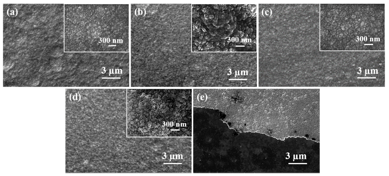
Figure 1 presents SEM images of carbon films deposited on stainless steel with Cr/CrSiVN interlayers with different V contents. As shown, the carbon films are all continuous and dense for samples with interlayers having vanadium contents ranging from 0 to 6.8 at.%. The grains of the films are very fine, typically in the range of 50–100 nm, in spite of a relatively larger size for samples V-1.8-D and V-6.8-D. Notably, the film for sample at 9.7 at.% V delaminated during cooling (see Figure 1e).
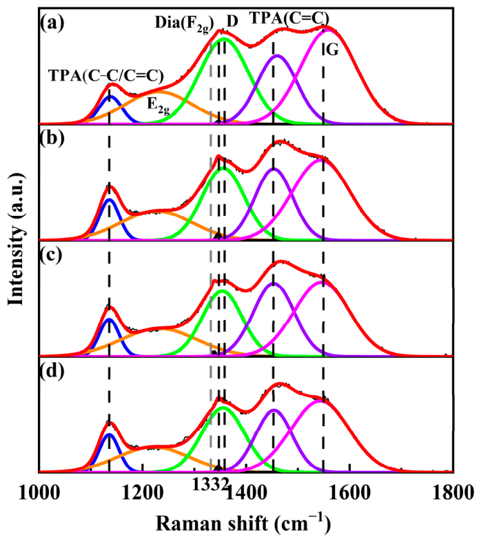
Figure 2 displays Raman spectra of diamond films deposited on stainless steel using Cr/CrSiVN interlayers with different V contents. Each Raman spectrum is deconvoluted into six Gaussian peaks by the least-squares method [21]. The peak at ~1332 cm−1 is assigned to the F2g vibrational mode of diamond [22,23]. The peaks at ~1350 cm−1 and ~1580 cm−1 are ascribed to the D band and G band of sp2 graphitic phases, respectively [24]. The peaks at ~1140 cm−1 and ~1470 cm−1 are attributed to the C-C/C=C and the C=C stretching vibrational modes of trans-polyacetylene (TPA) chains, respectively [24]. The peak at ~1200 cm−1 corresponds to the E2g vibrational mode of amorphous sp3 carbon [23]. The fitting results show that the diamond peak positions are 1344.5, 1343.3, 1343.6, and 1344.2 cm−1 for samples V-0-D, V-1.8-D, V-4.1-D, and V-6.8-D, respectively, indicating that the diamond films on the samples exhibit compressive residual stress. The stress in the diamond film is calculated by the following formula [21]:
σ = 0.567 ( ν d ν 0 )
where σ is the diamond stress, negative sign represents compressive stress, ν d and ν 0 are the position of the diamond characteristic peak and unstressed diamond peak (1332 cm−1), respectively. The calculated values are listed in Table 3. As shown, the stress in the diamond films is in the range of 6.4 to 7.1 GPa. The high stress is primarily attributed to thermal stress resulting from the large CTE difference between the steel substrate and the diamond film [25,26].
Moreover, the diamond content is calculated by formula [21]:
C D = I D I D + ( I C 233 ) × 100 %
where C D is the diamond content, I D is the peak area of the diamond peak, and I C is the sum of the peak area except for the diamond peak. The calculated diamond contents are also shown in Table 3. It is seen that the four samples exhibit comparable diamond contents of approximately 35%. In short, the V content in the interlayer does not significantly affect either the residual stress or the diamond content of the diamond film deposited on stainless steel.

3.2. Adhesion of the Diamond Film

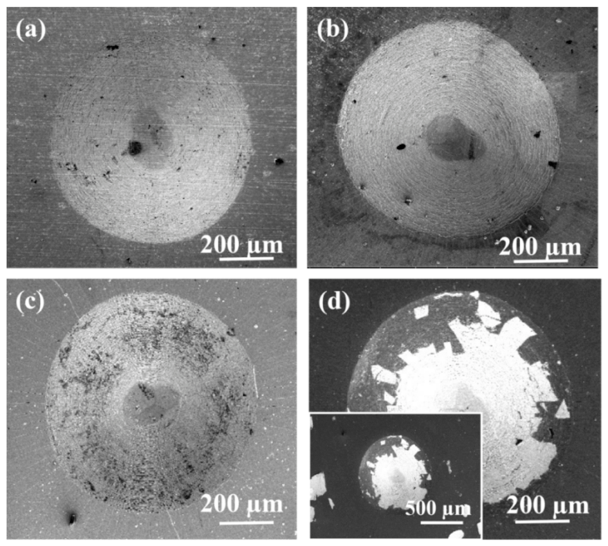
The adhesion of diamond films deposited on stainless steel with chromium nitride-based interlayer is generally excellent under static indentation testing but poor under scratch testing [27]. We used Rockwell C indentation testing and scratch testing to evaluate the adhesion of diamond films on stainless steel under static and scratch conditions, respectively. Figure 3 shows SEM images of the indentation imprint on all diamond films. No delamination around the imprint is observed for samples V-0-D, V-1.8-D, and V-4.1-D under a load of 150 kgf, indicating good adhesion of the diamond film at a V content of 0–4.1 at.% under static conditions. According to the VDI 3198 standard, the adhesion of these diamond films corresponds to grade HF1 [18]. However, extensive delamination of the diamond film was observed around the indentation crater for sample V-6.8-D (see the inset in Figure 3d), suggesting poor adhesion of the diamond film at a V content of 6.8 at.%. Considering that the diamond film delaminated on the sample V-9.7-D as described in Section 3.1, it is believed that the adhesion of diamond film under static conditions becomes poor at a V content larger than or equal to 6.8 at.%.
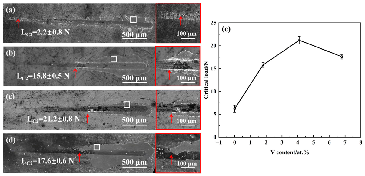
Figure 4 shows SEM images of the scratches on all diamond films. The critical load (Lc2) of the diamond film firstly rises from 2.2 ± 0.8 to 21.2 ± 0.8 N as the V content increases from 0 to 4.1 at.%, then it decreases to 17.6 ± 0.5 N as the V content reaches 6.8 at.%, suggesting that scratch adhesion can be improved by adding an appropriate amount of V to the interlayer. In addition, EDS analysis was performed on the delaminated areas (see white square in Figure 4). As shown in Table 4, there is a large amount of Cr and C elements and a small amount of Fe, Si, and V elements at the delamination site for all samples. It is believed that the failure occurs at the diamond/Cr-C interface in the scratch test considering that the stress concentration of the diamond film and that of the Cr-C interlayer are very different.

3.3. Analysis of the Reasons for Adhesion Improvement

The scratch adhesion of diamond film on stainless steel is influenced by multiple factors, including the residual stress and diamond content of the diamond film, the microstructure of the diamond/carbide layer interface (such as the type and thickness of the carbide layer, as well as the presence of pores at the interface) , and the hardness of the interlayer.
High residual stress typically leads to poor adhesion [28]. Films with a high diamond content exhibit high hardness, which enhances its resistance to plastic deformation and consequently improves adhesion in scratch tests [29]. As mentioned before, the stresses in diamond films with different V contents are comparable, and the diamond content is also similar for samples. Therefore, the improvement in adhesion with V addition cannot be ascribed to variations in stress or the diamond content of the film.
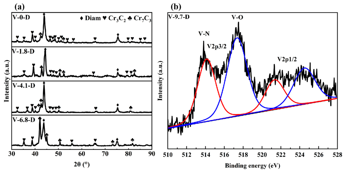
The type of carbide also affects the adhesion of the diamond film on stainless steel. A higher proportion of Cr3C2 generally leads to better adhesion, because the adhesion strength between diamond and Cr3C2 is greater than that between diamond and Cr7C3 [30]. As shown in Figure 5a, both Cr3C2 and Cr7C3 carbide phases exist in all samples. The ratio of the Cr3C2 peak area to the Cr7C3 peak area in the GIXRD pattern was calculated, representing the relative volumetric content of these chromium carbides in each sample. It is seen from Table 5 that the Cr3C2 content decreases as the V content in the interlayer increases. The V-0-D sample exhibits the highest content of Cr3C2 carbide phases (81.6 vol%) without the addition of V, while sample V-6.8-D has the lowest (22.1 vol%). Therefore, adhesion would be expected to decrease with increasing V content from 0 to 4.1 at.%. However, this is not the case, implying that other factors must be responsible.
The existence of vanadium carbides such as VC, V4C3, and V6C5 also can enhance adhesion strength [31,32]. However, XRD cannot detect carbide phases present at contents below about 5%, so their presence remains uncertain. Given that XPS is capable of identifying small amounts of carbides, we employed it to detect the existence of the carbide in the delaminated region of the sample. The V-9.7-D sample was chosen given that more vanadium carbide is likely to form when V content is high. Figure 5b shows the XPS spectra of the substances at the delaminated region for sample V-9.7-D. No V-C peak is observed at 512.6 eV, indicating that V atoms in the interlayer did not react with carbon atoms during the CVD process. The V2p3/2 peaks at 514.1 eV and 517.3 eV correspond to V-N and V-O bonds, respectively. The V-O peak is considered to be related to atmospheric contamination. The absence of vanadium carbide and the predominant formation of chromium carbide can be ascribed to the lower free energy of formation of chromium carbides (Cr7C3: −153.6 kJ/mol, Cr3C2: −791.0 kJ/mol) compared to vanadium carbides (VC0.73: −97.0 kJ/mol, VC: −102.1 kJ/mol, V2C: −146.4 kJ/mol) [33].
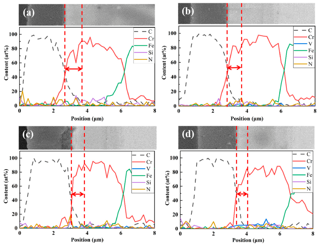
The thickness of the carbide layer also plays a role in the adhesion. Only a carbide layer above a certain critical thickness can ensure high adhesion. When the carbide layer is thinner than this critical value, the diamond film exhibits poor adhesion because it fails to provide sufficient bonding strength at the interface [34]. Figure 6 shows EDS line scanning for the samples with different V contents. It is observed that the carbide layer thicknesses are 0.9, 0.8, 0.7, and 0.6 μm for samples V-0-D, V-1.8-D, V-4.1-D, and V-6.8-D, respectively, indicating that the thickness decreases with increasing V content. The samples V-0-D, V-1.8-D, and V-4.1-D show good adhesion, whereas the adhesion of sample V-6.8-D becomes poor. Sufficient diamond film adhesion is only available when the carbonized interlayer carbide reaches a critical thickness. So, it is considered that the diamond film on the sample has lower adhesion due to a thinner carbide layer at a higher V content. Here, the reduced thickness of the carbide layer can be attributed to the slowing of carbon diffusion rate by the incorporation of V atoms, as mentioned above.
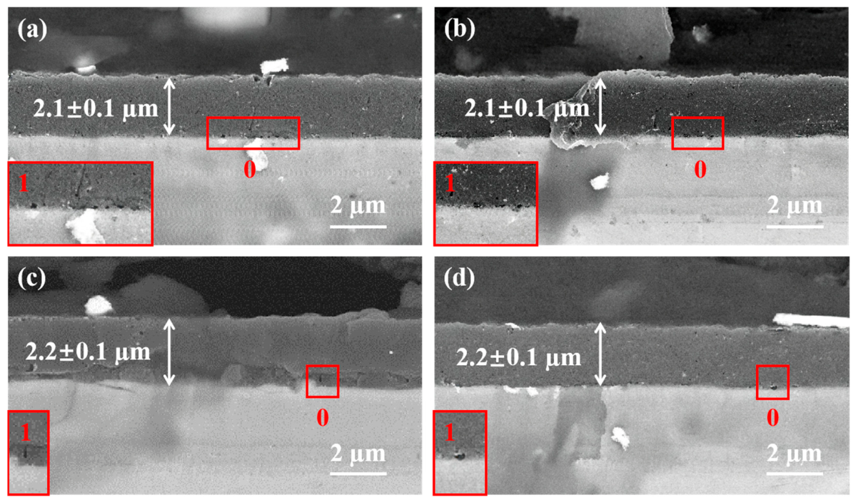
Additionally, it is reported that the defects or pores at the diamond/interlayer interface deteriorate the adhesion under scratch conditions [27]. Figure 7 shows cross-sectional images of the samples. It is observed that the carbon films’ thicknesses for samples V-0-D and V-1.8-D are all 2.1 μm, while those of samples V-4.1-D and V-6.8-D are slightly larger, at 2.2 μm. This suggests that the carbon film thickness is almost the same for all samples. The diamond/interlayer interface is flat in each sample. As shown in Figure 7, many pores with a size of 20–50 nm are visible at the interface for sample V-0-D. In contrast, the number of pores becomes small and the size of the pore remains nearly unchanged when a vanadium-incorporated interlayer is adopted. Three SEM fields were randomly selected for each sample, corresponding to a total interface length of ~30 μm. The interfacial porosity at the diamond/CrSiVN interface was determined by counting visible pores and normalized to the number of pores per 10 μm of interface length. The calculated values for samples V-0-D, V-1.8-D, V-4.1-D and V-6.8-D are 5, 3, 1, 1 pores/10 μm, respectively. This indicates the volume of pores at the diamond/interlayer interface decreases as more V is incorporated into the interlayer. The improved adhesion of the diamond films can also be ascribed to the reduction in porosity at the diamond/interlayer interface.
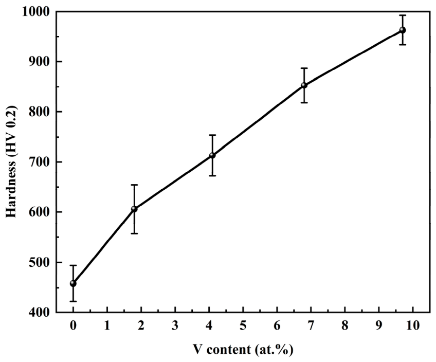
The hardness of the interlayer also influences the adhesion of the diamond film [35,36]. A high-hardness interlayer beneath the diamond film reduces the difference in plastic deformation between the diamond film and the interlayer under load, leading to a higher critical failure force during scratching. Figure 8 shows the hardness of the sample with CrSiVN interlayer with different V contents. It rises progressively from 458.1 ± 35.9 to 963.2 ± 29.6 HV 0.2 as the V content increases from 0 to 9.7 at.%. Therefore, it is believed that the improvement in diamond film adhesion under scratching conditions is partially attributed to the increase in the hardness of the interlayer.
In all, the enhanced adhesion of diamond film on the stainless steel using CrSiVN interlayer is caused by formation of a carbide layer with a thickness larger than a critical value, reduced porosity at the diamond/interlayer interface, and increased hardness of interlayer, rather than residual stress, diamond content, or carbide type.
In order to understand the effect of CrSiN interlayer with V incorporation on the thickness of carbide layer, the porosity at the interface, and the effect of V content on the interlayer hardness, we used GIXRD and SEM to characterize the phase composition and grain size of the interlayer with different V contents, respectively.
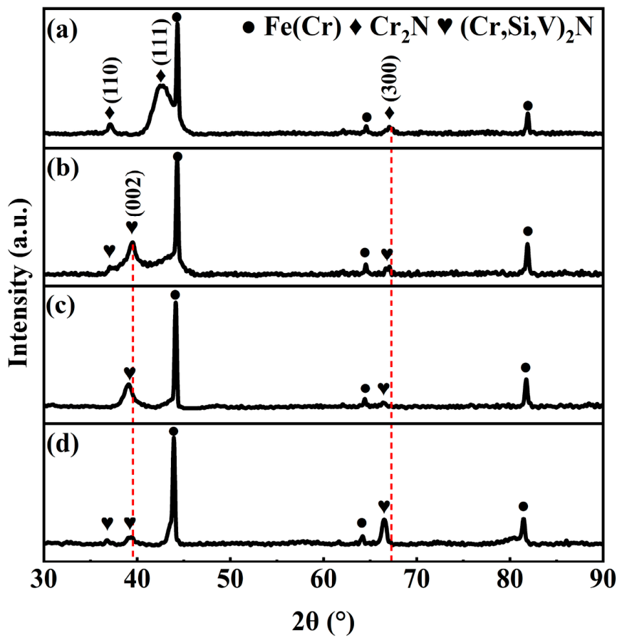
Figure 9 shows the GIXRD patterns of the interlayer with different V contents. It is observed that when V is not added to the interlayer, there are three peaks at 37.4°, 42.7°, and 67.5°, which correspond to crystal planes (110), (111), and (300) of Cr2N from the JCPDF card (No. 35-0803). This suggests that the interlayer mainly consists of (Cr,Si)2N phase, which is in agreement with our previous result [21]. The peaks attributed to crystal planes (002) and (300) all shift to a low angle with increasing V content from 1.8 to 6.8 at.%. This peak shift is attributed to the substitution of Cr atoms (radius: 128 pm) by larger V atoms (radius: 134 pm). The disappearance of the peak at 42.7° corresponding to crystal plane (111) after V incorporation is related to the grain orientation. It is considered that the interlayer is also mainly composed of (Cr,Si,V)2N solid solution after V incorporation. Additionally, the full width at half maximum (FWHM) of the peak attributed to crystal planes (111) and (300) is very large for sample V-0, suggesting the poor crystallinity of (Cr,Si)2N in the absence of V. Compared to the FWHM of the peak attributed to crystal plane (300) (0.757°) for sample V-0, the FWHM of the crystal plane (300) becomes small after V addition and is 0.470°, 0.515°, and 0.554° for V contents of 1.8, 4.1 and 6.8 at.%, respectively. This indicates that crystallinity of the interlayer is improved after V addition and lattice distortion intensifies with increasing V content. This is believed to be associated with the higher bond energy of the V-N bond (523 ± 38 kJ/mol) than that of the Cr-N bond (377.8 ± 18.8 kJ/mol) [37]. In all, the interlayer after V addition is mainly composed of (Cr,Si,V)2N solid solution with better crystallinity.
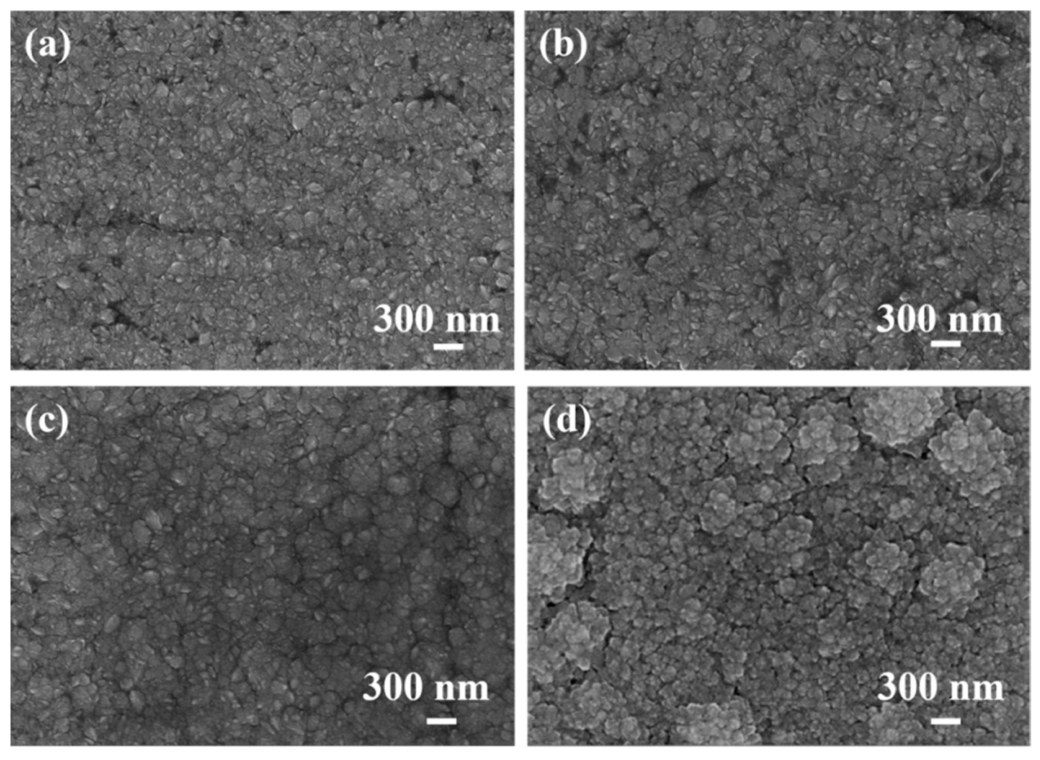
As shown in Figure 10, samples V-0, V-1.8, and V-4.1 are composed of grains with a size ranging from 100 to 150 nm. In sample V-6.8, the grain size also ranges from 100 to 150 nm, although some large cluster-like particles are also observed. In summary, the grain size of the interlayers is similar at different V contents.
Thus, the reduction in carbide layer thickness and porosity at the interface with the increase in V content in the interlayer can be explained as follows. Generally, the formation of Cr–C compounds consists of three steps: adsorption of carbon atoms on the CrSiVN interlayer, cleavage of M–N (M = Cr, V, Si) bonds, and subsequent generation of chromium carbides via Cr–C bond generation. The melting point of VN is 2360 °C, whereas that of Cr2N is only 1650 °C [38], which indicates that the V–N bond possesses higher bonding energy than the Cr–N bond. Doping V into CrSiN films causes V atoms to replace Cr lattice sites. Higher V doping concentrations boost the average M–N bonding energy, hindering M–N bond breakage and carbide formation, and resulting in a thinner carbide interlayer. It is reported that the carbide is porous when the extent of carburization is large; conversely, the carbide is dense under conditions of limited carbon incorporation [27]. Therefore, pores at the interface decrease due to the decrease in carbonization extent using the interlayer at high V content. In regard to increased hardness of Cr/CrSiVN interlayer, this is attributed to solid–solution strengthening by the substitution of Cr atoms by V atoms with larger radius.

3.4. A Simple Model

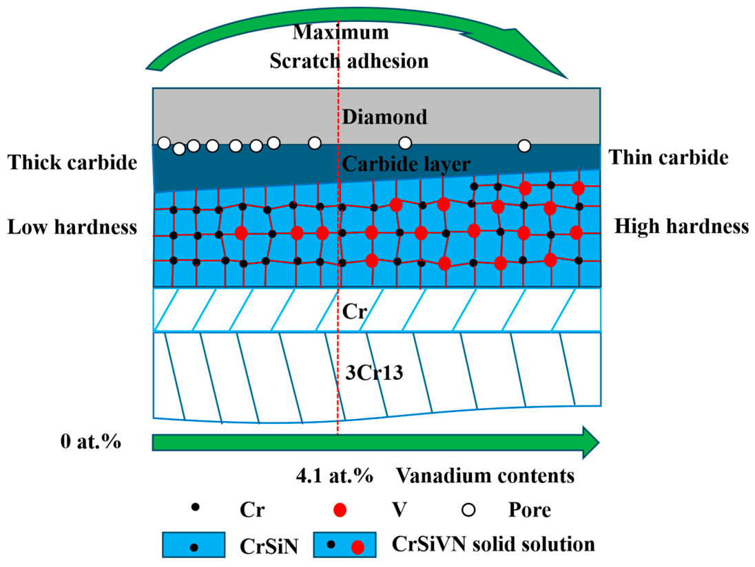
In summary, the effect of V content in the Cr/CrSiVN interlayer on the preparation of diamond films on stainless steel is summarized in Figure 11. As shown in the figure, with increasing V content in the interlayer, more V atoms dissolve into (Cr,Si)2N grains. This reduces the diffusion of C atoms during CVD deposition, leading to carbon supersaturation on the surface, which promotes rapid diamond nucleation. And the carburization degree of the interlayer is reduced, resulting in a thinner carbide layer and fewer pores at the diamond/carbide interface. The reduced porosity at the interface decreases stress concentration, thereby improving the adhesion of the diamond film. Moreover, the solid solution of V atoms in (Cr,Si)2N grains increases the hardness of the interlayer, which also enhances adhesion, as a harder interlayer provides better support for the diamond film, minimizing plastic deformation under load and reducing the risk of film delamination. As a result, the adhesion under scratching conditions increases with V content increasing from 0 to 4.1 at.%. The subsequent decrease in the adhesion is ascribed to the excessively thin carbide layer, because it cannot provide enough interfacial bonding.

4. Conclusions

In this work, Cr/CrSiVN interlayers with different V contents were utilized to deposit diamond films on stainless steel to improve adhesion under scratching condition. The conclusions are as follows: the interlayer effectively improves the adhesion of diamond films on stainless steel. The adhesion improves with V content of the interlayer increasing from 0 to 4.1 at.%, then follows a decrease at higher V content. The critical load achieves a maximum value of 21.2 ± 0.5 N at 4.1 at.%. The improvement in adhesion is attributed not to the residual stress or diamond content of the diamond film, nor to the type of underlying carbide, but to the following factors: (1) Optimized thickness of the carbide layer; (2) Reduced pore density at the diamond/carbide interface, which lowers stress concentration; (3) Enhanced hardness of the interlayer due to solid–solution strengthening. The carbide layer thickness decreases with increasing V content, and the minimum thickness required for high adhesion is 0.6–0.7 μm. The addition of V to the interlayer also reduces the diffusion rate of carbon atoms, leading to a thinner carbide layer and lower porosity at the interface. This study presents a novel interlayer that enables the deposition of adherent diamond films on stainless steel under scratch conditions, paving the way for potential applications in medical or food-processing equipment.

Author Contributions

Formal analysis, X.L. and J.Z.; Investigation, J.Z.; Data curation, X.Z., X.W. and J.Z.; Writing—original draft , J.Z. and X.W; Conceptualization, X.L. All authors have read and agreed to the published version of the manuscript.

Funding

This research was funded by the Key Project of National Natural Science Foundation of China (Grant No. U1809210), the International Science Technology Cooperation Program of China (2014DFR51160), Natural Science Foundation of Zhejiang Province (LQ15A040004), Open Project of State Key Laboratory of Superhard Materials, Jilin University (202011), the One Belt and One Road International Cooperation Project from Key Research and Development Program of Zhejiang Province (No. 2018C04021), the National Natural Science Foundation of China (Grant Nos. 11504325, 50972129, 50602039, 52002351, and 52102052), research projects from Institute of Wenzhou, Zhejiang University (Nos. XMGL-CX-202305 and XMGL-KJZX-202307), and the project from Tanghe Scientific & Technology Company (No. KYY-HX-20230024).

Institutional Review Board Statement

Not applicable.

Informed Consent Statement

Not applicable.

Data Availability Statement

All relevant data are within the paper.

Conflicts of Interest

The authors declare that they have no known competing financial interests or personal relationships that could have appeared to influence the work reported in this paper.

References

  1. Huang, K.; Hu, X.J.; Xu, H.; Shen, Y.G.; Khomich, A. The oxidization behavior and mechanical properties of ultrananocrystalline diamond films at high temperature annealing. Appl. Surf. Sci. 2014, 317, 11–18. [Google Scholar] [CrossRef]
  2. Li, X.; He, L.; Li, Y.; Yang, Q. Diamond Deposition on Iron and Steel Substrates: A Review. Micromachines 2020, 11, 719. [Google Scholar] [CrossRef] [PubMed]
  3. Buijnsters, J.G.; Shankar, P.; Ter Meulen, J. Direct deposition of polycrystalline diamond onto steel substrates. Surf. Coat. Technol. 2007, 201, 8955–8960. [Google Scholar] [CrossRef]
  4. Neto, V.F.; Shokuhfar, T.; Oliveira, M.S.A.; Gracio, J.; Ali, N. Polycrystalline diamond coatings on steel substrates. Int. J. Nanomanuf. 2008, 2, 99–115. [Google Scholar] [CrossRef]
  5. Handschuh-Wang, S.; Liu, X.; He, B.; Han, P.; Jiang, X.; Wang, T. Interfacial Engineering for Enhanced Adhesion of Diamond Coatings. Small 2026, 22, e12566. [Google Scholar] [CrossRef] [PubMed]
  6. Fan, Q.H.; Grácio, J.; Pereira, E.; Ali, N.; Ahmed, W. Study of diamond adhesion behavior on chromium and titanium for obtaining adherent diamond coatings on steel. J. Mater. Res. 2000, 15, 2330–2335. [Google Scholar] [CrossRef]
  7. Li, C.P.; Dai, W.; Li, M.J.; Li, H.J.; Xu, S.; Wu, X.G.; Yang, B.H. Effect of sputtered titanium interlayers on the properties of nanocrystalline diamond films. J. Appl. Phys. 2016, 119, 135306. [Google Scholar] [CrossRef]
  8. Li, Y.S.; Tang, Y.; Yang, Q.; Xiao, C.; Hirose, A. Diamond deposition on steel substrates with an Al interlayer. Int. J. Refract. Met. Hard Mater. 2009, 27, 417–420. [Google Scholar] [CrossRef]
  9. Buijnsters, J.G.; Vázquez, L.; Escobar Galindo, R.; Meulen, J. Molybdenum Interlayers for Nucleation Enhancement in Diamond CVD Growth. J. Nanosci. Nanotechnol. 2010, 10, 2885–2891. [Google Scholar] [CrossRef] [PubMed]
  10. Kundrát, V.; Zhang, X.L.; Cooke, K.; Sun, H.L.; Sullivan, J.; Ye, H.T. A novel Mo-W interlayer approach for CVD diamond deposition on steel. AIP Adv. 2015, 5, 047130. [Google Scholar] [CrossRef]
  11. Kundrát, V.; Zhang, R.Y.; Zhang, X.L.; Cooke, K.; Sun, H.L.; Sullivan, J.; Ye, H.T. The effect of MoW interlayer thickness on diamond growth on steel substrates. J. Mater. Res. 2020, 35, 491–499. [Google Scholar] [CrossRef]
  12. Polini, R.; Barletta, M. On the use of CrN/Cr and CrN interlayers in hot filament chemical vapour deposition (HF-CVD) of diamond films onto WC-Co substrates. Diam. Relat. Mater. 2008, 17, 325–335. [Google Scholar] [CrossRef]
  13. Sun, X.Y.; Li, Y.S.; Wan, B.Q.; Yang, L.Z.; Yang, Q.Q. Deposition of diamond coatings on Fe-based substrates with Al and Al/AlN interlayers. Surf. Coat. Technol. 2015, 284, 139–144. [Google Scholar] [CrossRef]
  14. Li, X.; Shan, Y.L.; Xia, F.; Chen, C.K.; Lu, S.H.; Hu, X.J. Preparation of Diamond Films with Cracked Textures on Stainless Steel Using W/W-N Film as an Interlayer. Coatings 2024, 14, 1494. [Google Scholar] [CrossRef]
  15. Lyu, F.; Li, X.; Chen, C.K.; Liu, C.; Li, C.X.; Jiang, M.Y.; Hu, X.J. High adhesion diamond films deposited on stainless steel by using nanocomposite films with mosaic interface as an interlayer. Appl. Surf. Sci. 2020, 528, 146916. [Google Scholar] [CrossRef]
  16. Damm, D.D.; Contin, A.; Barbieri, F.C.; Trava-Airoldi, V.J.; Barquete, D.M.; Corat, E.J.; Buijnsters, I. Interlayers Applied to CVD Diamond Deposition on Steel Substrate: A Review. Coatings 2017, 7, 141. [Google Scholar] [CrossRef]
  17. Xu, B.B.; Guo, P.; Wang, Z.Y.; Chen, R.D.; Ye, Y.M.; Shuai, J.T.; Wang, A.Y.; Ke, P.L. Anti-wear Cr-V-N coating via V solid solution: Microstructure, mechanical and tribological properties. Surf. Coat. Technol. 2022, 397, 126048. [Google Scholar] [CrossRef]
  18. Vidakis, N.; Antoniadis, A.; Bilalis, N. The VDI 3198 indentation test evaluation of a reliable qualitative control for layered compounds. J. Mater. Process. Technol. 2003, 143–144, 481–485. [Google Scholar] [CrossRef]
  19. Li, J.; Beres, W. Scratch Test for Coating/Substrate Systems—A Literature Review. Can. Metall. Q. 2007, 46, 155–173. [Google Scholar] [CrossRef]
  20. Steinmann, P.A.; Tardy, Y.; Hintermann, H.E. Adhesion testing by the scratch test method: The influence of intrinsic and extrinsic parameters on the critical load. Thin Solid Films 1987, 154, 333–349. [Google Scholar] [CrossRef]
  21. Li, X.; Wang, C.C.; Chen, C.K.; Jiang, M.Y.; Hu, X.J. Thickness-controllable diamond films deposited on stainless steel using a Cr/Cr-Si-N interlayer prepared at different N2/Ar flow ratios. Appl. Surf. Sci. 2020, 532, 147402. [Google Scholar] [CrossRef]
  22. Pu, M.; Zhang, F.; Liu, S.; Irifune, T.; Lei, L. Tensile-strain induced phonon splitting in diamond. Chin. Phys. B 2019, 28, 053102. [Google Scholar] [CrossRef]
  23. El Mendili, Y.; Orberger, B.; Chateigner, D.; Bardeau, J.-F.; Gascoin, S.; Petit, S. Raman investigations and ab initio calculations of natural diamond-lonsdaleite originating from New Caledonia. Chem. Phys. 2022, 559, 111541. [Google Scholar] [CrossRef]
  24. Chen, C.; Mei, Y.; Cui, J.; Li, X.; Jiang, M.; Lu, S.; Hu, X. Man-made synthesis of ultrafine photoluminescent nanodiamonds containing less than three silicon-vacancy colour centres. Carbon 2018, 139, 982–988. [Google Scholar] [CrossRef]
  25. Damm, D.D.; Volu, R.M.; Correia, R.F.B.O.; Almeida, K.F.; Trava-Airoldi, V.J.; de Vasconcelos, G.; Barquete, D.M.; Corat, E.J. A Novel Method to Deposit Vanadium Carbide Interlayer on Tool Steel Substrate Applied to Mitigate CVD Diamond Thermal Stresses. Metall. Mater. Trans. A 2024, 55, 3478–3491. [Google Scholar] [CrossRef]
  26. Martins, R.L.; Damm, D.D.; Corat, E.J.; Trava-Airoldi, V.J.; Barquete, D.M. Mitigating residual stress of high temperature CVD diamond films on vanadium carbide coated steel. J. Vac. Sci. Technol. A 2020, 39, 013401. [Google Scholar] [CrossRef]
  27. Li, X.; Chen, H.; Wang, C.C.; Chen, C.K.; Jiang, M.Y.; Hu, X.J. Improvement of adhesion under the scratching condition for diamond film on the steel by adding a precarbonization process. Diam. Relat. Mater. 2023, 136, 109927. [Google Scholar] [CrossRef]
  28. Li, Y.S.; Tang, Y.; Yang, Q.; Xiao, C.; Hirose, A. Growth and adhesion failure of diamond thin films deposited on stainless steel with ultra-thin dual metal interlayers. Appl. Surf. Sci. 2010, 256, 7653–7657. [Google Scholar] [CrossRef]
  29. Li, X.; Xia, F.; Wang, C.C.; Chen, C.K.; Jiang, M.Y.; Pan, J.P.; Lu, S.H.; Khomich, A.A.; Vlasov, I.; Hu, X.J. Deposition of an adherent diamond film on stainless steel using Cr/CrAlN as an interlayer. Surf. Coat. Technol. 2022, 449, 128960. [Google Scholar] [CrossRef]
  30. Kellermann, K.; Bareiß, C.; Rosiwal, S.M.; Singer, R.F. Well Adherent Diamond Coatings on Steel Substrates. Adv. Eng. Mater. 2008, 10, 657–660. [Google Scholar] [CrossRef]
  31. Damm, D.D.; Contin, A.; Gomes, M.C.C.B.; Trava-Airoldi, V.J.; Barquete, D.M.; Corat, E.J. Adherent HFCVD diamond on steels substrates using vanadium carbide intermediate layer. Diam. Relat. Mater. 2018, 89, 218–226. [Google Scholar] [CrossRef]
  32. Damm, D.D.; Contin, A.; Trava-Airoldi, V.J.; de Vasconcelos, G.; Barquete, D.M.; Corat, E.J. Synthesis of Vanadium Interface for HFCVD Diamond Deposition on Steel Surface. Mater. Res. 2017, 20, 248–253. [Google Scholar] [CrossRef]
  33. Anthonysamy, S.; Ananthasivan, K.; Kaliappan, I.; Chandramouli, V.; Vasudeva Rao, P.R.; Mathews, C.K.; Jacob, K.T. Gibbs energies of formation of chromium carbides. Metall. Mater. Trans. A 1996, 27, 1919–1924. [Google Scholar] [CrossRef]
  34. Fischer, M.; Chandran, M.; Akhvlediani, R.; Hoffman, A. Interplay between adhesion and interfacial properties of diamond films deposited on WC-10%Co substrates using a CrN interlayer. Diam. Relat. Mater. 2016, 70, 167–172. [Google Scholar] [CrossRef]
  35. Zhang, C.D.; Hu, T.; Zhang, N. Influence of Substrate Hardness on Coating-Substrate Adhesion. Adv. Mater. Res. 2010, 177, 148–150. [Google Scholar] [CrossRef]
  36. Ghio, E.; Bolelli, G.; Bertè, A.; Cerri, E. Diamond-Like Carbon (DLC) and AlCrN films onto Ti-6Al-4V substrates by Laser-Powder Bed Fusion (L-PBF): Effect of substrate heat treatment and surface finish. Surf. Coat. Technol. 2023, 475, 130128. [Google Scholar] [CrossRef]
  37. Hanes, W.M. Handbook of Chemistry and Physics, 97th ed.; CRC Press: New York, NY, USA, 2016; p. 9-75–9-76. [Google Scholar]
  38. Yuan, Z.Z.; Dai, Q.X. Metallic Materials, 3rd ed.; Chemical Industry Press: Beijing, China, 2008; p. 18. [Google Scholar]
Figure 1. SEM images of diamond films prepared on stainless steel using Cr/CrSiVN interlayer with different V contents: (a) 0 at.%, (b) 1.8 at.%, (c) 4.1 at.%, (d) 6.8 at.%, and (e) 9.7 at.%.
Coatings 16 00908 g001
Figure 2. Raman spectra of diamond films prepared on stainless steel using Cr/CrSiVN interlayer with different V contents: (a) 0 at.%, (b) 1.8 at.%, (c) 4.1 at.%, and (d) 6.8 at.%.
Coatings 16 00908 g002
Figure 3. SEM images of the imprint of diamond film prepared on stainless steel using Cr/CrSiVN interlayer with different V contents: (a) 0 at.%, (b) 1.8 at.%, (c) 4.1 at.%, and (d) 6.8 at.%. The inset is the reduced image of the indentation imprint for the sample.
Coatings 16 00908 g003
Figure 4. SEM images of diamond films prepared on stainless steel using Cr/CrSiVN interlayers with different V contents after the scratch test: (a) 0 at.%, (b) 1.8 at.%, (c) 4.1 at.%, and (d) 6.8 at.%. (e) Plot of critical load versus vanadium concentration. The insets in figures (ad) are the enlarged views of failure regions at the critical load. The red arrows indicate the initial delamination areas of the film.
Coatings 16 00908 g004
Figure 5. (a) GIXRD patterns of diamond films prepared on stainless steel using Cr/CrSiVN interlayers with different V contents and (b) XPS spectrum of substances in the delamination area of the diamond film sample (V-9.7-D).
Coatings 16 00908 g005
Figure 6. EDS line scan of diamond films prepared on stainless steel using Cr/CrSiVN interlayers with different V contents: (a) 0 at.%, (b) 1.8 at.%, (c) 4.1 at.%, and (d) 6.8 at.%. The arrows between the two dashed lines denote the thickness of the carbide layer.
Coatings 16 00908 g006
Figure 7. SEM images of cross-section of samples using Cr/CrSiVN interlayer with different V contents: (a) 0 at.%, (b) 1.8 at.%, (c) 4.1 at.%, and (d) 6.8 at.%. The inset “1” is the magnified image of region “0”.
Coatings 16 00908 g007
Figure 8. Vickers hardness of Cr/CrSiVN interlayers with different V contents.
Coatings 16 00908 g008
Figure 9. GIXRD patterns of Cr/CrSiVN interlayers with different V contents: (a) 0 at.%, (b) 1.8 at.%, (c) 4.1 at.%, and (d) 6.8 at.%. Red dashed lines indicate the peak of Cr2N.
Coatings 16 00908 g009
Figure 10. Surface morphology of Cr/CrSiVN interlayers with different V contents: (a) 0 at.%, (b) 1.8 at.%, (c) 4.1 at.%, and (d) 6.8 at.%.
Coatings 16 00908 g010
Figure 11. Role of V content in CrSiVN interlayer on preparation of diamond film on stainless steel. The red dashed line indicates the maximum scratch adhesion at 4.1 at.% V content.
Coatings 16 00908 g011
Table 1. Deposition parameters of Cr/CrSiVN interlayer.
Cr LayerCrSiVN Layer
Flux of N2/Ar (sccm)0/205/20
Base pressure (Pa)3 × 10⁻³
Working pressure (Pa)0.8
Substrate temperature (°C)300
Bias voltage (V)−100
Power of Cr (W)200
Power of Si (W)060
Power of V (W)00/30/60/90/120
Deposition time (min)2060
Rotation rate of substrate (r/min)4
Table 2. Deposition parameters of diamond film.
First StepSecond Step
Deposition power (W)18001600
Deposition time (min)2050
Substrate temperature (°C)830750
Bias current (A)4
Working pressure (kPa)1.38
Flux of H2 (sccm)200
Flux of acetone (sccm)80
Distance between substrate and wire (mm)18
Rotation rate of substrate (r/min)20
Table 3. Diamond peak position, residual stress, and diamond content of diamond film prepared on stainless steel using Cr/CrSiVN interlayers with different V contents.
SampleDiamond Peak Position (cm−1)Residual Stress (GPa)Diamond Content (%)
V-0-D1344.5−7.135.0
V-1.8-D1343.3−6.433.2
V-4.1-D1343.6−6.630.8
V-6.8-D1344.2−6.935.7
Table 4. Composition of delaminated regions of samples with different V contents after the scratch test.
SampleElement Content (at.%)
CCrSiVNFe
V-0-D54.141.41.20.00.01.2
V-1.8-D49.746.80.71.60.01.1
V-4.1-D46.848.10.92.90.00.9
V-6.8-D48.245.70.53.80.01.8
Table 5. Peak area of chromium carbide of Cr3C2 and Cr7C3 in GIXRD.
SamplePeak Area of Cr3C2 (S1)Peak Area of Cr7C3 (S2)S1/(S1 + S2)
V-0-D38,178863281.6%
V-1.8-D3550273956.4%
V-4.1-D4605507747.6%
V-6.8-D1793630222.1%
Disclaimer/Publisher’s Note: The statements, opinions and data contained in all publications are solely those of the individual author(s) and contributor(s) and not of MDPI and/or the editor(s). MDPI and/or the editor(s) disclaim responsibility for any injury to people or property resulting from any ideas, methods, instructions or products referred to in the content.