1. Introduction
Diamond-like carbon (DLC) films have been widely used because of their excellent lubrication properties and biocompatibility [
1,
2]. However, the pristine DLC film exhibits high electrical resistivity, large internal stress and poor thermal stability [
3], and these drawbacks can be alleviated by metal doping [
4,
5]. In addition, it has recently been discovered that the DLC film has a piezoresistive effect [
6,
7,
8]. This makes it an attractive material for manufacturing advanced sensors [
9,
10,
11].
The piezoresistive properties of the DLC films with the addition of elements including W [
12,
13], Cr [
14], Ag [
15,
16], Sn [
17], Ni [
18,
19,
20,
21], Ti [
22], Cu [
23,
24], and Nb [
25] have been reported. Takeno et al. [
13] used plasma-enhanced chemical vapor deposition and DC magnetron co-sputtering to prepare DLC:W films. They found a linear relationship between the resistance change rate of the films and the tensile or compressive strains in the range of 0–600 MPa, exhibiting a gauge factor of 6.1. Gudaitis et al. [
14] prepared DLC:Cr films using RF diode sputtering technology. The gauge factor of the films was proportional to the sp
3/sp
2 ratio of the film. Tamulevičius et al. [
16] studied the effects of varying deposition conditions (such as bias voltage, gas flow ratio, etc.) on chemical composition, microstructure, and piezoresistive properties of the DLC films containing Ag by plasma-assisted deposition. The results show that the gauge factor of the DLC:Ag film decreases with the increase in the Ag concentrations, while it increases with the rise in the sp
3/sp
2 ratio. Leal et al. [
17] prepared DLC:Sn films using a dual magnetron sputtering system. The results show that there are more large Sn clusters in high-power pulsed magnetron sputtering (HiPIMS) thin films than in those deposited by the DC power supply. The lower resistivity of the HiPIMS thin films may be related to the large Sn clusters and the increased amounts of sp
2 bonds in the DLC:Sn films. The electrical resistance of the DLC:Sn film decreases linearly as the applied mass increases from 0 to 600 g. Koppert et al. [
18] studied the structure and piezoresistive properties of the DLC:Ni films prepared by reactive sputtering. The gauge factor reached ~20. It was found that single-crystal Ni clusters with diameters of 10~20 nm were surrounded by carbon shells. Petersen et al. [
22] prepared DLC:Me films by the DC sputtering method. They found that Ti and W favor forming carbides, and the gauge factor of the films was 1~2. Meškinis et al. [
23] reported that the Cu-containing DLC (DLC:Cu) films fabricated by reactive magnetron sputtering exhibit gauge factors of 3~6. The gauge factors decrease with increasing concentration of copper atoms. Grein et al. [
25] prepared Nb-containing DLC by the HiPIMS process. The results show that the thin films have a high gauge factor of 35.5, and they are suitable as sensor materials for strain gauges. Zhang et al. [
26] synthesized a series of Cr-DLC nanocomposite films with varying chromium content using HiPIMS. The film with an optimal Cr concentration achieved a gauge factor of approximately 22.8. The authors systematically investigated the effects of Cr content on the film structure, composition, electrical properties, and energy band structure, and explored the underlying carrier transport and piezoresistive mechanisms. Koppert et al. [
21] reported that a DLC film with a Ni content of 52 at.% exhibited a gauge factor of 14 and a near-zero temperature coefficient of resistance (TCR) over the temperature range of 90–400 K. Meškinis et al. [
23] proposed a percolation-tunneling model, while Tibrewala et al. [
8] put forward a thick film resistor (TFR) model, suggesting that applied strain can alter the carrier transport pathways. The mechanism for regulating the piezoresistive coefficient of metal-doped DLC is primarily related to the carbon structure of the DLC. Doping metals such as Ti and Cr prefer to form Me–C bonds, leading to an increase in the sp
2 content and promoting graphitization of the films. In addition, Yan et al. [
24] confirmed the occurrence of both thermal activation transport and three-dimensional Mott-type variable range hopping (VRH) conduction under varying temperatures. They explained the electrical properties and piezoresistive effects in Cu-DLC through carrier tunneling processes between the conductive phases within the insulating sp
3 matrix.
The above investigations focus on the evolution of the sp
3/sp
2 ratio and its impact on the piezoresistive properties. Few studies have focused on how external loading alters the chemical bonding and phase composition of metal-doped DLC films, as well as the corresponding cyclic stability of their piezoresistive performance. In addition, the distinct bonding characteristics between different metal and carbon atoms can significantly alter the bond structure and electronic states of the films [
27,
28,
29]. Therefore, the incorporated metal atoms can either dissolve atomically or aggregate into nanoscale metal/carbide particles within the DLC matrix, depending on their concentration, leading to diverse microstructures and carrier behavior [
29]. In addition, the structural evolution of carbon networks is critical for sensor applications but is rarely discussed in reported piezoresistive models. Consequently, a mechanistic understanding of the evolution of these films’ piezoresistive characteristics remains unknown [
30]. Therefore, this work fabricated the DLC films with varying Ti concentrations. The effects of varying Ti concentrations on microstructure, chemical bonding structure, and piezoresistive performance of the DLC films were investigated. The mechanism behind the evolution of piezoresistive performance was discussed as well.
2. Materials and Methods
Si3N4 substrates (Dongguan Xiayang New Materials Co., Ltd., Dongguan, China, 20 × 20 × 2 mm) and polycrystalline Si wafers were used as the substrates for the film deposition. The Si3N4 substrates were first ground with sandpaper and then polished with 2.5 μm diamond powder. Subsequently, the substrates were ultrasonically cleaned in deionized water for 30 min and ethanol for 25 min. The deposition was carried out in a DG-3BY coating system (Liaoning Beiyu Vacuum Technology Co., Ltd., Tieling, China). The vacuum system consisted of a turbomolecular pump backed by an oil-sealed rotary vane pump. Plasma etching was conducted using an anode-layer ion source (ALS) in an Ar atmosphere with a gas flow rate of 200 sccm for 20 min. The Ar gas (99.999% purity) with a flow rate of 180 sccm and the C2H2 gas (99.999% purity) with a flow rate of 20 sccm were introduced into the vacuum chamber for film deposition. The working pressure was maintained at 0.4 Pa. The substrate bias was fixed at −100 V. There was no external substrate heating, and the working distance was 15 cm. Diamond-like carbon (DLC) films were deposited using a direct current magnetron sputtering (DCMS) with Ti sputtering power ranging from 1300 to 1700 W. The Ti target (Beijing Tianqi Advanced Materials Co., Ltd., Beijing, China, purity 99.99%, size 470 × 110 × 8 mm) was connected to a DC power supply and pre-sputtered for 15 min.
Film thickness and morphology were characterized via cross-sectional scanning electron microscopy (SEM) using a LEO 1550 scanning electron microscope (Oberkochen, Germany). SEM observations were conducted at an accelerating voltage of 15 kV and a working distance of 4 mm with a secondary electron (SE) detector. The film crystal structure was studied using a PANalytical (Almelo, The Netherlands) X’Pert PRO X-ray diffractometer operated with Cu K
α radiation (0.154 nm wavelength). The X-ray tube was operated at a voltage of 40 kV and a current of 40 mA. Grazing incidence X-ray diffraction (GIXRD) patterns were recorded with an incident angle of 1°, a step size of 0.02°, a step time of 0.1 s, and a scanning range of 30–70°. X-ray photoelectron spectroscopy (XPS) spectra were acquired in a Kratos analytical (Manchester, UK) instrument, with a base pressure of 1.1 × 10
−9 Torr (1.5 × 10
−7 Pa), using monochromatic Al K
α radiation (
hγ = 1486.6 eV) with the X-ray anode operated at 150 W. All core-level spectra are referenced to the Fermi level cutoff, which defines zero binding energy (BE) [
31,
32]. Before XPS analyses, the film surfaces were sputter-cleaned with 4 keV Ar
+ ions incident at 70° with respect to the surface normal for 2 min. The ion energy is then reduced to 0.5 keV for 10 min to minimize sputter damage [
33,
34]. After sputtering, all core-level spectra were acquired. Survey spectra were recorded with a pass energy of 150 eV and a step size of 1 eV. High-resolution core-level spectra were obtained with a pass energy of 50 eV and a step size of 0.05 eV, and multiple scans were collected to improve the signal-to-noise ratio. Binding energy was calibrated against the adventitious C 1s peak at 284.8 eV. The cross-sectional specimen was prepared using a focused ion beam (FIB, LYRA 3 XMU, Tescan, Brno, Czech Republic). Transmission electron microscopy (TEM, Talos F200S, Thermo Fisher Scientific, Waltham, MA, USA) observations were performed at an accelerating voltage of 200 kV, and the SAED patterns were acquired with a camera length of 50 cm.
The hardness and elastic modulus of the samples were measured using an Anton Paar TTX-NHT
2 nanoindenter (Anton Paar, Graz, Austria). The maximum load was fixed at 5 mN, with constant loading and unloading rates of 10 mN/min. The hardness and elastic modulus of the films were derived from the load–displacement curves using the Oliver–Pharr method. The electrical resistance of the samples was measured using a resistance tester (Rek RK2514, Shenzhen, China). The stress σ used in the test varied in the range of 0–35 MPa. The piezoresistive coefficient
KP was calculated based on the following Formula (1),
where
R is the resistance of the piezoresistive layer, Δ
R is the resistance change caused by strain, and
σ is the stress applied to the films.
3. Results
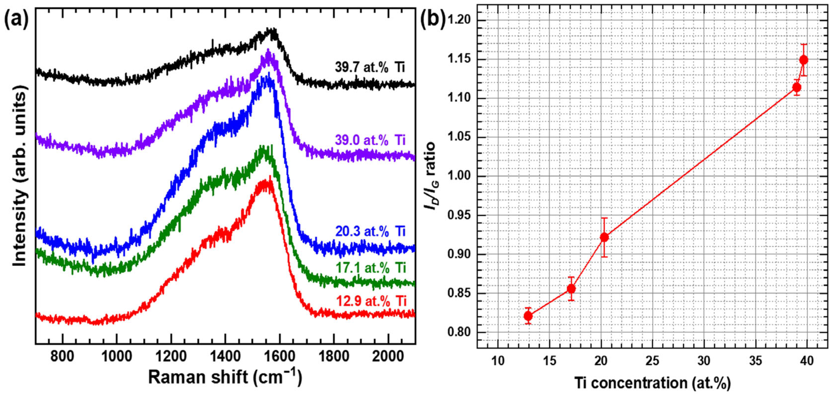
The Raman scattering spectra of the DLC:Ti films are presented in
Figure 1. Broad Raman scattering bands were observed in the range of 1000–1700 cm
−1, which can be divided into two characteristic peaks at 1200–1400 cm
−1 (D peak) and 1500–1600 cm
−1 (G peak). The former disorder-induced D peak (shoulder) is related to the breathing mode of sp
2 bonds, and the latter G peak was attributed to the stretching vibration mode of the sp
2 bond [
35].
Figure 1b illustrates the
ID/
IG values calculated from the Raman scattering spectra with respect to the Ti concentrations. Increasing the Ti concentration from 12.9 to 39.7 at.% produces an increase in the
ID/
IG ratio from 0.82 to 1.15. This indicates that the sp
2/sp
3 ratio increases with Ti addition. The Ti doping leads to graphitization of the films. An increase in the
ID/
IG ratio may suggest a higher sp
2/sp
3 ratio, but it does not necessarily correspond to an actual increase in the absolute sp
2 fraction.
The elemental compositions of the DLC:Ti films measured by EDS are shown in
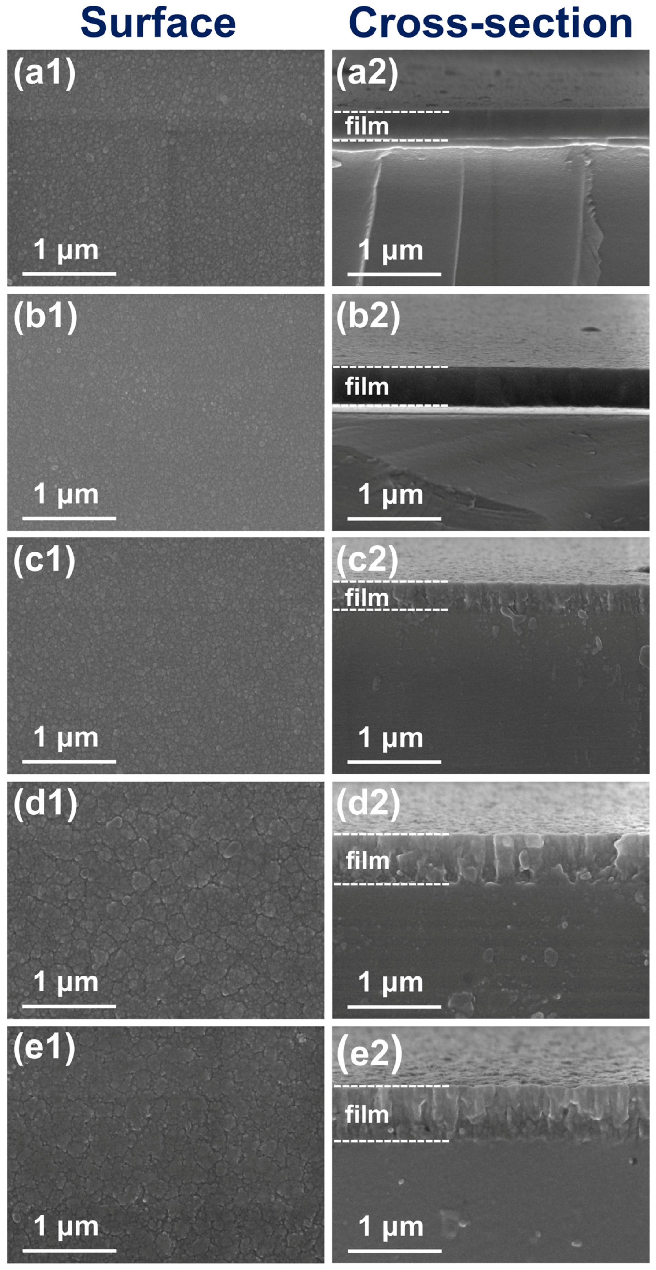
Table 1. The Ti concentration increases from 12.9 to 39.7 at.% as the Ti target power increases from 1300 to 1700 W. Surface and cross-sectional SEM images recorded from the DLC:Ti films are presented in
Figure 2. All thin films are dense and exhibit smooth surfaces without observable carbon particles. The surface of the films exhibits a granular microstructure. The average grain size increases with rising Ti content, while the compactness of the films gradually decreases. The film thickness increases from ~313 to 554 nm as Ti concentration increases from 12.9 to 39.7 at.%. The films exhibit a glassy-type cross-section when the Ti concentrations were below 17.1 at.%. However, a columnar structure was presented as the Ti concentration was increased up to 39.7 at.%.
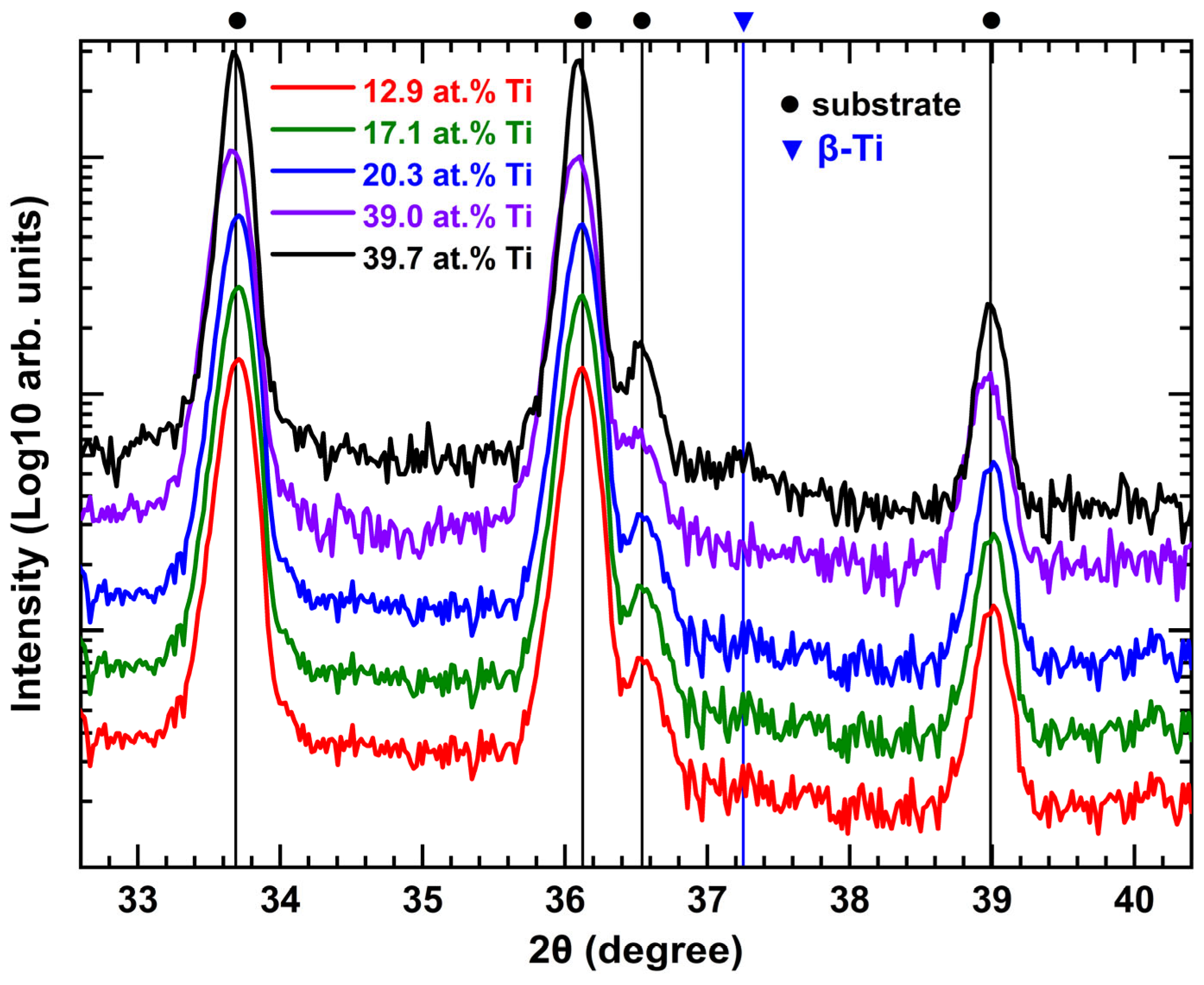
The X-ray diffraction (XRD) spectra of the DLC:Ti films are shown in
Figure 3. Those films do not show obvious peaks corresponding to the crystalline phase when the Ti content varies from 12.9 to 39.7 at.%. This implies that Ti exists either in an amorphous state or in nanoclusters within the film. The XRD method does not necessarily show peaks for crystalline metal particles with sizes below 2–3 nm [
25]. When the Ti content was increased up to 39.7 at.%, a weak diffraction peak corresponding to crystalline β-Ti appears.
The XPS analysis was applied to determine the chemical bonding states of the films.
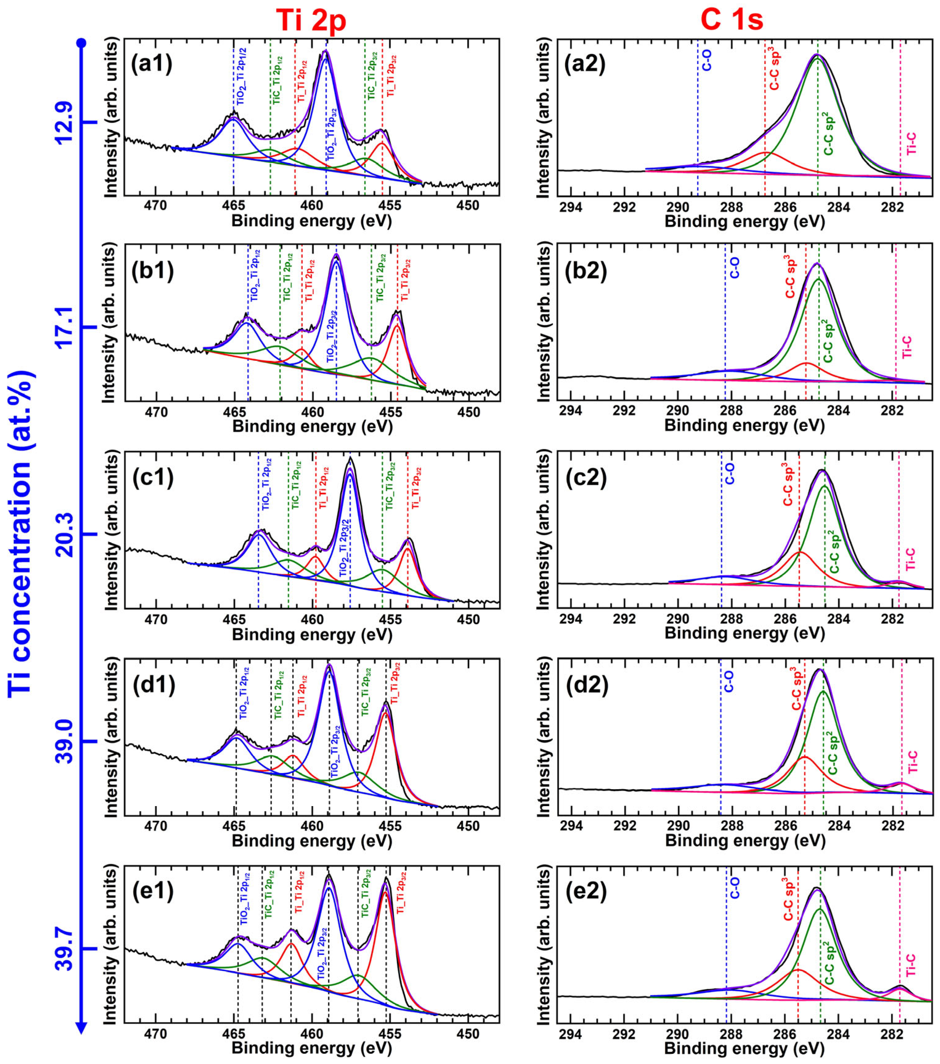
Figure 4 shows the fitted Ti 2p and the C 1s XPS spectra of the DLC:Ti films. The Ti 2p spectra in
Figure 4(a1,b1,c1,d1,e1) consisted of a spin–split 2p
3/2–2p
1/2 double state (ΔBE = 5.7 eV) attributed to Ti–Ti bonds [
36,
37,
38]. Since Ti was an oxyphilic element, TiO
2 was presented on the membrane surface under air exposure (corresponding to 458.5 and 464.2 eV).
Figure 4(a2,b2,c2,d2,e2) shows the C 1s spectra, including fitted peaks of C–C (C–sp
2) at 284.2 eV, C–C (C–sp
3) at 285.1 eV, C–O at 286.7 and 288.9 eV, and Ti–C at 282.5 eV [
39].
Figure 4(a1,b1,c1,d1,e1) shows the fitted Ti 2p spectra with respect to the Ti concentration. The intensities of the Ti 2p
1/2 and Ti 2p
3/2 peaks of the Ti–Ti and the Ti–C bonds increased with the increase in the Ti content in the DLC films.
Figure 4(a2,b2,c2,d2,e2) shows the fitted C 1s spectra with respect to the Ti content. The Ti–C peak intensity rises with Ti content, indicating that more Ti–C bonds form at higher Ti concentrations. The Raman and XPS analyses indicate that the addition of Ti promotes the graphitization of the DLC films [
39]. The absence of detectable TiC-related diffraction peaks in the X-ray pattern indicates that TiC was present in the film in a nanocluster state.
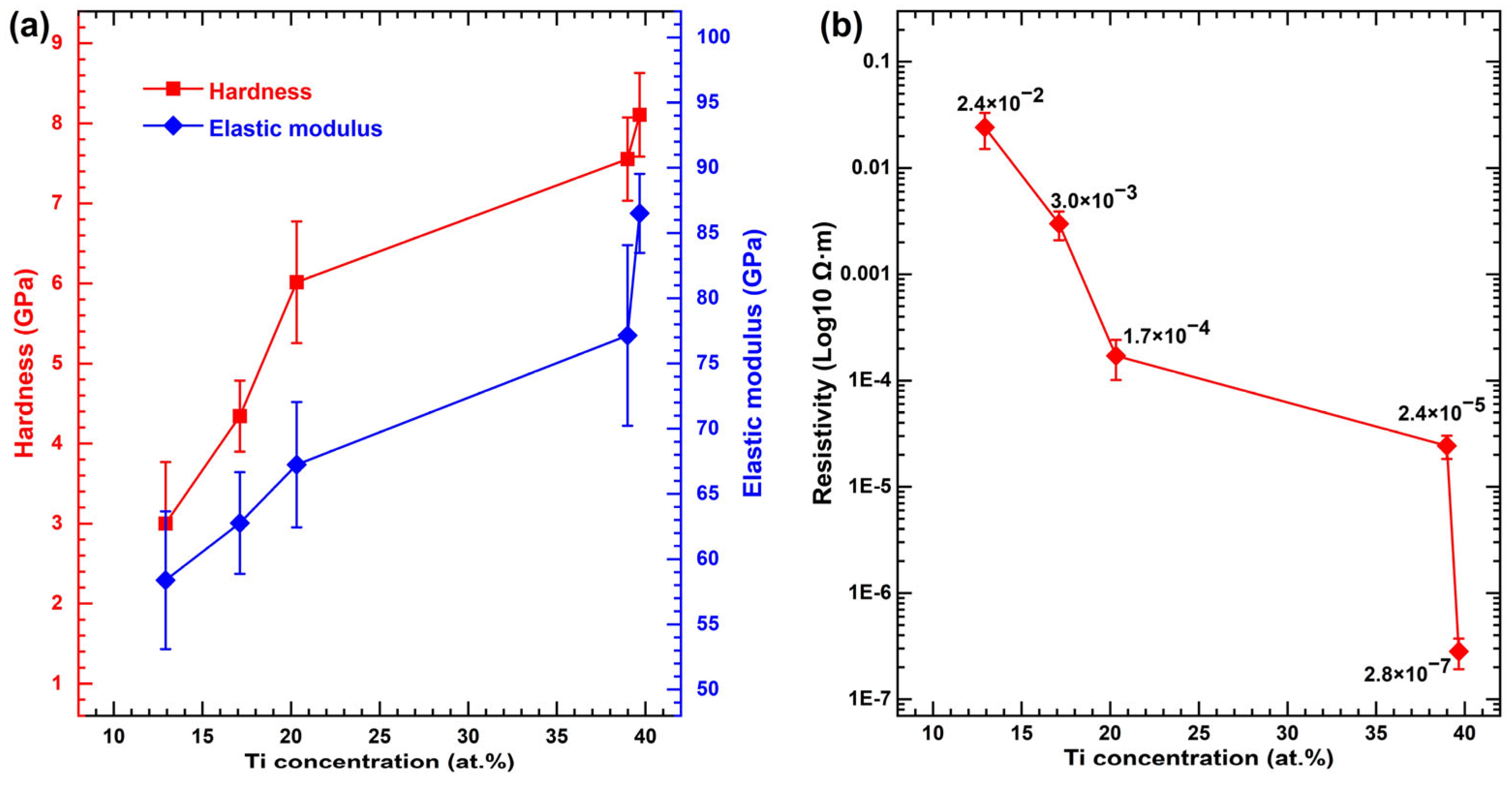
The indentation hardness and elastic modulus values of the DLC:Ti films with respect to the Ti content are shown in
Figure 5a. The film hardness increased from 3.0 ± 0.3 to 8.1 ± 0.4 GPa, and the elastic modulus increased from 58.4 ± 3.9 to 86.5 ± 3.7 GPa as the Ti concentration was increased from 12.9 to 39.7 at.%. The XPS analysis shows that increasing the Ti content promotes the formation of the Ti–C bonds in the films. This improves the film’s hardness and elastic modulus [
40]. The changes in electrical resistivity with respect to the Ti content are shown in
Figure 5b. Increasing the Ti content decreases the electrical resistivity of the films from 2.4 × 10
−2 Ω·m for 12.9 at.% Ti to 2.8 × 10
−7 Ω·m for 39.7 at.% Ti. Based on the above EDS, XPS, and Raman scattering results, the reasons for the decrease in electrical resistivity of the thin films are that the addition of the Ti component promotes the graphitization of the film, increasing the film conductivity.
The piezoresistive coefficient characterizes the sensitivity of thin films to mechanical deformation. Within a specific strain range, the linear correlation between the electrical resistance variation and applied strain is of critical importance, which is typically quantified by the linear correlation coefficient. For an ideal thin-film sensor, excellent linearity and a high piezoresistive coefficient
KP are two essential performance criteria.
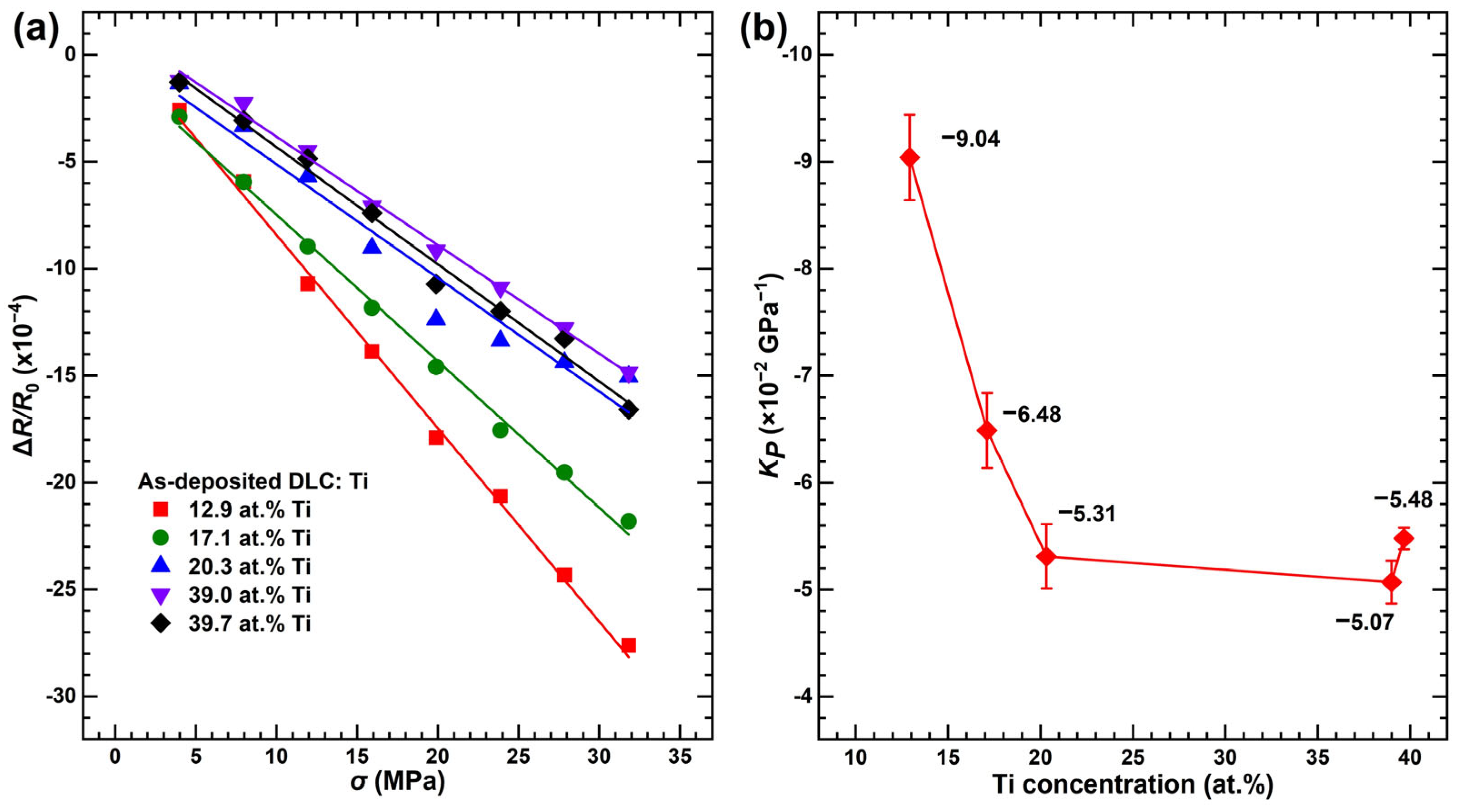
Figure 6a depicts the relationship between the electrical resistivity reduction in DLC:Ti films and applied load as a function of Ti concentration. The resistance reduction in DLC:Ti films exhibits a linear decrease with the increase in normal stress from 0 to 35 MPa, and a strong linear correlation is also maintained between the resistance reduction rate and normal stress. The maximum piezoresistive coefficient of DLC:Ti films was determined to be −9.0 × 10
−2 GPa
−1 at a Ti concentration of 12.9 at.%, and this coefficient decreases with the gradual increase in Ti content.
Figure 6b plots the piezoresistive coefficient versus the Ti concentration, showing a gradual decrease with increasing Ti. In addition, the
KP value of the DLC:Ti films is inversely proportional to the sp
2/sp
3 bond ratio [
14]. An increase in Ti content within the films leads to a reduction in sp
3 bond content, which in turn results in a decrease in the piezoresistive coefficient.
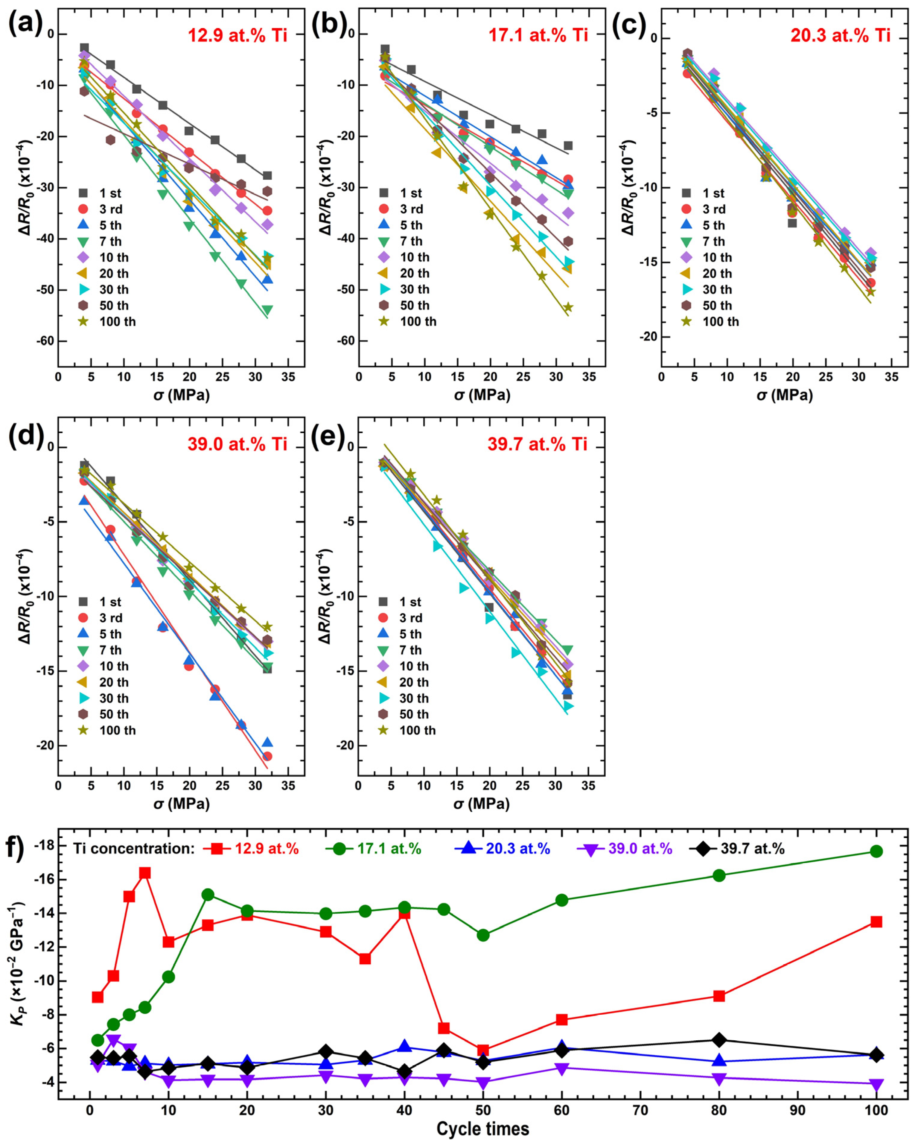
The repeatability of the piezoresistive coefficient is evaluated based on its consistency across multiple testing cycles under the same strain level. For an ideal sensor, excellent stability of this coefficient is an indispensable prerequisite. The variation in electrical resistivity of the DLC:Ti films with respect to the applied load after 1–100 piezoresistive test cycles is illustrated in
Figure 7a–e, while
Figure 7f presents the test results of the DLC:Ti films after 1–100 piezoresistive cycles. With the increase in normal stress, the electrical resistance of the DLC:Ti films decreases linearly. Moreover, an increase in loading cycles contributes to a higher stability of the piezoresistive coefficient for the DLC:Ti films. Specifically, films with a high Ti content exhibit a more stable piezoresistive coefficient compared to those with a low Ti content. Residual stresses in the films are relieved during cyclic compression. Meanwhile, graphitization of the carbon structure occurs, leading to variations in the piezoresistive coefficient after each individual piezoresistive test.
To investigate the mechanism underlying the evolution of the
KP values of the DLC:Ti films after 1–100 cyclic piezoresistive tests, Raman scattering spectroscopy was performed.
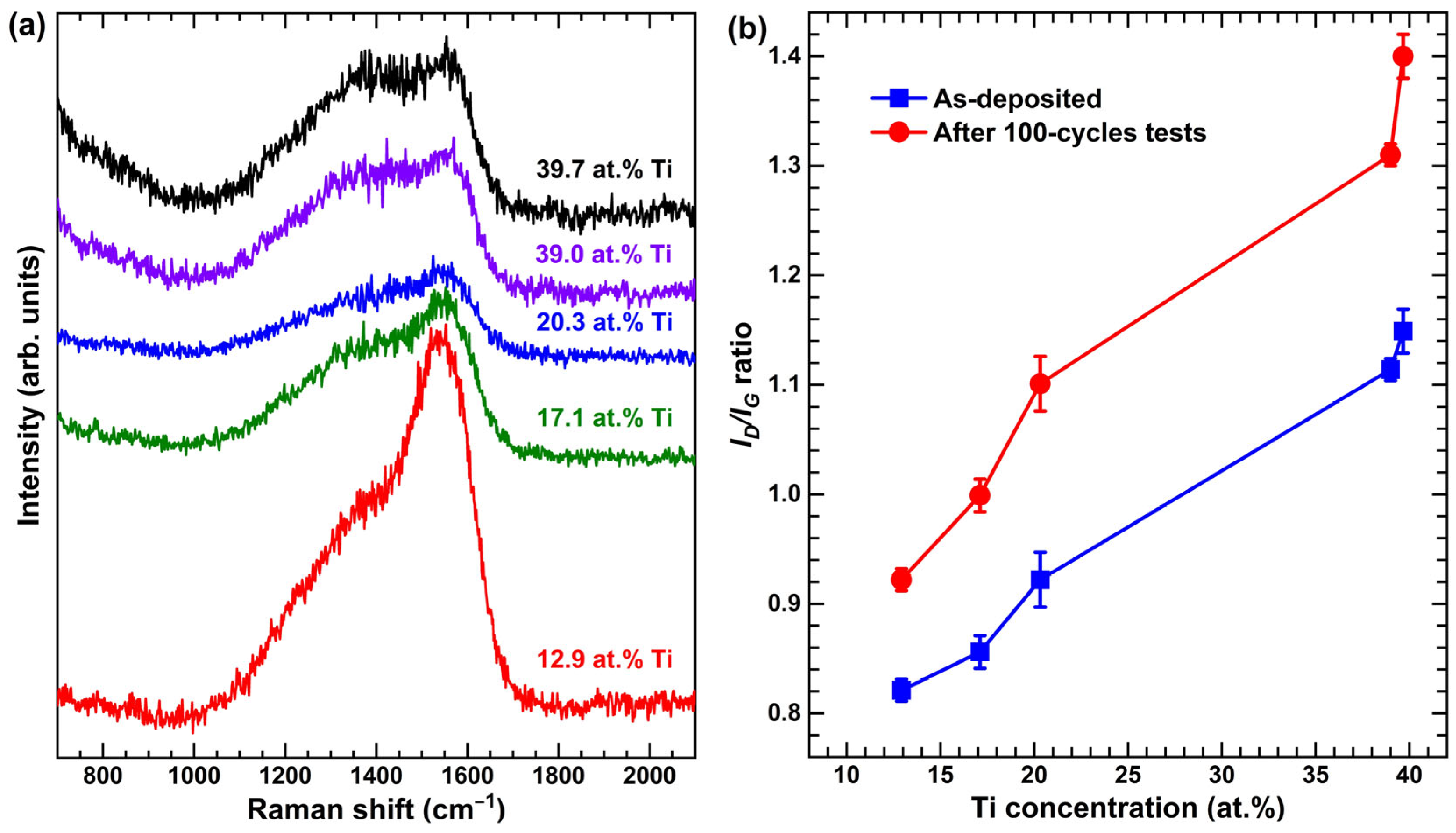
Figure 8a shows the Raman scattering spectra of the DLC:Ti films after 100 piezoresistive cycles under a maximum load of 31.8 MPa. The D and G peaks of carbon (C) are labeled at ~1350 cm
−1 and ~1580 cm
−1, respectively. As the Ti content increases, these peaks become weaker and broader.
Figure 8b presents the
ID/
IG values of the as-deposited DLC:Ti films and those after 100 piezoresistive cycles. The results indicate that the
ID/
IG values of the films increase after the tests, which suggests an increase in the sp
2/sp
3 ratio of the films and the occurrence of graphitization.
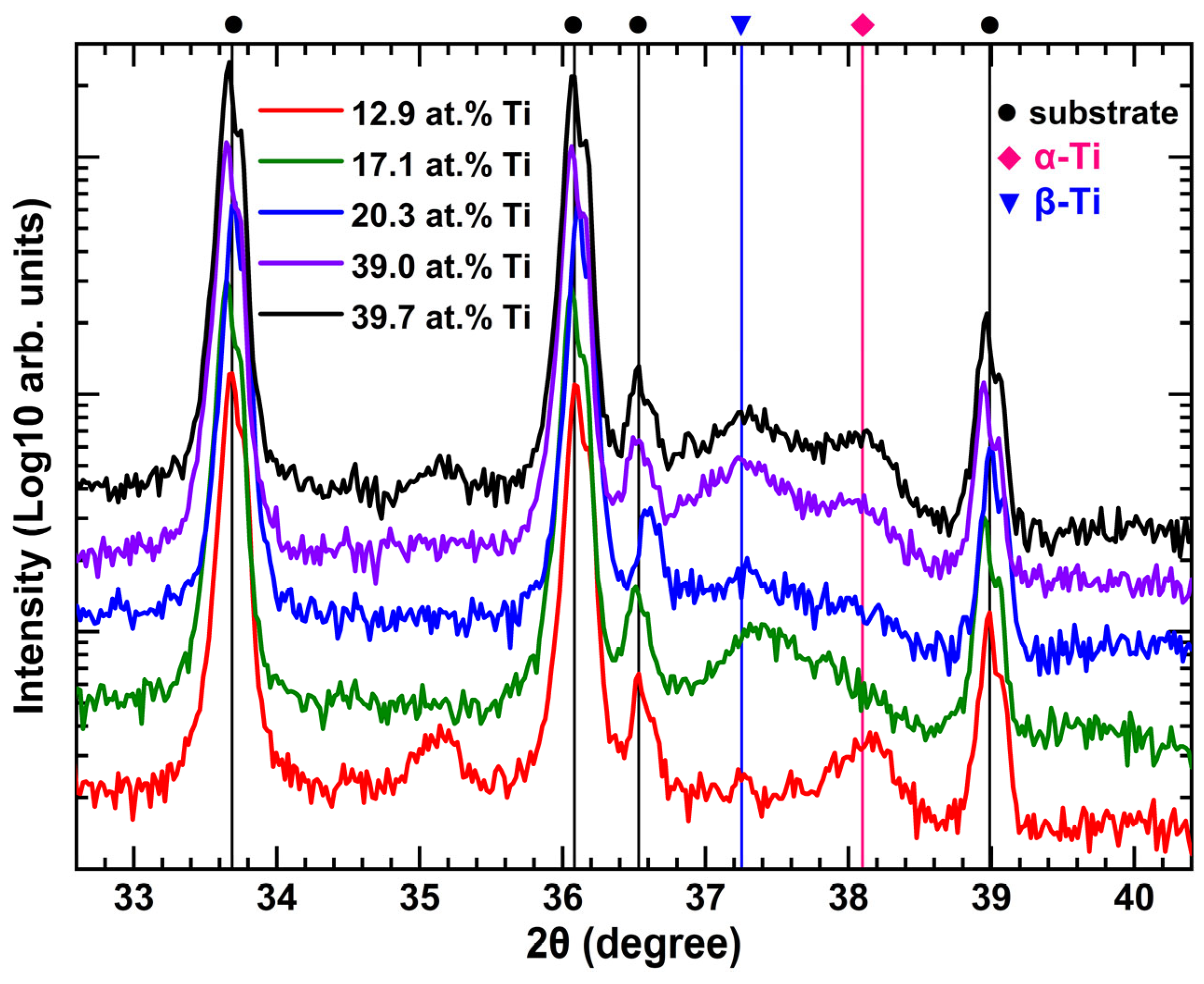
In addition, XRD tests were conducted on the DLC:Ti films after cyclic piezoresistive tests to explore the evolution of their phase structure.
Figure 9 displays the XRD patterns of the DLC:Ti films after 100 piezoresistive cycles. The compressed films exhibit α-Ti and β-Ti phases, and these phases become more prominent with increasing Ti content. In contrast, the as-deposited films with a Ti content of 12.9–39.0 at.% do not show crystalline α-Ti and β-Ti phases. This phenomenon demonstrates that the applied stress induces changes in the phase structure of the films, leading to the crystallization of Ti from a cluster or amorphous state to α-Ti and β-Ti phases.
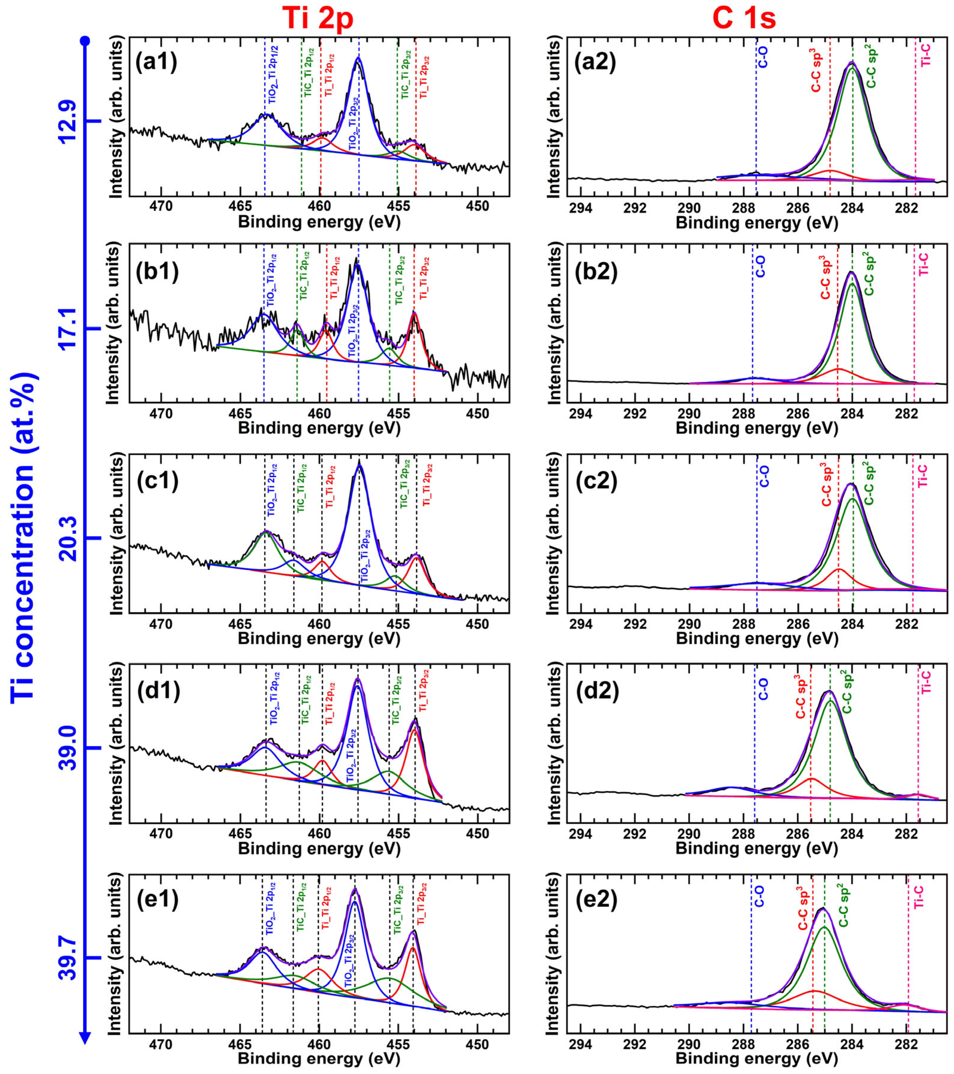
XPS was further employed to characterize the compressed DLC:Ti films, aiming to determine the changes in their chemical bonding structure. The XPS spectra of the DLC:Ti films after 100 piezoresistive cycles are shown in
Figure 10. The Ti 2p spectrum consists of a spin–split 2p
3/2–2p
1/2 doublet (ΔBE = 5.7 eV), which is attributed to Ti [
36,
37,
38]. TiO
2 is detected on the film surface due to exposure to air, corresponding to the binding energies of 458.5 eV and 464.2 eV. Additionally, the intensities of the Ti 2p
1/2 and Ti 2p
3/2 peaks corresponding to Ti–C bonds increase significantly with the increase in Ti content.
Figure 10(a2,b2,c2,d2,e2) show the C 1s XPS spectra, which can be deconvoluted into several peaks: C–C (C–sp
2) at 284.2 eV, C–C (C–sp
3) at 285.1 eV, C–O at 286.7 eV and 288.9 eV, and Ti–C at 282.5 eV [
39]. These figures also present the fitted C 1s peaks as a function of Ti content, revealing that the intensity of the Ti–C peak increases remarkably with the increase in Ti concentration in the DLC films. Compared with the results shown in
Figure 4, the intensity of the Ti–C bond decreases after the piezoresistive tests, indicating the occurrence of Ti–C bond breakage.
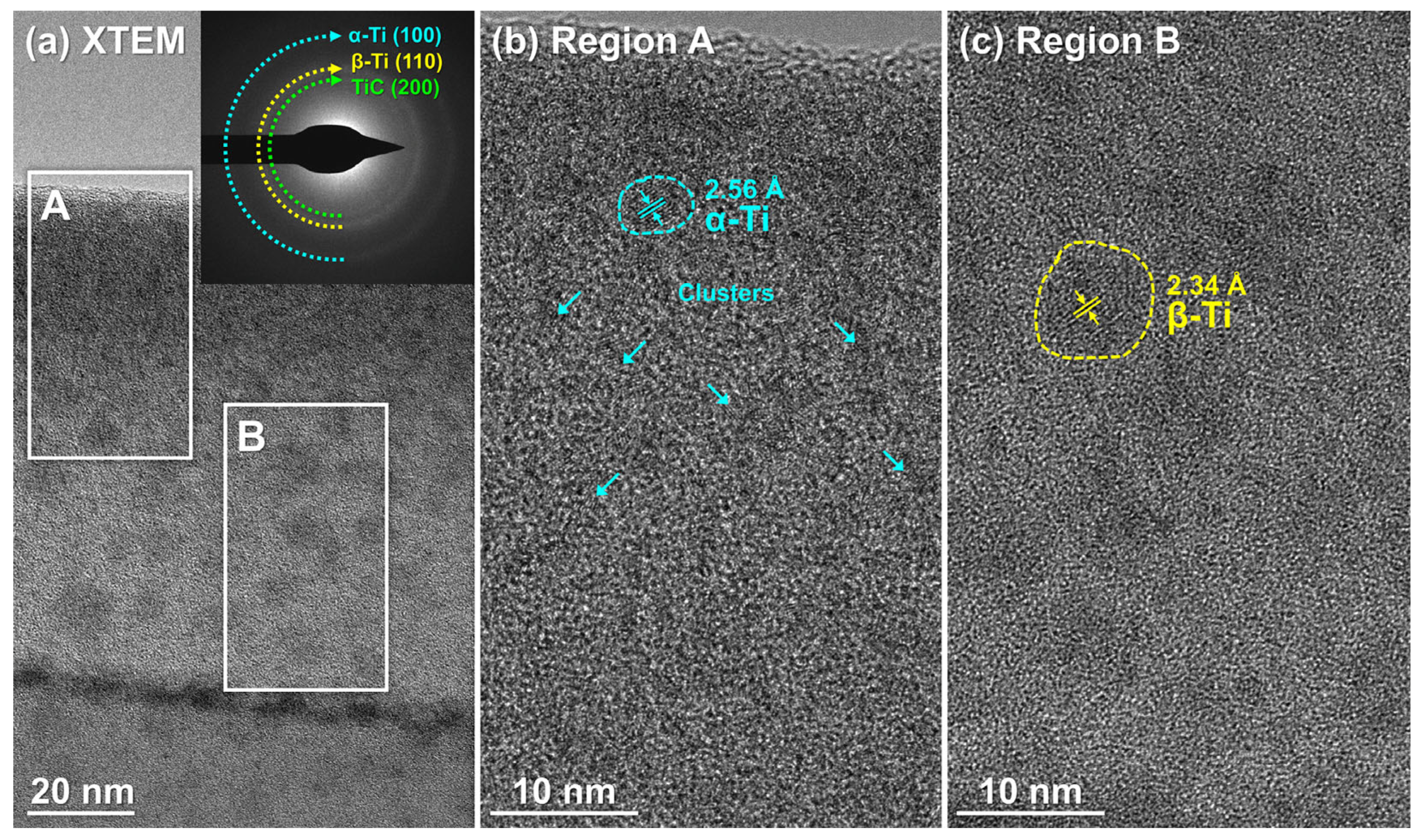
Figure 11 shows the transmission electron microscopy (TEM) images of the DLC:Ti film after 100 piezoresistive cycles. It can be observed that the clusters or grains in the top layer are more refined than those in the bottom layer, which may be attributed to the non-uniform stress distribution between the top and bottom layers of the film. A very weak diffraction ring corresponding to TiC is detected in the selected area electron diffraction (SAED) pattern. In addition, diffraction rings corresponding to α-Ti (100) and β-Ti (110) are also observed. High-resolution transmission electron microscopy (HRTEM) images reveal the presence of a large number of grains with dimensions on the nanometer scale. Both α-Ti (
Figure 11b) and β-Ti (
Figure 11c) grains can be noticed, agreeing well with the XRD results (
Figure 9). In contrast, the carbon matrix exhibits no discernible lattice fringes, indicating that carbon exists in an amorphous state. High-resolution transmission electron microscopy (HRTEM) images of the DLC:Ti film demonstrate that the film is dominated by amorphous carbon, along with extremely refined grains including α- and β-Ti.
4. Discussion
As shown in
Figure 1a, the D and G peaks in the Raman scattering spectra are characteristic of diamond-like carbon (DLC) films. With the increase in Ti concentration, these characteristic peaks exhibit a gradual decrease in intensity and broadening in profile. As illustrated in
Figure 1b, the incorporation of Ti facilitates the graphitization of the DLC films. Titanium is a strong carbide-forming element and preferentially forms Ti–C bonds during film growth. During the nucleation and subsequent growth of TiC nanoclusters, their crystal structure remains rigid and unable to accommodate excess carbon atoms, which are consequently expelled from the interfacial regions of TiC nanoclusters [
41]. The displaced carbon atoms with enhanced mobility tend to assemble into sp
2-hybridized graphitic domains with lower energy and higher structural stability, instead of reconfiguring into the highly stressed sp
3-hybridized carbon configuration. The introduced Ti atoms and the in situ formed TiC nanoparticles effectively disrupt the continuous sp
3 carbon network with high intrinsic stress in the DLC matrix. Owing to the distinct lattice constant of TiC relative to both graphite and diamond, these nanocrystalline inclusions act as stress relaxation centers in the amorphous carbon matrix. The reduction in the overall internal stress of the film releases the carbon atoms that were previously immobilized in the sp
3 state under high compressive stress, enabling their rehybridization and rearrangement into the more stable sp
2 configuration [
42]. Correspondingly, both the D peak (associated with disordered sp
2-hybridized carbon) and the G peak (characteristic of the total sp
2-hybridized carbon population) undergo broadening and intensity attenuation, which is attributed to the increased structural heterogeneity of the Ti-doped DLC films. Meanwhile, the systematic variation in spectral parameters such as the
ID/
IG ratio indicates a gradual increase in the number and size of sp
2 graphitic clusters, which directly confirms the enhanced graphitization degree of the DLC films with increasing Ti concentration.
As shown in
Figure 3, a crystalline β-Ti phase emerges in the film with a Ti concentration of 39.7 at.%. It is well established that the deposition process of DLC films is highly sensitive to the working temperature [
43]. With the increase in magnetron sputtering power during deposition, the Ti content in the film increases; simultaneously, the deposition temperature rises, which in turn leads to the attenuation of intensity and broadening of the D and G peaks in the Raman spectra.
The sputtering yield was closely associated with the energy of incident ions. Within a certain energy range (typically corresponding to the operating voltage in magnetron sputtering), an increase in sputtering power generally leads to a rise in both the voltage applied to the target and the target current [
44]. This further results in a simultaneous increase in the energy and density of Ar
+ ions bombarding the Ti target. Higher ion energy and flux significantly enhance the number of Ti atoms sputtered from the target surface per unit time, thereby increasing the sputtering rate of Ti atoms. Consequently, the flux of Ti atoms migrating toward the substrate increases, providing a more abundant Ti supply for film growth, which in turn leads to an increase in the Ti content in the as-prepared film.
When the Ti target power is set to 1700 W, the deposition temperature reaches its maximum value, and a small trace of crystalline β-Ti phase appears accordingly. Several factors contribute to the deposition temperature far exceeding the set point of the heater: the conversion of kinetic energy of sputtered Ti atoms and reflected Ar atoms into thermal energy upon their impact on the substrate surface, as well as the enhanced radiative heating from the denser plasma [
45]. This synergistic effect significantly elevates the actual temperature of the substrate and the growing film. The acquired thermal energy promotes atomic surface diffusion, allowing atoms to overcome energy barriers and migrate to positions corresponding to a more thermodynamically stable phase. Consequently, such a high deposition temperature facilitates the nucleation and growth of β-Ti crystals in the film.
Figure 4 illustrates the chemical bonding characteristics between Ti and C atoms. Moreover, the content of the Ti–Ti and the Ti–C bonds increases with the rise in titanium content. An elevated magnetron sputtering power leads to a higher deposition temperature, which in turn facilitates the formation of Ti–C bonds. As the titanium content increases, more Ti atoms are available in the deposition system to bond with C atoms; despite the decrease in the relative proportion of C atoms, the absolute number of Ti atoms rises remarkably, resulting in an overall increase in the quantity of Ti–C bonds within the system [
46]. When the titanium content further increases and exceeds the stoichiometric ratio of Ti to C (i.e., Ti:C > 1:1), a titanium excess state is formed. The excessive Ti atoms cannot find sufficient C atoms for Ti–C bond formation and thus tend to bond with other surplus Ti atoms instead. Accordingly, the number of metallic Ti–Ti bonds increases significantly, which enhances the electrical conductivity of the film and renders its metallic properties more prominent [
47].
Higher deposition temperatures endow the Ti and C atoms adsorbed on the substrate surface with greater kinetic energy, enabling their freer migration. This increases the probability of atomic collision and assembly of Ti and C atoms at the thermodynamically most stable low-energy lattice sites, thereby promoting the formation of stable Ti–C chemical bonds. The formation of new Ti–C bonds requires Ti and C atoms to overcome a certain energy barrier by breaking their original chemical bonds, and the elevated temperature provides the necessary activation energy for this reaction, making the formation of Ti–C bonds kinetically favorable. Furthermore, high temperatures facilitate the local structural relaxation of atoms after bonding, which optimizes the bond lengths and bond angles of Ti–C and thus contributes to the formation of more stable and robust Ti–C bonds.
Notably, no crystalline TiC phase was detected in the XRD patterns of the films, indicating that TiC exists in an amorphous or nanocluster state in the prepared films. During the non-equilibrium magnetron sputtering deposition process, atoms are impinged onto the substrate at an extremely high rate, leaving insufficient time for the atoms to arrange into an ordered crystalline structure upon deposition [
48]. Even if the sputtering power-induced heating elevates the deposition temperature, the temperature remains below the crystallization temperature of TiC when the heating effect is insufficient, which restricts the atomic mobility. As a result, the atoms are kept in a disordered, random configuration, forming an amorphous structure. Short-range atomic order is still present in this amorphous structure: each Ti atom is coordinated with adjacent C atoms and vice versa, forming individual Ti–C bonds. However, this short-range order is only maintained over a few atomic distances and lacks the long-range periodic arrangement that extends over tens of atomic scales or more. Since XRD is insensitive to such short-range structural order, only broad hump-like diffraction peaks or no distinct crystalline diffraction peaks are observed in the XRD patterns. Even if tiny TiC crystallites form in local regions of the film, no sharp XRD peaks can be generated when the crystallite size is extremely small (typically less than several nanometers). Consequently, the TiC formed in the films predominantly exists either as an amorphous network with only short-range atomic order or as ultra-fine nanocrystals/nanoclusters, and neither of these structural forms can produce well-resolved crystalline diffraction peaks in XRD measurements.
Figure 11 further verifies that TiC exists in the thin film as nanoclusters.
Figure 2 reveals that the average particle size increases with rising Ti concentration, with the maximum observed for the film with a Ti concentration of 39.7 at.%. When the Ti concentration is below 17.1 at.%, the film cross-section exhibits a glassy microstructure. At low Ti concentrations, a carbon-rich amorphous network with strong covalent bonding constitutes the dominant phase, with a small fraction of Ti atoms incorporated into and bonded within this network [
47]. Instead of inducing crystallization, these dilute Ti atoms increase the structural chemical disorder, thereby stabilizing the amorphous phase and inhibiting the nucleation and growth of crystalline domains. For Ti concentrations ranging from 20.3 to 39.7 at.%, the film cross-section displays a columnar structure. At moderate Ti concentrations, the increased Ti content provides the requisite compositional basis for TiC nucleation. Furthermore, metallic Ti–Ti bonds enhance atomic mobility [
46]. Under conditions of limited surface diffusion, the system undergoes a competitive growth mechanism, leading to the precipitation and development of a typical columnar polycrystalline structure from the amorphous matrix.
The evolution of the piezoresistive properties of the DLC:Ti films is presented in
Figure 6. With the applied normal stress increasing from 0 to 35 MPa, the film resistance exhibits a linear decrease. Previous studies have reported that DLC:Ti films yield the maximum piezoresistive coefficient
KP at low Ti concentrations, typically on the order of 10
−2 GPa
−1 [
49,
50], which is consistent with the experimental results obtained in this work. This phenomenon is primarily attributed to the stress-induced enhancement of the conductive network and the modulation of electron tunneling effects. Applied stress reduces the average interspacing between conductive clusters; for electron transport paths originally governed by tunneling, even a slight reduction in the barrier width can lead to an exponential increase in the electron tunneling probability [
49]. The observed near-linear resistance decrease mainly arises from the compressive stress narrowing the gaps between conductive nanoclusters, which significantly enhances the inter-cluster quantum tunneling conductance.
The piezoresistive coefficient of the films decreases with increasing Ti content, which is associated with the reduction in sp
3 hybridization content induced by elevated metallic Ti incorporation—this in turn leads to an increase in the intrinsic electrical conductivity of the films. At low Ti contents, quantum tunneling dominates the charge transport mechanism [
51]. Given that tunneling is highly sensitive to the inter-cluster distance, the application of external stress can induce a large relative change in resistance [
52], resulting in a pronounced piezoresistive effect and a correspondingly high gauge factor. In contrast, at high Ti contents, the sp
3-to-sp
2 structural transition (graphitization) occurs in the carbon matrix; the resulting sp
2 carbon clusters are intrinsically excellent electrical conductors, which significantly reduce the resistivity of the carbon matrix itself. Furthermore, the reduction in sp
3 content softens the originally rigid DLC matrix, leading to a decrease in its Young’s modulus. Under the same applied stress, this softened matrix undergoes a larger strain [
43]; however, this increased strain is less effective in transmitting and modulating the tunneling distances within the conductive network compared to the rigid matrix, resulting in an attenuated piezoresistive response. Meanwhile, at high titanium contents, a percolating Ti/TiC network is formed, and the system transitions into a metal-like conduction state. In this regime, the piezoresistive response primarily originates from the strain-modulated tunneling gap variations within the Ti/TiC percolation network under external mechanical loading. At this stage, the further reduction in sp
3 content is no longer the dominant parameter governing the gauge factor.
The overall decrease in the gauge factor with increasing Ti content thus originates from the film’s electronic state transition—from a semiconducting state governed by the highly stress-sensitive tunneling mechanism to a conductive state dominated by the less stress-sensitive metallic conduction mechanism [
50]. The substantial reduction in the baseline resistance, combined with this shift in the dominant charge transport mechanism, collectively impairs the relative effectiveness of external stress in modulating the film resistance.
Figure 5 presents the hardness, elastic modulus and electrical resistivity of the DLC:Ti films. XPS analysis reveals that an increase in Ti content leads to the formation of more Ti–C bonds in the films. XRD and TEM characterizations confirm that TiC exists in a nanocrystalline state within the films. A significant increase in hardness from 3.0 to 8.1 GPa is observed with increasing Ti content. This trend stands in apparent contradiction to the graphitization (i.e., an increased sp
2/sp
3 ratio) inferred from Raman spectroscopy, as graphitization is conventionally associated with mechanical softening. Rather than contradicting the expected trend, this hardness enhancement actually reveals the dominance of competing mechanisms within the Ti-doped DLC system. This enhancement in mechanical properties is primarily attributed to the intrinsically excellent mechanical properties of Ti–C bonds and their reinforcing and hardening effects on the amorphous carbon matrix. Ti–C bonds tend to form ultra-hard TiC nanocrystals or amorphous TiC clusters, and these nanoscale hard phases are uniformly dispersed in the relatively soft amorphous carbon matrix [
49]. The increase in Ti–C bonds effectively produces the formation of plenty of tiny rigid nanoclusters and strong cross-linking sites into the films; these structural features enhance the deformation resistance of the films both via their inherent high bond strength and stiffness and by impeding shear deformation and reinforcing the overall carbon network, thus significantly improving the macroscopic hardness and elastic modulus of the films [
53].
Reported studies indicate that DLC:Ti films exhibit a hardness peak (typically ~12 GPa) at an optimal Ti content, with a subsequent decrease in hardness upon further Ti incorporation [
46,
54]. This hardness decline is ascribed to the formation of an excessively soft metallic Ti phase at high Ti contents, which preferentially deforms under applied load and thus softens the composite matrix. In contrast, in this work, Ti primarily forms hard amorphous Ti–C phases or ultra-fine TiC nanocrystals rather than large, soft metallic Ti clusters. This distinct microstructure evolution accounts for the absence of a hardness peak in the prepared DLC:Ti films. In the present work, titanium predominantly forms a hard amorphous Ti–C phase or ultra-fine TiC clusters rather than crystalline TiC. This leads to a lower hardness compared with reported films containing crystalline TiC. Furthermore, an extremely low electrical resistivity of 2.82 × 10
−7 Ω·m is achieved for the film with a Ti concentration of 39.7 at.%, which is very close to the resistivity of bulk titanium and lower than most reported values for films with a similar Ti content [
26].
The underlying mechanisms governing the variation in piezoresistive properties of the DLC:Ti films were systematically analyzed. XRD, Raman scattering, and XPS characterizations were conducted on the films following 1–100 cycles of piezoresistive testing. The observed trend in piezoresistive stability is consistent with the previous literature reports [
51,
55], where films with higher metallic content typically exhibit improved piezoresistive repeatability. In the present work, however, a notably smaller variation in the piezoresistive coefficient was observed, indicative of superior performance stability of the prepared films. Raman spectra obtained after 100 piezoresistive cycles reveal a structural evolution of the carbon matrix in the DLC:Ti films, with an increase in the
ID/
IG ratio implying the occurrence of stress-induced graphitization. This graphitization process is driven by mechanical stress and is characterized as a stress-assisted, thermally activated transformation. The amorphous DLC network contains numerous sp
3 carbon atoms with bond-angle distortions and distorted sp
2 carbon rings, rendering the matrix in a metastable thermodynamic state. Cyclic compressive stress imposes periodic shear and hydrostatic stress components on the carbon network, and this repeated mechanical perturbation promotes the rupture of weak, highly strained C–C covalent bonds [
26]. Once a bond is fractured, carbon atoms are guided by the stress field to reorganize into more stable, planar sp
2 configurations with lower in-plane strain energy—a process defined as stress-induced structural transformation. Furthermore, under the synergistic effect of cyclic stress and localized frictional heating, titanium atoms or TiC nanocrystals at the amorphous carbon/TiC interface can significantly reduce the activation energy required for the sp
3-to-sp
2 transition [
55]. Titanium thus facilitates the rearrangement of carbon atoms and accelerates the growth of graphitic crystallites, leading to a more pronounced increase in the
ID/
IG ratio.
XPS characterizations post 100 piezoresistive cycles show a decrease in the intensity of the Ti–C bond characteristic peak for the DLC:Ti films, confirming the fracture of Ti–C bonds during cyclic loading. XRD patterns of the compressed DLC:Ti films reveal a mixed phase of α- and β-Ti, which is attributed to two key stress-induced effects: the breakage of Ti–C bonds and the relaxation of internal stress in the films, as well as the β- to α-Ti phase transformation under external loading. When external compressive stress is applied to the film, the resulting stress is non-uniformly distributed within the material matrix. Although Ti–C bonds possess intrinsically high bond strength, they undergo fracture when the local stress exceeds their critical bonding strength. Under cyclic compressive stress, stress concentration sites within the film generate local stress levels far exceeding the average applied stress, and these localized stress fields ultimately induce the rupture of even the relatively strong Ti–C bonds [
54]. Additionally, the as-deposited films may contain a metastable β-Ti phase formed during the non-equilibrium magnetron sputtering process; cyclic stress provides both the thermodynamic driving force and kinetic pathway for the transformation of this metastable phase [
56]. During loading–unloading cycles, a fraction of the β-Ti phase transforms into the thermodynamically stable α-Ti phase, while the remaining β-Ti persists due to kinetic barriers or local compositional inhomogeneities, resulting in the coexistence of α- and β-Ti phases.
The fracture of the Ti–C bonds creates localized pathways for stress relaxation in the surrounding compressed carbon network, enabling slight atomic rearrangements into more relaxed, lower-energy configurations and thus releasing a portion of the stored elastic strain energy. The cumulative effect of numerous microscopic bond fractures and local atomic rearrangements manifests macroscopically as a significant reduction in the overall internal stress of the DLC:Ti films.