Article

Reliability Study and Lifetime Prediction of 270 nm AlGaN-Based Deep Ultraviolet Light-Emitting Diodes

1
State Key Laboratory of Widegap Semiconductor Optoelectronic Materials and Technologies, North University of China, Taiyuan 030051, China
2
Institute of Semiconductors, Chinese Academy of Sciences, Beijing 100083, China
3
University of Chinese Academy of Sciences, Beijing 100190, China
4
Shanxi Semiconductor Deep Ultraviolet Technology Innovation Center, Advanced Ultraviolet Optoelectronics Company Ltd., Changzhi 046000, China
*
Authors to whom correspondence should be addressed.
Coatings 2026, 16(5), 597; https://doi.org/10.3390/coatings16050597
Submission received: 21 April 2026 / Revised: 12 May 2026 / Accepted: 12 May 2026 / Published: 14 May 2026

Abstract

AlGaN-based deep ultraviolet light-emitting diodes (DUV LEDs) have been widely deployed in water treatment, sterilization, and optical communication owing to their intrinsic merits of mercury-free operation, compact footprint, and fast turn-on capability. However, poor reliability and short operating lifetime, mainly caused by electrical degradation and poor heat dissipation, have severely limited their commercial applications. In this work, the degradation mechanism of 270 nm DUV LEDs was systematically studied via multi-condition accelerated aging tests. Results confirm that electrical stress is the dominant factor inducing device degradation, while thermal stress plays a secondary role. Electrical stress generates internal defects, increases leakage current and thermal resistance, enhances non-radiative recombination, and causes a sharp drop in light output power. Based on test data, the L70 lifetimes predicted by the inverse power law and the Arrhenius models are 5832 h and 5724 h, with relative errors of 8.59% and 10.28% compared with the measured 6380 h. This work provides reliable experimental support for the performance evaluation and lifetime prediction of DUV LEDs.

1. Introduction

AlGaN-based deep ultraviolet light-emitting diodes (DUV LEDs) exhibit intrinsic merits of mercury-free operation, compact footprint, and rapid turn-on capability [1,2]. They have been widely deployed in water and air purification, sterilization, biochemical detection, and secure optical communication, and are gradually replacing traditional mercury lamp sources in these fields [3,4]. The strict restrictions on mercury-containing products imposed by the Minamata Convention have directly driven the growing market demand for DUV LEDs as an eco-friendly alternative [5]. Meanwhile, the COVID-19 pandemic has significantly raised public awareness of and demand for high-efficiency deep ultraviolet sterilization technology [6], which further expands the application scenarios of DUV LEDs in public health, medical disinfection, and water treatment. These combined factors provide a strong impetus for the rapid industrial development of high-performance DUV LEDs.
In recent years, the electro-optical performance of AlGaN-based DUV LEDs has been significantly improved through innovations in epitaxial growth, device structure design, and packaging technology [7,8,9]. However, compared with mature visible-light InGaN/GaN-based LEDs, critical drawbacks, including short operating lifetime and poor long-term reliability, remain the primary bottlenecks limiting their large-scale commercial application [10,11]. To break through this bottleneck, it is essential to systematically elucidate the degradation mechanism of devices under operating stress and establish an accurate lifetime prediction method, which has attracted extensive attention from the academic and industrial communities. In terms of degradation mechanism research, Piva et al. conducted reliability studies on 285 nm and 300 nm DUV LEDs, and found that device degradation is mainly associated with defect-induced enhancement of Shockley–Read–Hall (SRH) non-radiative recombination [12,13]. In terms of lifetime prediction, Park et al. fabricated a 280 nm DUV LED with a Ni-doped AlN transparent ohmic electrode, which delivered an optical output power of 11.6 mW at 100 mA, and predicted an L50 (LOP decays to 50% of the initial value) lifetime of 2107 h via the Arrhenius model [14]. Chen et al. designed a triangular island-type p-type electrode structure to suppress current crowding and achieved a predicted L70 lifetime of 3460 h based on the ABC model [15]. Ruschel et al. investigated the current-induced degradation behavior of 310 nm UV LEDs at a fixed temperature, derived that the device lifetime is inversely proportional to the cube of the current density, and established a corresponding lifetime prediction model [16]. Despite the above progress, there are still three critical research gaps to be filled: First, most existing studies focus on DUV LEDs with emission wavelengths above 280 nm, while systematic investigations on the degradation mechanism and lifetime prediction of 270 nm short-wavelength DUV LEDs (with higher Al composition and more prominent reliability issues) are still insufficient, despite their higher sterilization efficiency and wider application prospects in the disinfection field. Second, most previous studies couple electrical and thermal stress for degradation analysis, failing to clearly distinguish the independent contribution and primary–secondary relationship of the two stresses, which makes it impossible to accurately locate the core inducement of device degradation. Third, most existing lifetime prediction studies only complete model fitting, lacking systematic verification and error analysis of the predicted results through long-term measured lifetime, which makes it difficult to guarantee the prediction accuracy and guide practical engineering applications.
In this work, we take 270 nm AlGaN-based DUV LEDs as the research platform, which deliver a light output power (LOP) of 22 mW at 100 mA and a measured maximum L70 lifetime of 6380 h under rated operating conditions. We carry out systematic reliability analysis and lifetime prediction of the devices through single electrical stress and thermo-electrical combined stress accelerated aging tests. We analyze the evolution of the optical, electrical, and thermal characteristics of the devices after 1000 h of accelerated aging, and clarify that electrical stress is the dominant factor triggering device degradation, while thermal stress only plays a secondary auxiliary role. Specifically, electrical stress induces activation and generation of intrinsic defects in the chip, which increases leakage current and thermal resistance, aggravates non-radiative recombination, and ultimately leads to a sharp drop in LOP. Furthermore, we predict the device lifetime via the inverse power law model and the Arrhenius model, and verify the prediction accuracy of the two models by comparing the predicted results with the measured lifetime. This work provides solid experimental evidence and theoretical guidance for the reliability evaluation and lifetime prediction of AlGaN-based DUV LEDs, and is of great significance for promoting their large-scale practical engineering applications.

2. Experimental Details

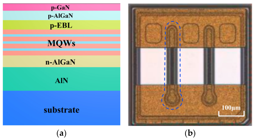
The DUV LED wafer was grown using a metal–organic chemical vapor deposition (MOCVD) system. As shown in Figure 1a, the growth process started with a 2.4 µm-thick AlN buffer layer on a sapphire substrate, followed by a 1 µm-thick n-Al0.6Ga0.4N layer. Subsequently, three periods of 2 nm-thick Al0.45Ga0.55N/12 nm-thick Al0.56Ga0.44N multiple quantum wells (MQWs) were deposited. This was followed by a 40 nm-thick Mg-doped p-Al0.8Ga0.2N electron blocking layer (p-EBL), a 20 nm-thick p-AlGaN layer with an aluminum composition graded from 0.75 to 0.35, and a 2 nm-thick p-GaN contact layer. After epitaxial growth, the mesa structure was formed by dry etching to expose the n-AlGaN layer. Cr/Al/Ti/Au and Ni/Rh/Ni multi-layers were deposited as n-electrode and p-electrode, respectively. Then, 800/20/100 nm-thick Ti/Pt/Au metal pads were deposited on both the n- and p-electrodes. Finally, after thinning the sapphire substrate to 400 µm, the wafer was diced into 0.5 mm × 0.5 mm chips via laser stealth dicing. Figure 1b shows a top-view optical micrograph of the DUV LED chip from the electrode side. The metallic-colored regions at the upper and lower parts of the image correspond to the p-contact and n-contact, respectively. The white areas underneath are the p-GaN mesa, and the two deep trenches (marked by blue dashed lines) are etched down to the n-AlGaN layer.
A batch of AlGaN-based DUV LED chips with uniform performance parameters was selected from the same wafer, which exhibited a peak emission wavelength of 270 nm and an average LOP of 22 mW at an operating current of 100 mA. The chips were flip-chip bonded onto AlN ceramic substrates using AuSn alloy solder, followed by die bonding in a eutectic furnace at 330 °C to enhance the interfacial bonding strength. Finally, quartz glass was bonded to the dam structure of the ceramic holder with an organic adhesive to finish the device packaging. During the aging test, to simulate the actual operating conditions, the AlGaN-based DUV LEDs that had completed the initial performance characterization were soldered onto aluminum-based PCBs to ensure stable electrical connections and good heat dissipation. Specifically, every 10 LEDs were mounted on the front surface of the PCB with flux-containing solder paste and soldered by a staged temperature-controlled reflow soldering process. The PCB was then fastened to a heat sink with screws, which effectively avoids poor electrical contact and local overheating, thus ensuring the accuracy and reliability of the aging test results. The test samples were divided into five groups, each containing 10 LEDs.
Each group was subjected to different stress conditions for aging tests, with the detailed parameters listed in Table 1. The ambient temperature of the samples was precisely controlled by a constant-temperature aging test chamber. Based on the type of stress applied, the samples were divided into two groups for comparative analysis: Group 1 was subjected to the same temperature but different currents and was defined as the electrical stress test group; Group 2 was subjected to the same current but different temperatures and was defined as the combined thermal–electrical stress test group. The aging tests for each group were terminated when the average LOP dropped below 70% of its initial value. Prior to the accelerated aging tests, variable-current measurements were conducted on the samples using a photoelectric analysis system (ATA-500, Everfine, Hangzhou, China). During characterization, the LOP was measured with a UV LED module radiation test system, the current–voltage (I–V) characteristic curves were acquired using a Keithley 2460 source meter (Keithley Instruments, Inc., Cleveland, OH, USA), and the thermal resistance was tested with a transient thermal tester (T3Ster, Siemens Digital Industries, Budapest, Hungary).
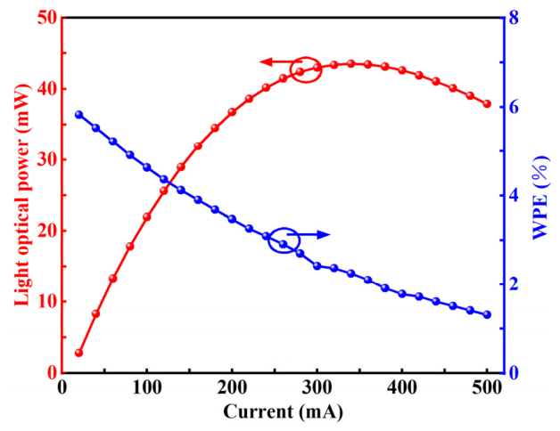
Figure 2 presents the LOP and wall-plug efficiency (WPE) of the LEDs before aging at various test currents. The test current ranged from 20 mA to 500 mA with a step of 20 mA, and the test temperature was maintained at 25 °C. The LOP of the DUV LEDs first increases and then decreases with increasing current, reaching a peak of 43.5 mW at 340 mA; the LOP is 21.94 mW at the typical operating current of 100 mA. The WPE decreases monotonically with rising current; it is 4.63% at 100 mA and 2.25% at 340 mA with peak LOP. Although the device reaches its peak LOP at 340 mA, this current is not an ideal operating current. The device exhibits a low WPE at 340 mA, and high-current operation generates substantial Joule heat. On the one hand, high temperature causes a significant thermal quenching effect [17], and this peak LOP is only an instantaneous value. Continuous operation increases the junction temperature and results in a sharp drop in LOP. On the other hand, high temperature accelerates defect multiplication in the active region, as well as Mg atom diffusion and ohmic contact degradation [12,18]. This leads to irreversible degradation of the optoelectronic performance. Considering practical applications and factors such as heat dissipation, 100 mA is selected as the optimal operating current of the device. Based on the above analysis, 100 mA, 200 mA and 300 mA are used as the test currents for the aging tests.

3. Results and Discussion

3.1. Optical Properties

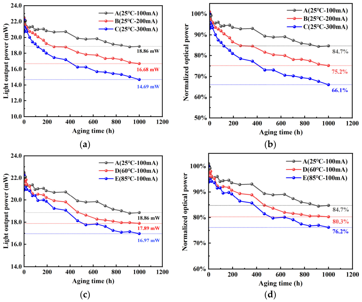
Under accelerated stress conditions, the samples exhibited a rapid decline in optical power. All the samples were measured at a current of 100 mA. Figure 3 shows the trends of LOP and normalized LOP for samples when aged for 1000 h under different stress conditions. As shown in Figure 3a,b, after the 1000 h aging test, the average LOP of samples A, B, and C decreased to 18.86 mW, 16.68 mW, and 14.69 mW, with corresponding declines of 15.3%, 24.5%, and 33.9%, respectively. In the early aging stage (the first 400 h), the LOP degrades rapidly with stress duration, and higher electrical stress causes faster degradation. This phenomenon stems from the activation of intrinsic defects (lattice defects, dislocations, etc.) in the material by electrical stress; such defects are unavoidable during the fabrication of DUV LEDs. In the early stages of degradation, Shockley–Read–Hall (SRH) recombination [19], facilitated by these defects, dominates. As recombination centers, they reduce the radiative recombination efficiency of carriers, thereby causing a rapid decline in LOP. However, during this period, the LOP sometimes remains constant or even increases slightly. This is because electrical stress activates the passivated Mg acceptors [20], leading to an improvement in radiative recombination efficiency that offsets or even exceeds the optical degradation. Meanwhile, environmental factors during testing could also have a slight impact. In the later stage of stress, the LOP degradation rate slows down noticeably, indicating that the defect concentration near the MQWs gradually saturates.
The trends of LOP and normalized LOP for samples when aged for 1000 h under different thermal stress conditions are shown in Figure 3c,d. After the 1000 h aging test, the average LOP of samples A, D, and E decreased to 18.86 mW, 17.89 mW, and 16.97 mW, with corresponding declines of 15.3%, 19.7%, and 23.8%, respectively. It is found that the effect of thermal stress on LOP degradation is weaker than that of electrical stress. This work demonstrates that electrical stress is the dominant factor responsible for LOP degradation, while thermal stress only plays an auxiliary role. Electrical stress accelerates device degradation by directly inducing and activating more defects in the active region. In contrast, thermal stress reduces the heat dissipation efficiency of the device, causing heat accumulation inside the chip and further promoting performance degradation.

3.2. Electrical Properties

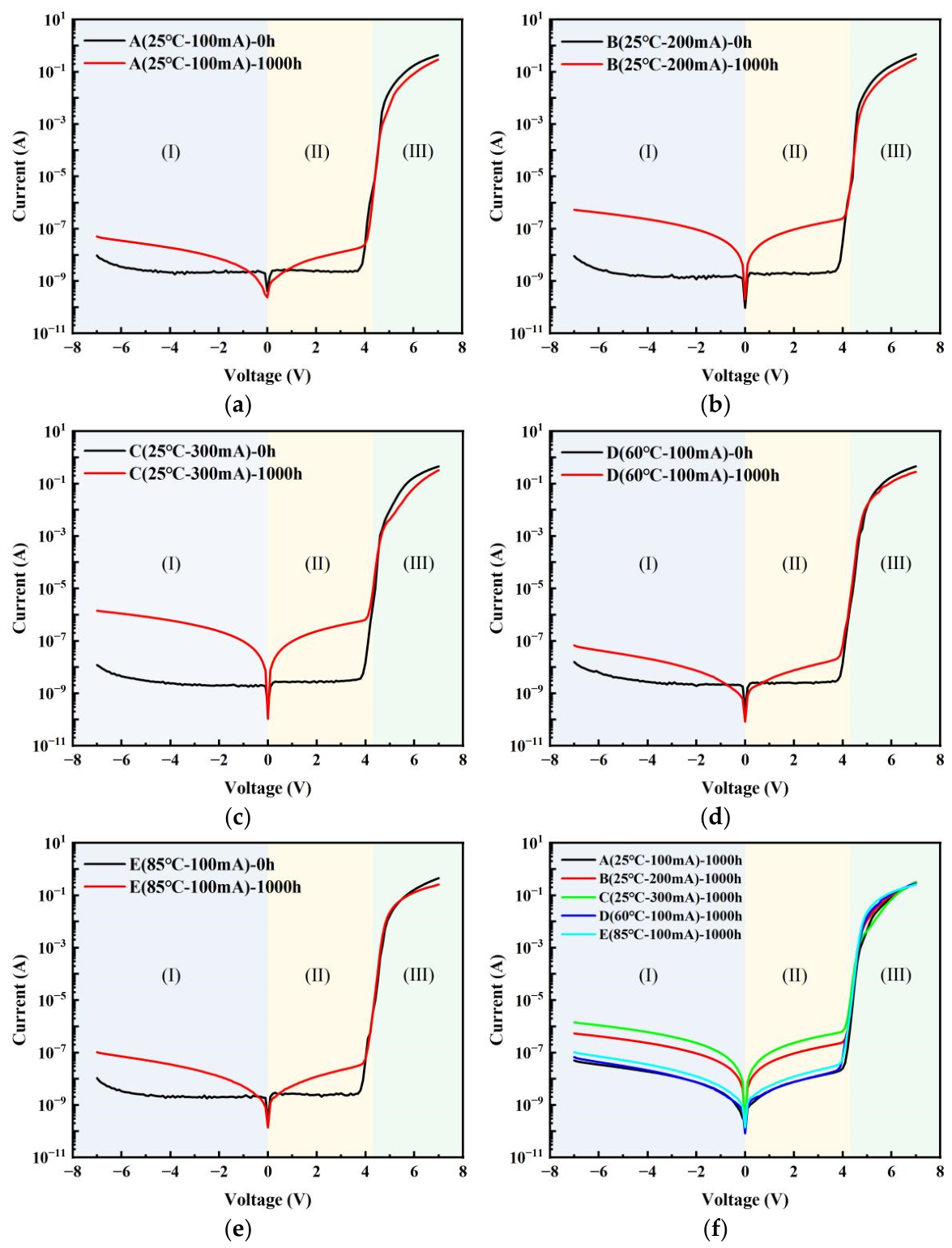
To further clarify the physical mechanism of device degradation, Figure 4 presents the I-V curves of the samples before and after a 1000 h aging test under various stress conditions. Figure 4f summarizes and compares the I-V curves of all sample groups after 1000 h of aging. The I-V curves can be divided into three regions: (I) the reverse bias region; (II) the region below the turn-on voltage (0~4.7 V); (III) the region above the turn-on voltage (>4.7 V). Table 2 lists the leakage current values at −3 V and 3 V before and after aging to quantitatively analyze the influence of different aging conditions on the leakage current.
The initial leakage current values (0 h) of all samples are largely consistent. Thus, the leakage currents after aging tests are mainly compared. Taking the current at −3 V as an example, the leakage current of sample A increases from 2.06 × 10⁻⁹ A to 1.28 × 10⁻⁸ A after the 1000 h aging test, increasing by nearly one order of magnitude. The leakage currents of samples B and C with increased aging current rise to 1.57 × 10⁻⁷ A and 4.03 × 10⁻⁷ A, increasing by approximately two orders of magnitude. The leakage currents of samples D and E with elevated aging temperature increase to 1.35 × 10⁻⁸ A and 2.26 × 10⁻⁸ A, showing only a slight increase compared with sample A. At a constant temperature of 25 °C, a higher aging current results in a larger leakage current in regions I and II after 1000 h of aging. At a constant current of 100 mA, the leakage current increases with rising aging temperature. However, both the I–V curves and the data in Table 2 show that thermal stress has a much weaker effect on leakage current than electrical stress, which perfectly corresponds to the optical power degradation shown in Figure 3. It also confirms that the active materials exhibit relatively good stability under combined electrical and thermal stress, as the degree of degradation remains far below that induced by the intensified electrical stress. Meanwhile, the results in region III indicate that the current of all sample groups has decreased to varying degrees after the 1000 h aging test.
Previous studies [19,21] have shown that the reverse leakage current in region I is related to trap-assisted tunneling, and the forward leakage current in region II is attributed to parasitic carrier leakage channels. However, I–V characteristic analysis shows that the current values of all samples at −3 V and 3 V are almost the same after the 1000 h aging test. Therefore, we consider that the leakage currents in regions I and II are affected by the combined action of these two mechanisms. Based on the electrical characteristic analysis and relevant studies, we infer that electrical stress induces the activation and generation of point defects near the active region, and carriers cross the junction barrier through deep-level defect states in a multi-step hopping manner [22,23]. Meanwhile, the number of dislocations near the active region may increase, forming low-resistance ohmic bypasses that allow carriers to transport around the barrier directly [24,25]. These defects act as non-radiative recombination centers, reduce the radiative recombination efficiency, and result in a decline in LOP. The increase in forward voltage in region III is mainly attributed to the increase in series resistance. This is the result of continuous degradation of the device’s internal structure by electrical stress, leading to defect proliferation and increased heat generation. The elevated forward voltage further enhances the internal electric field, thereby exacerbating defect proliferation. This is the key reason why electrical stress causes more severe degradation than thermal stress.

3.3. Thermal Properties

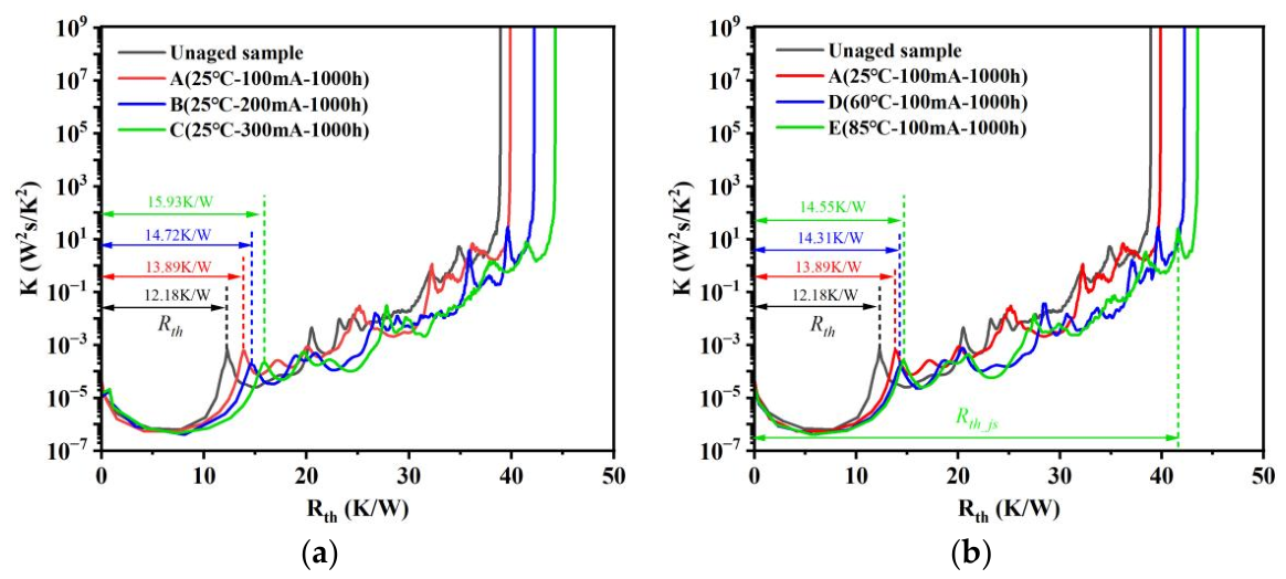
For DUV LEDs, thermal accumulation is the core factor inducing irreversible performance degradation and even catastrophic failure of devices. Thermal resistance measurement is a critical characterization method in reliability research. The dynamic evolution of thermal resistance can provide quantitative experimental evidence for microscopic failure behaviors, such as dislocation multiplication, interface degradation and defect accumulation. The transient thermal characteristics of different samples were measured using a T3Ster thermal resistance test system, as shown in Figure 5. The test current was set to 100 mA, the heating time to 60 s, and the tests were conducted in accordance with the JESD51-14 standard, with data analysis performed using the Transient Thermal Analysis (TTA) method.
To highlight the effect of aging stress, the unaged samples were also tested. At a driving current of 100 mA, the chip thermal resistance (Rth) of the unaged sample is 12.18 K/W, and the Rth values of samples A, B, and C are 13.89 K/W, 14.72 K/W, and 15.93 K/W, respectively. As shown in Figure 5b, the Rth values of samples D and E are 14.31 K/W and 14.55 K/W, which are very close to that of sample A. The results show that the influence of electrical stress on Rth is much greater than that of thermal stress. From these results, we infer that the increase in chip thermal resistance is mainly attributed to point defects and electron leakage induced by electrical stress. On the one hand, carriers in the high-electric-field region gain sufficient energy to induce impact ionization, which breaks covalent bonds and generates a large number of point defects. On the other hand, the increased defect density in the p-EBL weakens its electron blocking capability, causing a large number of electrons to leak into the p-type layer through the p-EBL. These leaked electrons generate Joule heat via non-radiative recombination in the p-type layer, which is manifested as an increase in thermal resistance. In contrast, thermal stress only reduces the heat dissipation capacity of the device and has little effect on thermal resistance.

3.4. Lifetime Prediction

To quantitatively evaluate the service life of devices under rated operating conditions and shorten the evaluation cycle, it is necessary to conduct lifetime prediction research on AlGaN-based DUV LEDs. According to the different stress conditions in the accelerated aging tests, the inverse power law model and the Arrhenius model are adopted to predict the lifetime of AlGaN-based DUV LEDs. The time when the LOP drops to 70% of the initial value is defined as the effective lifetime of each LED, which is compared with the actual lifetime to verify the accuracy of the adopted models.
The inverse power law model is selected as the lifetime prediction model when current, voltage, or mechanical stress is adopted as the aging test condition [26], and its expression is given as follows:
t   =   C 0 I n
where t is the effective life under the accelerated aging test current, C0 and n are fitting parameters, and I is the magnitude of the applied electrical stress.
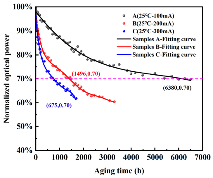
The inverse power law model corresponds to the electrical test group; by substituting the corresponding parameters for samples B and C into Equation (1), C0 and n can be obtained. Figure 6 shows the variation curves of the normalized LOP of the samples under three different aging currents with aging time. Firstly, the effective lifetimes of samples A, B, and C are fitted by the least square method, which are 6380 h, 1496 h, and 675 h, respectively. Then, the current and effective lifetime data (I, t) of samples B and C, (0.2, 1496) and (0.3, 675), are substituted into Equation (1), and the fitting parameters C0 and n are calculated to be 63.53 and 1.96, respectively. Finally, the normal operating current of 100 mA is substituted into Equation (1), the predicted lifetime of the sample at 100 mA was calculated to be 5832 h, with an error of 8.59% between the predicted and the actual measured value (6380 h).
The Arrhenius model, proposed by the distinguished Swedish physical chemist Arrhenius in 1889, provides the theoretical foundation for LED temperature-stress accelerated life testing and helps extrapolate product lifetimes under normal stress conditions [27]. The equation is as follows:
t   =   A 0 e E a k T j
where t is the effective lifetime under a specific stress condition, A0 is a constant, Ea denotes the activation energy of a certain failure mechanism, k is the Boltzmann constant (8.617 × 10⁻⁵ eV/K), and Tj represents the junction temperature.
The junction temperature Tj of the DUV LED chip can be calculated by the following equation [28]:
T j =   T x + I F V F R t h j x
where Tx is the reference temperature of the device under test in the preset ambient environment, IF and VF are the operating current and voltage, respectively, and Rth-jx is the thermal resistance from the PN junction to the ambient of the device, which can be obtained from Figure 5.
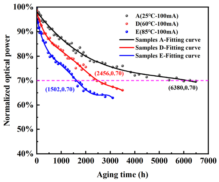
The Arrhenius model is employed for the thermo-electric combined stress test group, and the corresponding parameters of samples D and E are substituted into Equation (2) to obtain the constants A0 and Ea. From Figure 5, the junction-to-ambient thermal resistances Rth-jx for samples A, D, and E are 36.12 K/W, 39.84 K/W, and 41.52 K/W, respectively. Substituting Rth-jx into Equation (3), the junction temperatures Tj for samples A, D, and E are calculated to be 316.57 K, 353.46 K, and 379.32 K, respectively. Figure 7 shows the curves of normalized LOP versus aging time for the samples under the three aging temperatures. Substituting the Tj and t values for samples D (353.46 K, 2456 h) and E (379.32 K, 1502 h) into Equation (2) to calculate A0 and Ea, the results are A0 = 1.81 and Ea = 0.220 eV. Substituting the normal operating junction temperature of 316.57 K into Equation (2), the predicted lifetime of the DUV LED at 25°C is calculated to be 5724 h. The error between this predicted lifetime and the measured lifetime is 10.28%.
Comparative analysis reveals that the inverse power law model exhibits better agreement with the measured L70 lifetime, which is mainly affected by the degradation mechanism and the input variables of the model. On the one hand, device degradation is dominated by electrical stress, and the inverse power law model is precisely a prediction model based on electrical stress variations. On the other hand, the Arrhenius model relies on an indirectly calculated junction temperature with inherent measurement errors. Moreover, changes in interfacial thermal resistance during aging further increase the uncertainty in junction temperature estimation. Therefore, to ensure prediction accuracy, the inverse power law model is preferred for lifetime prediction of AlGaN-based DUV LEDs.

4. Conclusions

In summary, AlGaN-based DUV LEDs with a center emission wavelength of 270 nm are subjected to accelerated aging stress tests. By analyzing the variations in LOP, I-V characteristics, and thermal resistance during the aging process, it is determined that electrical stress is the primary factor contributing to device performance degradation, while thermal stress plays only a secondary role. Higher electrical stress results in faster LOP decay with an initial rapid drop and subsequent slow decline, and thermal stress has a much weaker effect on LOP than electrical stress. I-V characterization results show that the leakage current increases significantly with rising electrical stress, while thermal stress has a negligible effect on the leakage current. The forward and reverse leakage currents are jointly governed by trap-assisted tunneling and parasitic carrier leakage channels. Thermal resistance measurements confirm that the increased chip thermal resistance mainly arises from point defects and electron leakage induced by electrical stress. In addition, the effective device lifetimes predicted by the inverse power law model and the Arrhenius model are 5832 h and 5724 h, respectively. Compared with the measured lifetime of 6380 h, the inverse power law model exhibits higher prediction accuracy. This work will provide a robust theoretical foundation for improving the reliability and extending the service life of AlGaN-based DUV LEDs.

Author Contributions

Conceptualization, S.X., M.G., X.S. and N.L.; methodology, S.X. and X.S.; validation, S.X.; formal analysis, S.X., M.G. and X.S.; investigation, M.G., X.S. and T.Z.; resources, X.S., N.L. and T.L.; data curation, S.X.; writing—original draft preparation, S.X.; writing—review and editing, X.S.; supervision, T.L. and J.L.; project administration, N.L. and J.L.; funding acquisition, N.L. and J.L. All authors have read and agreed to the published version of the manuscript.

Funding

This work was supported by the Key R&D Project of Shanxi Province (Grant No. 202302030201005), the Open Fund Project of the State Key Laboratory of Widegap Semiconductor Optoelectronic Materials and Technologies (No. SOMAT-2025-03), and the National Key R&D Program of China (Grant No. 2022YFB3604804).

Institutional Review Board Statement

Not applicable.

Informed Consent Statement

Not applicable.

Data Availability Statement

Data are contained within the article.

Acknowledgments

The authors wish to thank the sponsorship provided by the Institute of Semiconductors, Chinese Academy of Sciences, and Shanxi Zhongke Lu’an Ultraviolet Optoelectronics Technology Co., Ltd.

Conflicts of Interest

Jimin Li and Tong Zhang are employed by Shanxi Zhongke Lu’an Ultraviolet Optoelectronics Technology Co., Ltd. The remaining authors declare that the research was conducted in the absence of any commercial or financial relationships that could be construed as a potential conflict of interest.

References

  1. Chen, Y.; Ben, J.; Xu, F.; Li, J.; Chen, Y.; Sun, X.; Li, D. Review on the Progress of AlGaN-based Ultraviolet Light-Emitting Diodes. Fundam. Res. 2021, 1, 717–734. [Google Scholar] [CrossRef] [Scilit]
  2. Xu, R.; Kang, Q.; Zhang, Y.; Zhang, X.; Zhang, Z. Research Progress of AlGaN-Based Deep Ultraviolet Light-Emitting Diodes. Micromachines 2023, 14, 844. [Google Scholar] [CrossRef] [Scilit]
  3. Li, D.; Jiang, K.; Sun, X.; Guo, C. AlGaN photonics: Recent advances in materials and ultraviolet devices. Adv. Opt. Photonics 2018, 10, 43–110. [Google Scholar] [CrossRef] [Scilit]
  4. Kneissl, M.; Seong, T.-Y.; Han, J.; Amano, H. The emergence and prospects of deep-ultraviolet light-emitting diode technologies. Nat. Photonics 2019, 13, 233–244. [Google Scholar] [CrossRef] [Scilit]
  5. Zhou, S.; Liao, Z.; Sun, K.; Zhang, Z.; Qian, Y.; Liu, P.; Du, P.; Jiang, J.; Lv, Z.; Qi, S. High-Power AlGaN-Based Ultrathin Tunneling Junction Deep Ultraviolet Light-Emitting Diodes. Laser Photonics Rev. 2023, 18, 2300464. [Google Scholar] [CrossRef] [Scilit]
  6. Takamure, K.; Iwatani, Y.; Amano, H.; Yagi, T.; Uchiyama, T. Inactivation characteristics of a 280 nm Deep-UV irradiation dose on aerosolized SARS-CoV-2. Environ. Int. 2023, 177, 108022. [Google Scholar] [CrossRef] [Scilit] [PubMed]
  7. Gupta, H.; Ahmad, S.; Kattayat, S.; Kumar, D.; Dalela, S.; Siddiqui, M.J.; Alvi, P.A. Improvement in efficiency and luminous power of AlGaN-based D-UV LEDs by using partially graded quantum barriers. Superlattices Microstruct. 2020, 142, 106543. [Google Scholar] [CrossRef] [Scilit]
  8. Hao, L.; Wang, L.; Guo, Y.; Sun, X.-J.; Guo, K.; Shen, C.; Zhang, T.; Zhang, X.; Wang, S.; Jia, X.; et al. Enhancing the Performance for High-Power AlGaN-Based Deep Ultraviolet Light-Emitting Diodes Using Self-Assembled Chip-Scale Inclined Sidewall. IEEE Electron Device Lett. 2025, 46, 377–380. [Google Scholar] [CrossRef] [Scilit]
  9. Qiu, H.; Wang, L.; Guo, Y.; Guo, K.; Zhang, X.; Jia, X.; Shen, C.; Zhang, T.; Sun, X.-J.; Wei, X.; et al. Enhancing the light output power of deep ultraviolet light-emitting diodes with a ultra-thin p-type layer through etching non-ohmic contact p-GaN region. J. Appl. Phys. 2025, 138, 145702. [Google Scholar] [CrossRef] [Scilit]
  10. Hao, J.; Ke, H.-L.; Jing, L.; Sun, Q.; Sun, R.-T. Prediction of lifetime by lumen degradation and color shift for LED lamps, in a non-accelerated reliability test over 20,000  h. Appl. Opt. 2019, 58, 1855–1861. [Google Scholar] [CrossRef] [Scilit] [PubMed]
  11. Padmasali, A.N.; Kini, S.G. Accelerated Testing Based Lifetime Performance Evaluation of LEDs in LED Luminaire Systems. IEEE Access 2021, 9, 137140–137147. [Google Scholar] [CrossRef] [Scilit]
  12. Piva, F.; De Santi, C.; Deki, M.; Kushimoto, M.; Amano, H.; Tomozawa, H.; Shibata, N.; Meneghesso, G.; Zanoni, E.; Meneghini, M. Stability and degradation of AlGaN-based UV-B LEDs: Role of doping and semiconductor defects. Microelectron. Reliab. 2019, 100–101, 113418. [Google Scholar] [CrossRef] [Scilit]
  13. Piva, F.; De Santi, C.; Deki, M.; Kushimoto, M.; Amano, H.; Tomozawa, H.; Shibata, N.; Meneghesso, G.; Zanoni, E.; Meneghini, M. Modeling the degradation mechanisms of AlGaN-based UV-C LEDs: From injection efficiency to mid-gap state generation. Photonics Res. 2020, 8, 1786–1791. [Google Scholar] [CrossRef] [Scilit]
  14. Park, T.H.; Son, K.R.; Hirayama, H.; Kim, T.G. High-Efficiency and High-Reliability Deep-UV Light-Emitting Diodes Using Transparent Ni-Implanted AlN Ohmic Electrodes. IEEE Access 2021, 9, 166617–166623. [Google Scholar] [CrossRef] [Scilit]
  15. Chen, Y.; Lv, Q.; Liu, J.; Huang, X.; Cao, Y.; Yang, T.; Mi, T.; Wang, X.; Liu, J. Mitigating current crowding for enhanced reliability of AlGaN-based deep-ultraviolet LEDs through triangular island-shaped p-electrode design. Opt. Laser Technol. 2025, 181, 112026. [Google Scholar] [CrossRef] [Scilit]
  16. Ruschel, J.; Glaab, J.; Beidoun, B.; Ploch, N.L.; Rass, J.; Kolbe, T.; Knauer, A.; Weyers, M.; Einfeldt, S.; Kneissl, M. Current-induced degradation and lifetime prediction of 310  nm ultraviolet light-emitting diodes. Photonics Res. 2019, 7, B36–B40. [Google Scholar] [CrossRef] [Scilit]
  17. Zhang, J.; Gao, Y.; Zhou, L.; Lunev, A.; Wu, S.; Zhang, B.; Khan, A. Thermal droop investigations on ultraviolet C-band light-emitting diodes. Appl. Phys. Lett. 2025, 127, 193302. [Google Scholar] [CrossRef] [Scilit]
  18. Shen, C.-H.; Yang, R.-L.; Gong, H.-L.; Zhu, L.-H.; Gao, Y.-L.; Chen, G.-L.; Chen, Z.; Lu, Y.-j. Optical power degradation mechanisms in 271 nm AlGaN-based deep ultraviolet light-emitting diodes. Opt. Express 2023, 31, 20265–20273. [Google Scholar] [CrossRef] [Scilit]
  19. Monti, D.; De Santi, C.; Da Ruos, S.; Piva, F.; Glaab, J.; Rass, J.; Einfeldt, S.; Mehnke, F.; Enslin, J.; Wernicke, T.; et al. High-Current Stress of UV-B (In)AlGaN-Based LEDs: Defect-Generation and Diffusion Processes. IEEE Trans. Electron Devices 2019, 66, 3387–3392. [Google Scholar] [CrossRef] [Scilit]
  20. Ma, Z.; Cao, H.; Lin, S.; Li, X.; Zhao, L. Degradation and failure mechanism of AlGaN-based UVC-LEDs. Solid-State Electron. 2019, 156, 92–96. [Google Scholar] [CrossRef] [Scilit]
  21. Trivellin, N.; Monti, D.; De Santi, C.; Buffolo, M.; Meneghesso, G.; Zanoni, E.; Meneghini, M. Current induced degradation study on state of the art DUV LEDs. Microelectron. Reliab. 2018, 88–90, 868–872. [Google Scholar] [CrossRef] [Scilit]
  22. Wang, Y.-Z.; Wang, M.-S.; Hua, N.; Chen, K.; He, Z.-M.; Zheng, X.-F.; Li, P.-X.; Ma, X.-H.; Guo, L.-X.; Hao, Y. Effects of electrical stress on the characteristics and defect behaviors in GaN-based near-ultraviolet light emitting diodes. Chin. Phys. B 2022, 31, 068101. [Google Scholar] [CrossRef] [Scilit]
  23. Su, M.; Liu, H. Effect of Trap Behavior on Recombination in AlGaN-Based UV-C LEDs Degradation. IEEE Trans. Electron Devices 2024, 71, 1974–1979. [Google Scholar] [CrossRef] [Scilit]
  24. Ma, Z.; Almalki, A.; Yang, X.; Wu, X.; Xi, X.; Li, J.; Lin, S.; Li, X.; Alotaibi, S.; Al huwayz, M.; et al. The influence of point defects on AlGaN-based deep ultraviolet LEDs. J. Alloys Compd. 2020, 845, 156177. [Google Scholar] [CrossRef] [Scilit]
  25. Islam, Z.; Haque, A.; Glavin, N. Real-time visualization of GaN/AlGaN high electron mobility transistor failure at off-state. Appl. Phys. Lett. 2018, 113, 183102. [Google Scholar] [CrossRef] [Scilit]
  26. Abdul Majid, M.; Helal, S.; Kittaneh, O. On the inverse power law-normal model for life prediction of organic light emitting diodes. Qual. Reliab. Eng. Int. 2023, 39, 2677–2685. [Google Scholar] [CrossRef] [Scilit]
  27. Arques-Orobon, F.J.; Vazquez, M.; Nuñez, N. Lifetime Analysis of Commercial 3 W UV-A LED. Crystals 2020, 10, 1083. [Google Scholar] [CrossRef] [Scilit]
  28. Xi, Y.; Schubert, E.F. Junction–temperature measurement in GaN ultraviolet light-emitting diodes using diode forward voltage method. Appl. Phys. Lett. 2004, 85, 2163–2165. [Google Scholar] [CrossRef] [Scilit]
Figure 1. (a) Epitaxial structure diagram and (b) microscope image of DUV LEDs. The regions outlined by the blue dashed lines represent the deep trenches etched down to the n-AlGaN layer.
Coatings 16 00597 g001
Figure 2. The LOP and WPE of the LED before aging test at various currents.
Coatings 16 00597 g002
Figure 3. (a) LOP and (b) normalized LOP for the electrical stress test group, and (c) LOP and (d) normalized LOP for the thermo–electrical composite stress test group.
Coatings 16 00597 g003
Figure 4. The current–voltage (I–V) characteristics (semi-logarithmic scale) of the 270 nm DUV LEDs measured before and after the aging tests. (a) Sample A, (b) sample B, (c) sample C, (d) sample D, (e) sample E, and (f) comparison of all samples.
Coatings 16 00597 g004
Figure 5. The transient thermal characteristics of the 270 nm DUV LEDs measured before and after the aging tests. (a) Electrical stress test group and (b) thermo–electrical composite stress test group.
Coatings 16 00597 g005
Figure 6. Curves of normalized optical power versus aging time under different aging currents.
Coatings 16 00597 g006
Figure 7. Curves of normalized optical power versus aging time at different aging temperatures.
Coatings 16 00597 g007
Table 1. Experimental arrangement of different aging samples.
Aging TestAging Current (mA)Aging Temperature (°C)Operation Time (h)
Samples A100256500
Samples B200253300
Samples C300251700
Samples D100603500
Samples E100853100
Table 2. The leakage current at −3 V and 3 V of the LED samples before and after the stress.
Aging TestLeakage Current at −3 V Bias (A)Leakage Current at 3 V Bias (A)
0 h1000 h0 h1000 h
Samples A2.06 × 10−91.28 × 10−82.32 × 10−91.27 × 10⁻⁸
Samples B1.74 × 10−91.57 × 10−71.98 × 10−91.56 × 10⁻⁷
Samples C2.23 × 10−94.03 × 10−72.95 × 10−94.01 × 10⁻⁷
Samples D2.27 × 10−91.35 × 10−82.54 × 10−91.33 × 10⁻⁸
Samples E2.01 × 10−92.26 × 10−82.81 × 10−92.16 × 10⁻⁸
Disclaimer/Publisher’s Note: The statements, opinions and data contained in all publications are solely those of the individual author(s) and contributor(s) and not of MDPI and/or the editor(s). MDPI and/or the editor(s) disclaim responsibility for any injury to people or property resulting from any ideas, methods, instructions or products referred to in the content.