Article

Understanding the Chamber Wall-Deposited Thin Film of Plasma Deposition Equipment for the Efficiency of In Situ Dry-Cleaning

Department of Semiconductor Engineering, Myongji University, Yongin-si 17058, Republic of Korea
*
Author to whom correspondence should be addressed.
Coatings 2025, 15(5), 563; https://doi.org/10.3390/coatings15050563
Submission received: 4 April 2025 / Revised: 30 April 2025 / Accepted: 7 May 2025 / Published: 8 May 2025

Abstract

:
In plasma-enhanced chemical vapor deposition (PECVD) processes, thin films can accumulate on the inner chamber walls, resulting in particle contamination and process drift. In this study, we investigate the physical and chemical properties of these wall-deposited films to understand their spatial variation and impact on chamber maintenance. A 6-inch capacitively coupled plasma (CCP)-type PECVD system was used to deposit SiO2 films, whilst long silicon coupons were attached vertically to the chamber side walls to collect contamination samples. The collected contamination samples were comparatively analyzed in terms of their chemical properties and surface morphology. The results reveal significant differences in hydrogen content and Si–O bonding configurations compared to reference films deposited on wafers. The top chamber wall, located near the plasma region, exhibited higher hydrogen incorporation and larger Si–O–Si bonding angles, while the bottom wall exhibited rougher surfaces with larger particulate agglomerates. These variations were closely linked to differences in gas flow dynamics, precursor distribution, and the energy state of the plasma species at different chamber heights. The findings indicate that top-wall contaminants are more readily cleaned due to their high hydrogen content, while bottom-wall residues may be more persistent and pose higher risks for particle generation. This study provides insights into wall contamination behavior in PECVD systems and suggests strategies for spatially optimized chamber cleaning and conditioning in high-throughput semiconductor processes.

1. Introduction

As semiconductor device scaling continues, the sensitivity to process variability and particle contamination becomes increasingly critical [1]. Chemical vapor deposition (CVD) is a highly versatile technique widely utilized for the fabrication of a diverse range of materials, including graphene, conducting polymers, inorganic semiconductors, and metal oxides [2,3]. This adaptability makes CVD a critical technology for next-generation device manufacturing. One of them, PECVD, is widely used for forming dielectric layers at low-temperatures [4,5]. However, during PECVD, unwanted byproducts can accumulate not only on the wafer but also on internal chamber surfaces such as walls and electrodes. These contaminants can act as sources of particles [6], alter chamber impedance [7], and degrade process reproducibility [8,9,10]. To address this, in situ dry-cleaning (ISD) processes using fluorine-based chemistries (e.g., NF3, SF6) are commonly employed between deposition steps to remove contaminants without exposing the chamber to atmosphere [11,12]. Despite their effectiveness, excessive cleaning can erode protective coatings on chamber components, leading to increased particle generation and hardware degradation [13]. Hence, precise control of the ISD process is essential for maintaining chamber stability and minimizing downtime [14].
Previous studies have proposed endpoint detection (EPD) methods based on monitoring signals from uniformly deposited films [15,16]. However, they have overlooked the actual state of contamination on chamber walls where deposition environments differ significantly in temperature, gas composition, and plasma proximity compared to the wafer surface [17]. Also, while previous studies about wall contamination have investigated the formation of chamber wall contaminants through experimental modeling or indirect monitoring methods in plasma systems [18,19], few have specifically addressed the chemical composition and bonding structure of wall-deposited films considering their spatial variation along the vertical axis. Wall contamination is expected to vary spatially along the vertical axis due to differences in gas flow dynamics and plasma exposure.
Although the side-wall-deposited films are not intended for direct device integration and their properties critically influence process stability, plasma uniformity, and particle generation in semiconductor manufacturing. Understanding the composition, bonding structure, and morphology of side-wall-deposited films (referred to here as “wall contaminants”) is crucial not only for evaluating their potential to induce process drift [20,21,22,23], but also for improving ISD effectiveness. These wall contaminants differ in formation mechanisms and cleaning behavior from films deposited on wafers, and thus merit dedicated analysis.
In this study, we investigate the spatial variation in the properties of contaminant films formed on the inner walls of a PECVD chamber. Using surface-sensitive techniques, such as X-ray photoelectron spectroscopy (XPS), Fourier-transform infrared spectroscopy (FT-IR), atomic force microscopy (AFM), and scanning electron microscopy (SEM), we analyze the composition and morphology of these films at different vertical locations. Our goal is to reveal how these variations correlate with cleaning behavior, thereby providing a foundation for improved ISD process control and chamber management in PECVD systems.

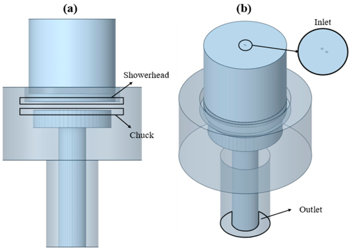
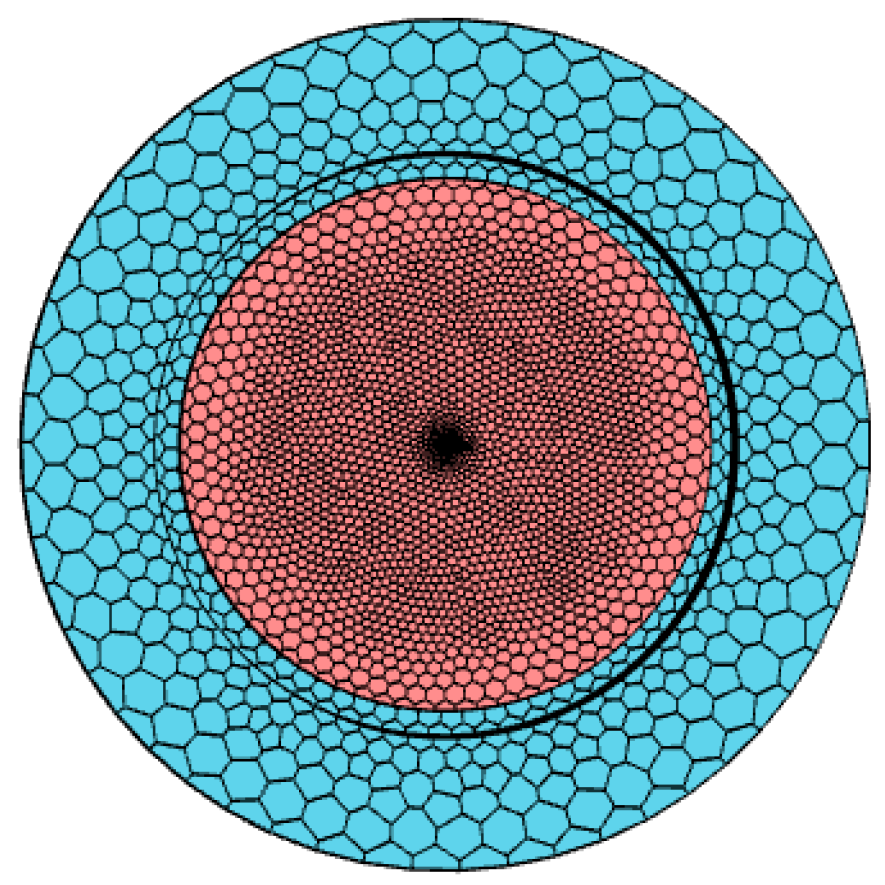
2. Simulation Method

Computational fluid dynamics (CFDs) simulation was employed to analyze the gas flow along the chamber wall. The 6-inch PECVD system was modeled using ANSYS SpaceClaim 2022 R2 and is depicted in Figure 1. The inlet consists of two gas lines, each 1.5 mm in diameter. The outlet has a diameter of 120 mm and a central column measuring 63.7 mm in diameter, forming an annular pathway for gas flow. Figure 2 illustrates the structure of the showerhead, which is composed of nozzles with a diameter of 0.84 mm arranged at intervals of 12.7 mm. The gap between the showerhead and the chuck, which has a diameter of 180 mm, is 20 mm. The mesh design was generated using ANSYS Fluent Meshing 2022 R2. The vertical alignment of the gas inlet and outlet reflects the actual configuration of the 6-inch CCP-type PECVD system used in this study. While this specific geometry was modeled, the simulation approach is not limited to vertically aligned reactors and can be extended to systems with different inlet–outlet geometries. The cell size progressively increased from 0.3 mm at the smallest inlet to 30 mm, as shown in Figure 3. The simulation was conducted using ANSYS Fluent 2022 R2, with boundary conditions configured to match the experimental conditions, as detailed in Table I. The inlet velocity was calculated based on a total gas flow of 46 sccm through two 1.5 mm-diameter inlets, resulting in an average velocity of ~2.3 m/s. The outlet pressure was fixed at 500 mTorr. The process temperature was set to 300 °C. Physical properties of each gas were input based on standard values. The gases used in the CFDs simulations (SiH4, N2O, and Ar) shown in Table 1 correspond to the actual process gases employed during PECVD. Given wall reactions are distant from the complex chemical processes occurring in the plasma bulk, and that the primary objective of this study is to investigate the gas flow behavior along the chamber walls in relation to the showerhead and chamber structure, chemical reactions were intentionally excluded from the simulation. The simulation instead focused solely on the temperature and flow rate conditions of the fluid.

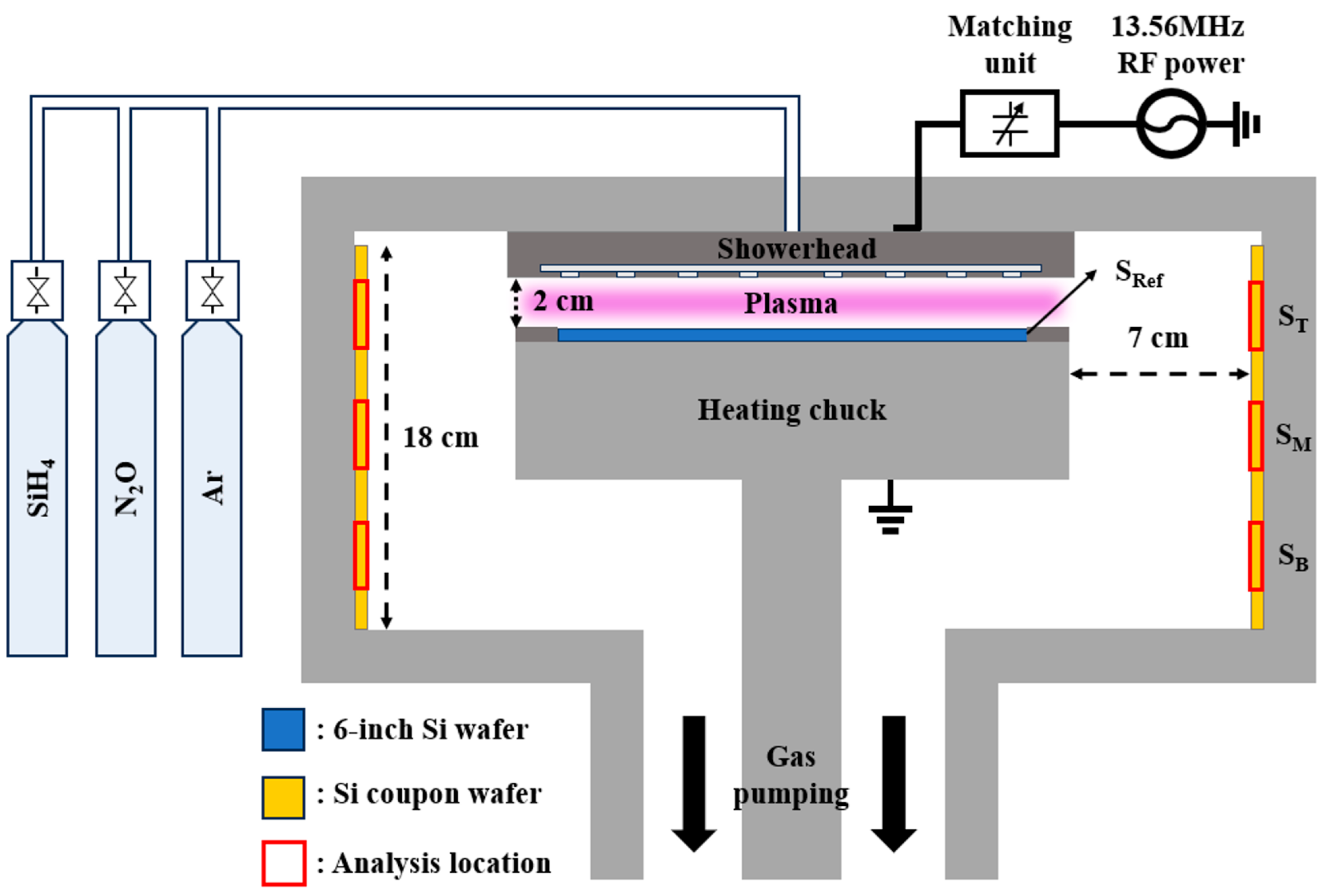
3. Experimental Methods

For the experiment to fabricate the chamber wall-accumulated thin film, we employed a 6-inch CCP type PECVD system powered by 13.56 MHz in frequency. Chamber wall contaminated surface samples were obtained by attaching coupon wafers to the chamber side wall by conducting repeated deposition processes, as illustrated in Figure 4. Coupon wafers were directly attached to the chamber walls using double-sided carbon adhesive tape to minimize interference and ensure that they experienced deposition conditions comparable to those of the native chamber surface. It should be noted that the distances from the plasma, gas chemical compositions, and temperatures may vary depending on the vertical location of chamber wall. To account for the differences in contamination levels, long-rectangular-cut silicon coupons, with dimensions of 1 cm by 18 cm, were attached to the side wall.
The objective of the experiment was to understand the properties of the contaminants, whose material forming mechanism is plasma diffusion, accumulated through continuous deposition runs on the chamber walls. Continuous deposition runs were carried out to contaminate the chamber walls, resulting in a contamination film thickness of approximately 70 nm. Silane-based recipes, such as those shown in Table 2, are widely used for the PECVD of SiO2 thin films because they enable high deposition rates while maintaining film quality at low substrate temperatures [1]. We used the silane-based SiO2 deposition recipe, as presented in Table 2, to investigate the occurrence of wall contamination during the actual deposition process. Additionally, to serve as a reference, a 6-inch full wafer was placed on the chuck to obtain a deposition film with direct plasma. The contaminants were then analyzed at three points on the wall surface, as is already indicated in Figure 4, which are presented as ST, SM, and SB. To facilitate discussion, the sample positions are designated as SRef for the reference chuck sample, and ST, SM, and SB for the top, middle, and bottom wall samples, respectively. In addition, thermal tapes were attached at each sampling position to measure the temperature along the chamber wall.
The thickness of the obtained contamination film is measured using a reflectometer (ST-2000, KMAC Co., Ltd., Daejeon, Republic of Korea). It allows for the observation of the differences in contamination levels across wall positions. To identify the chemical composition of the contamination film, X-ray photoelectron spectroscopy (XPS) is employed, using an Al-Kα (1486.6 eV) X-ray source. The XPS energy calibration was performed based on the C 1s peak at 284.6 eV, as reported in previous studies, and cross-verification was conducted using the O 1s peak at 532.6 eV in consideration of the known limitations of C 1s referencing [24]. The XPS data were analyzed using Gaussian deconvolution to resolve detailed binding states. Quantitative analysis was conducted based on the integrated areas of the deconvoluted peaks. Fourier transform infrared spectroscopy (FT-IR, IRTrancer-100, Simadzu, Japan) is used to identify the bonding structure. Furthermore, scanning electron microscopy (SEM, Scios2 from FEI Co., Hillsborough, OR, USA) is employed to observe the surface particle structure of the contamination film. Atomic force microscopy (AFM), manufactured by Anton Paar, is used to measure a 15 by 15 μm area of the film for surface roughness and 3D surface structure observation.

4. Results and Discussion

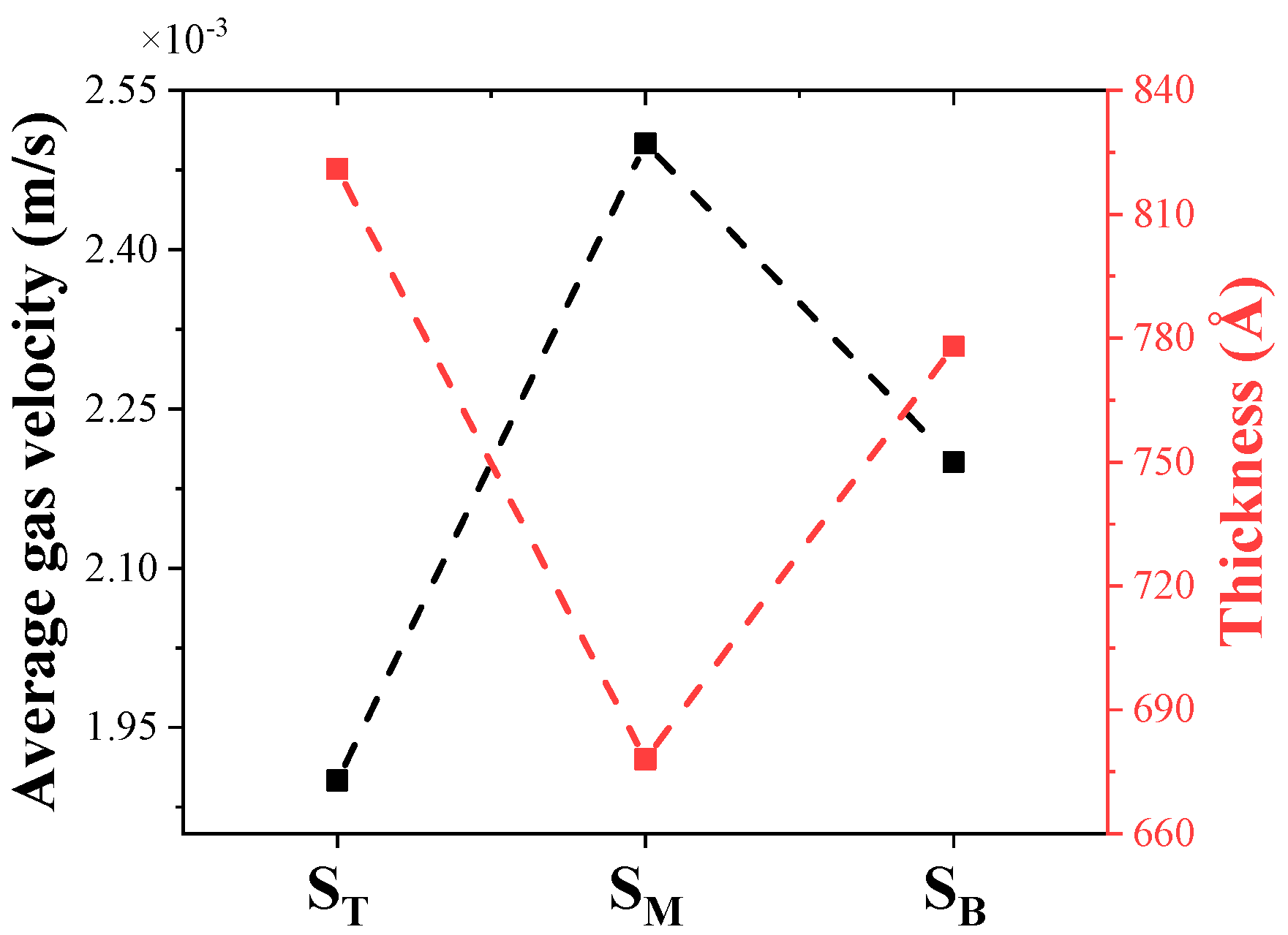
4.1. Thickness Distribution and Gas Flow Dynamics

The contamination thickness on the plasma deposition chamber walls was measured at different positions to compare contamination levels. The average deposition rate of the PECVD equipment was approximately 80 Å/min. Considering process stability, the observed deposition rate (~80 Å/min) falls within the typical range reported for the PECVD of SiO2 films [25]. Continuous deposition experiments resulted in a wall contamination layer with an average thickness of 700 Å. The measured thickness of the reference substrate (SRef, deposited on the chuck) was 108,100 Å, indicating a deposition rate difference of approximately 154 times compared to deposition runs without chamber cleaning.
To evaluate the spatial distribution of contamination on the chamber walls, film thicknesses were measured at the three vertical positions of top (ST), middle (SM), and bottom (SB). As shown in Figure 5, the measured thicknesses were approximately 780 Å at ST, 690 Å at SB, and 660 Å at SM. This indicates that the top wall, located near the plasma region, exhibited the highest contamination, followed by the bottom and then the middle region. Gas flow simulation results revealed that the average gas velocity was lowest at ST and SB, and highest at SM, which suggests that shorter residence time at SM led to lower precursor reaction rates, and thus lower contamination. This inverse correlation between contamination level and gas velocity implies that the middle wall region may be more easily cleaned during ISD cycles.

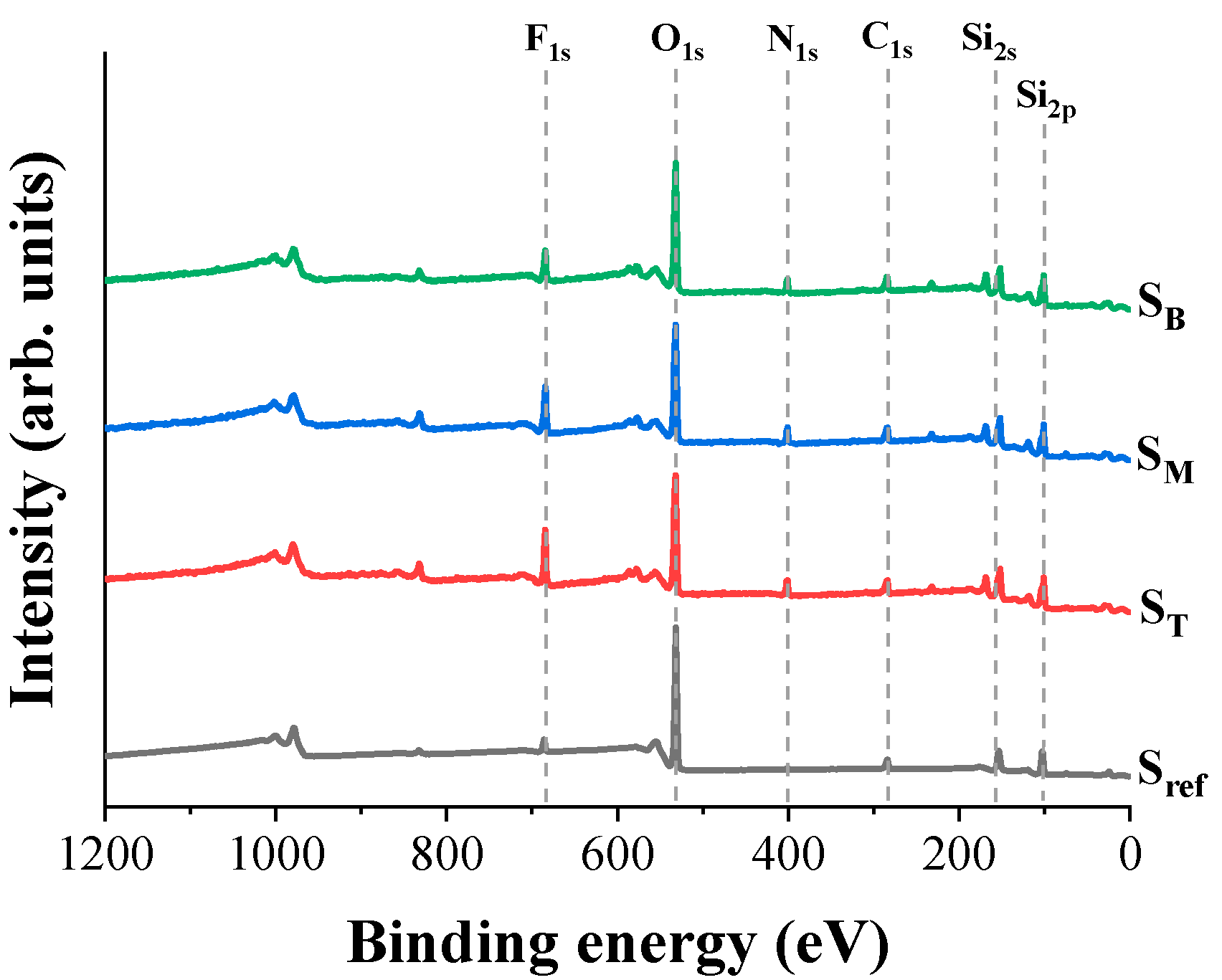
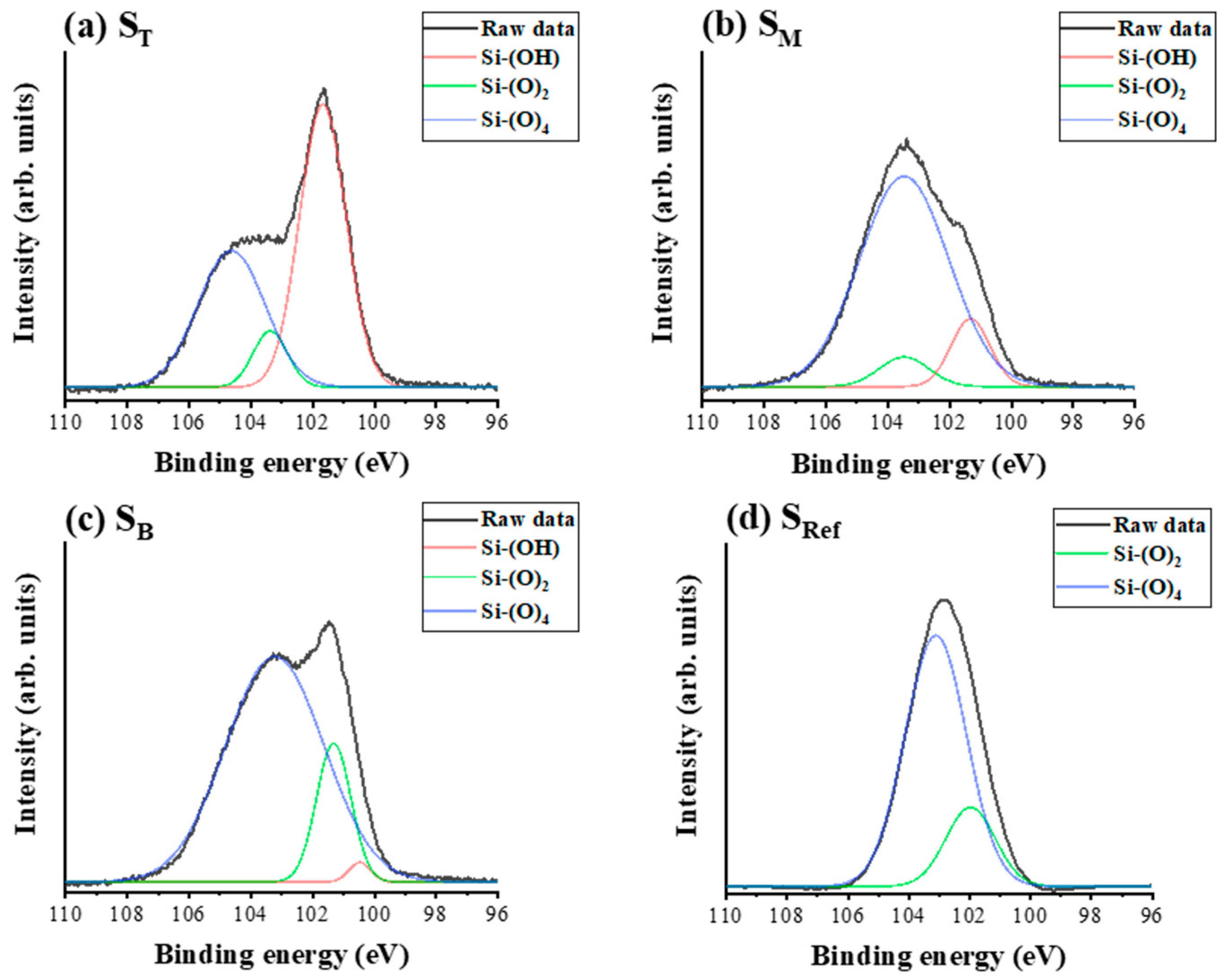
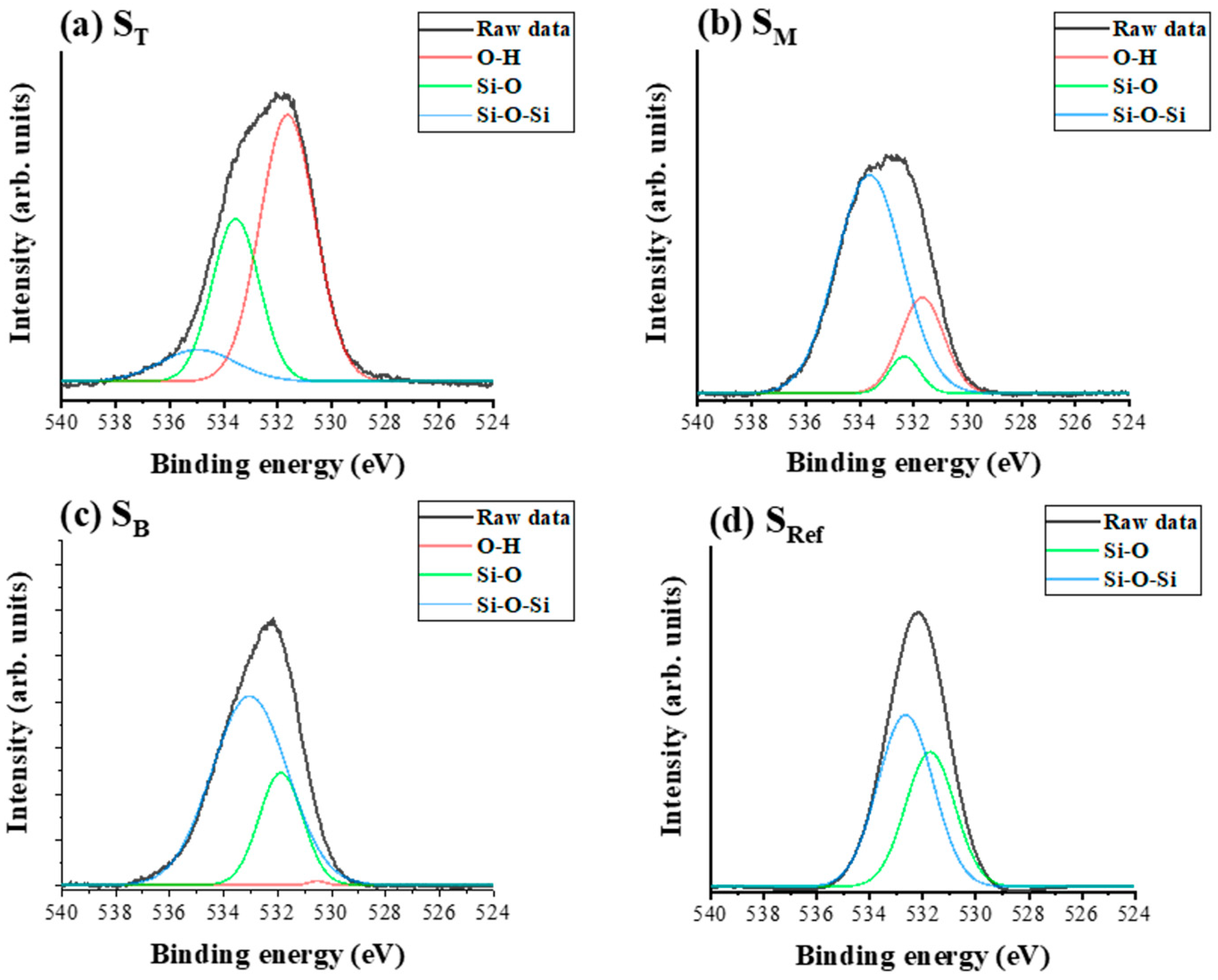
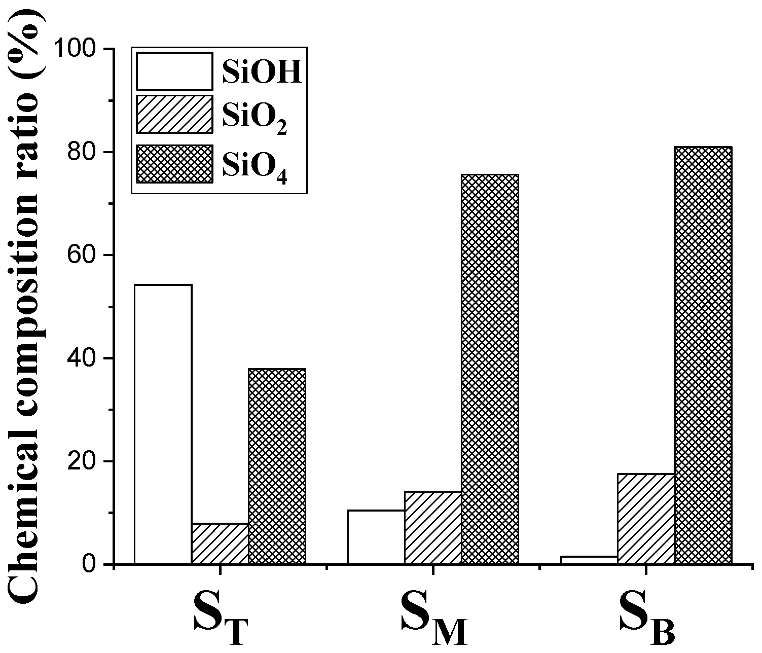
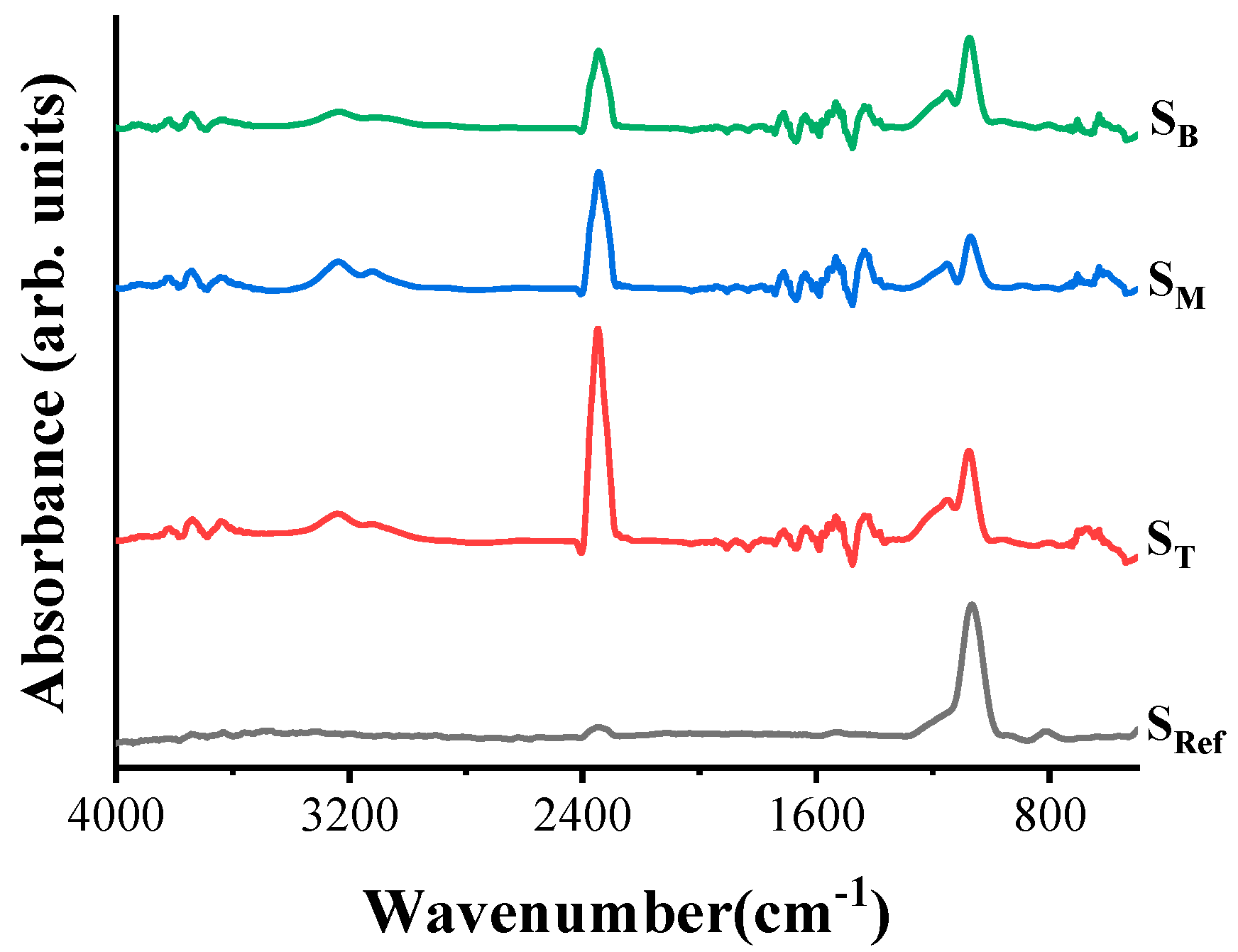
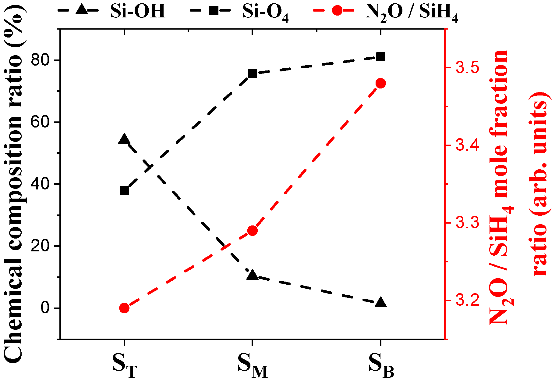
4.2. Chemical Composition and Bonding States

XPS wide scan spectra (Figure 6) showed dominant peaks corresponding to Si 2p (~102 eV), O 1s (~532 eV), and minor peaks for carbon, fluorine, and nitrogen, indicating oxygen- and silicon-rich films [26,27,28]. The presence of nitrogen is attributed to the N2O gas used during deposition. Residual fluorine species originating from prior NF3 plasma cleaning are known to persist on chamber surfaces, contributing to the observed fluorine signals. Carbon signals are interpreted as noise artifacts inherent to the XPS measurement.
High-resolution Si 2p spectra (Figure 7) revealed deconvoluted peaks for the SRef at 101.9 eV (Si–O2) and 103.3 eV (Si–O4) [29]. In contrast, wall samples exhibited additional peaks at 100.6 eV (Si–OH), 102.3 eV (Si-O2), and 103.9 eV (Si–O4) [30]. The presence of Si–OH indicates higher hydrogen incorporation in the wall-deposited films, especially in ST. The term ‘Si–O2’ denotes silicon atoms bonded to two oxygen atoms, corresponding to stoichiometric SiOx (x < 2) environments, while ‘Si–O4’ refers to fully coordinated silicon atoms bonded to four oxygen atoms, characteristic of stoichiometric SiO2 structures.
Similarly, the O 1s spectra (Figure 8) showed peaks at 531.2 eV (O–H), 532.3 eV (Si–O), and 533.6 eV (Si–O–Si) [31]. The proportion of O–H bonding was noticeably higher in ST and decreased toward SB. Figure 9 quantitatively compares bonding ratios, demonstrating that the Si–OH content was ~40% at ST, ~30% at SM, and ~20% at SB, whereas the Si–O4 content increased from top to bottom, suggesting a transition from porous to dense bonding structures.
These trends were supported by FT-IR spectra (Figure 10), where broad absorption bands between 3200 and 3500 cm−1, characteristic of O–H stretching vibrations, were prominent in ST and weak in SB. Additionally, the peak at 2330 cm−1, observed only in wall samples, suggests additional hydrogen-containing species not present in the reference film. To understand the effect of hydrogen incorporation on bonding structure, we analyzed the Si–O–Si stretching region in the FT-IR spectra (950–1250 cm−1) [32]. Deconvolution (Figure 11) revealed two distinct peaks centered at 1080 cm−1 (corresponding to ~144° bonding angle) and 1140 cm−1 (~150° bonding angle). The area ratio of the 150°/144° peaks (Figure 12) was highest at ST (~0.65) and decreased progressively toward SB (~0.35), indicating that wider bonding angles were more prevalent in top-wall contaminants. This trend correlates with hydrogen content, implying that hydrogen incorporation loosens the Si–O–Si network, resulting in wider bonding angles and possibly lower film density. The elevated hydrogen content is likely due to lower surface temperature and enhanced exposure to energetic hydrogen radicals near the plasma source.
As shown in Figure 13, the simulated mole fraction ratio of SiH4/N2O followed the trend ST > SM > SB, aligning with the observed hydrogen content and Si–OH bond proportion. The top wall region (ST) is thus identified as a hydrogen-rich zone, whereas the bottom region (SB) is oxygen-rich. This gradient in gas phase chemistry appears to drive spatial variation in film composition and structure. Interestingly, although the ST exhibited a higher surface temperature (~90 °C) compared to the middle and bottom regions (~40 °C), it still showed the highest hydrogen content and Si–OH bonding ratio. This suggests that factors such as higher SiH4 concentration and increased exposure to energetic plasma species at the top wall may have played a more dominant role than thermal desorption in determining hydrogen incorporation.

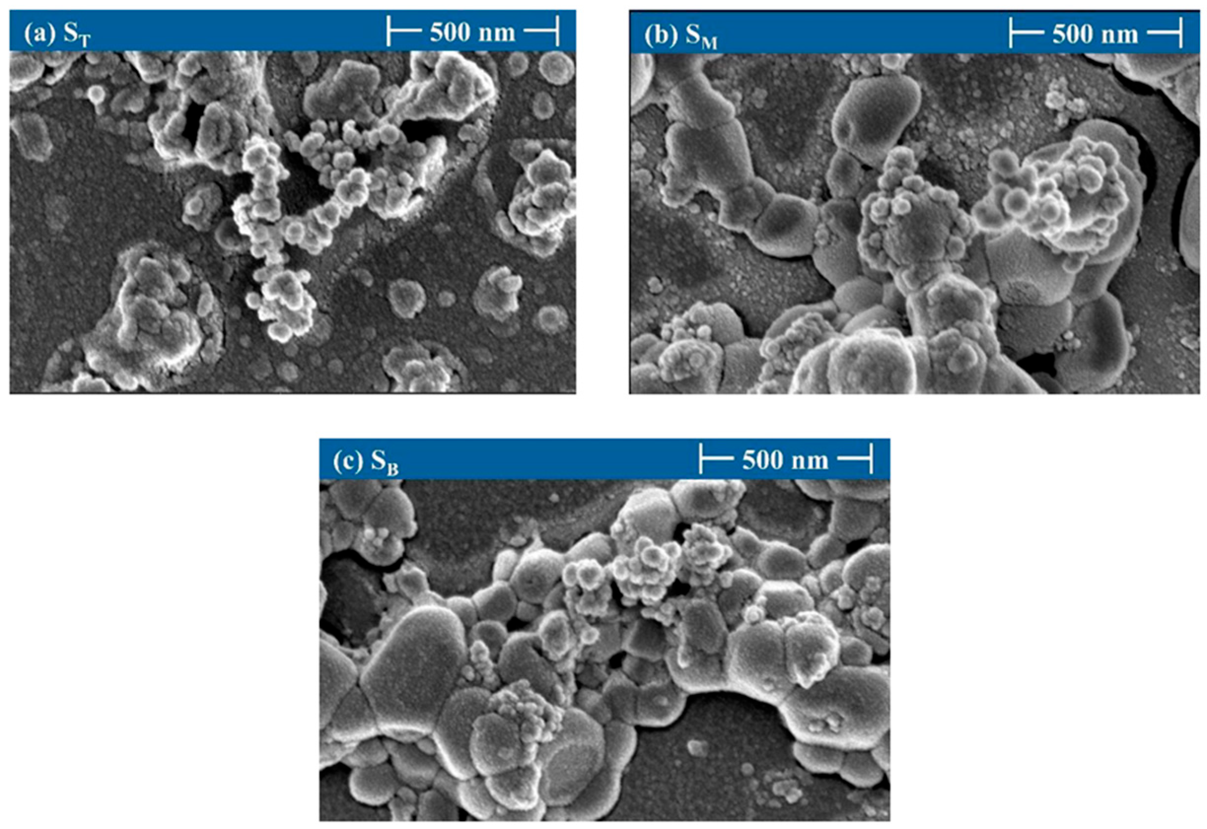
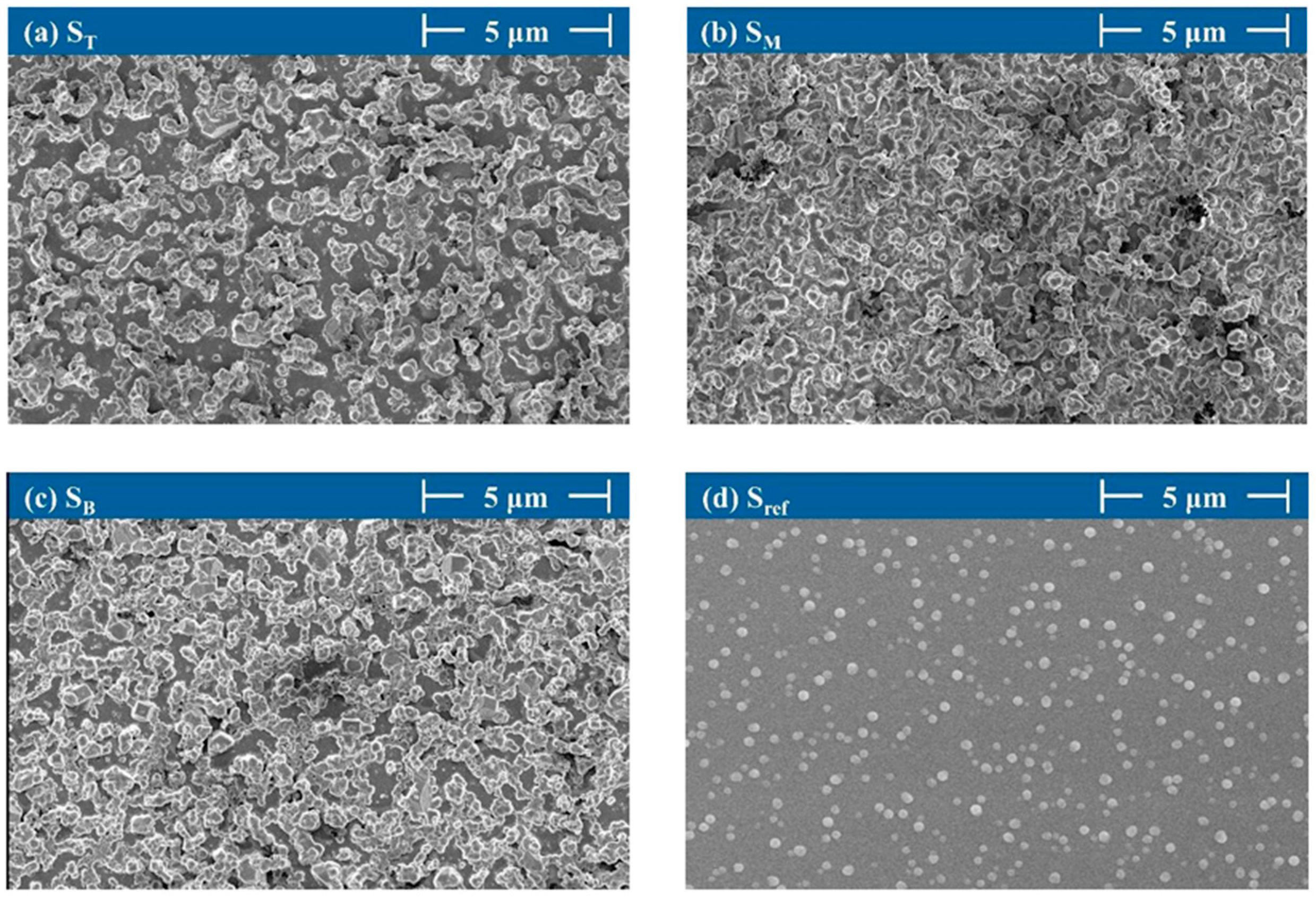
4.3. Surface Morphology and Particle Size

AFM surface images (Figure 14) revealed significant morphological differences between wall positions. The RMS roughness (Rq) increased from ~1.8 nm at ST, to ~2.4 nm at SM, and ~3.5 nm at SB, indicating more uneven and aggregated structures toward the bottom. SEM images (Figure 15 and Figure 16) confirmed these observations as ST showed fine, evenly distributed features, whereas SB exhibited large, irregular SiO particle clusters likely formed from fully reacted and cooled precursors. This suggests that particle aggregation and film roughness are more severe in the bottom region, making it more susceptible to flaking and particle shedding during subsequent processing.

4.4. Implications for ISD Process

The high hydrogen content and wide bonding angles in ST suggest that this region may be more reactive to fluorine-based ISD chemistry, enabling faster and more complete removal. In contrast, the SB region contains denser, larger particulates with lower hydrogen, potentially making it more resistant to ISD and a greater source of particle contamination if not fully removed. These findings imply that cleaning efficiency in ISD is strongly position-dependent, and adaptive chamber conditioning strategies may be required such as an elevated bottom wall temperature or differentiated coating thickness for top versus bottom regions. Our findings suggest that in situ dry-cleaning (ISD) processes could be optimized by targeting denser deposits at the bottom wall regions through longer cleaning durations or locally elevated temperatures. Furthermore, tailoring gas flow distribution during deposition or applying protective coatings selectively on the lower walls may enhance chamber maintenance efficiency and reduce particle-related defects. Understanding the vertical variation in wall film properties enables a more precise design of ISD protocols, ultimately improving chamber stability, reducing maintenance frequency, and enhancing process yield in semiconductor manufacturing.

5. Conclusions

This study investigated the spatial variation in chemical composition and surface morphology of contaminant films deposited on the inner walls of a PECVD chamber during SiO2 film deposition. By attaching long silicon coupons to the chamber side walls and analyzing the resulting films using XPS, FT-IR, AFM, and SEM, we identified significant differences in film characteristics based on vertical position. The contaminants formed on the ST exhibited higher hydrogen content, greater Si–OH bond concentration, and wider Si–O–Si bonding angles compared to the middle (SM) and bottom (SB) regions. These trends are attributed to the higher SiH4/N2O ratio and closer proximity to the plasma, resulting in more active hydrogen reactions. In contrast, the bottom wall showed lower hydrogen content, denser bonding structures, larger particulate agglomerates, and greater surface roughness. These spatial variations are strongly influenced by gas flow dynamics, precursor residence time, and plasma energy distribution within the chamber. Although temperature differences were observed across wall positions, the spatial variation in contamination composition appears to be more closely linked to plasma exposure and precursor distribution rather than temperature alone. From a practical standpoint, these findings imply that the top wall region may be cleaned more efficiently during ISD due to its porous, hydrogen-rich structure. However, the bottom wall, with its dense, rigid contaminants, may pose a challenge for cleaning and could serve as a persistent particle source if not properly managed. Therefore, localized strategies such as increasing the bottom-wall temperature or applying thicker protective coatings at specific regions are recommended to enhance cleaning uniformity and chamber stability. This work provides a foundation for improved chamber conditioning and cleaning process optimization in PECVD systems, with implications for enhancing process reproducibility and minimizing particle-induced yield loss in semiconductor manufacturing.

Author Contributions

Conceptualization, S.J.H.; methodology, S.J.H. and J.L.; software, J.J.; validation, S.J.H.; formal analysis, J.L. and S.J.H.; investigation, J.L.; data curation, J.L.; writing—original draft preparation, J.L. and J.J.; writing—review and editing, S.J.H.; visualization, J.L. and J.J.; supervision, S.J.H.; project administration, S.J.H.; funding acquisition, S.J.H. All authors have read and agreed to the published version of the manuscript.

Funding

This research was supported by a National Research Council of Science & Technology (NST) grant by the Korea government (MSIT) (CRC20014-000).

Institutional Review Board Statement

Not applicable.

Informed Consent Statement

Not applicable.

Data Availability Statement

The data presented in this study are available on request from the corresponding author due to the restrictions from the associated semiconductor equipment industry.

Acknowledgments

The authors are grateful to DISCO Hi-TEC Korea Corporation for the 300 mm wafer dicing support.

Conflicts of Interest

The authors declare no conflicts of interest. The funders had no role in the writing of the manuscript.

References

  1. Kim, M.; Kwon, H.; Kim, H.; Park, S.; Lee, J.; Na, K.; Kong, C.; Kim, Y. First Wafer Effect of Multiple SiO2/SiN Stack Layers Prepared by using Plasma-enhanced Chemical Vapor Deposition. J. Korean Phys. Soc. 2020, 76, 911. [Google Scholar] [CrossRef]
  2. Heydari Gharahcheshmeh, M. Fabrication of Conjugated Conducting Polymers by Chemical Vapor Deposition (CVD) Method. Nanomaterials 2025, 15, 452. [Google Scholar] [CrossRef] [PubMed]
  3. Faggio, G.; Politano, G.G.; Lisi, N.; Capasso, A.; Messina, G. The structure of chemical vapor deposited graphene substrates for graphene-enhanced Raman spectroscopy. J. Phys. Condens. Matter 2024, 36, 195303. [Google Scholar] [CrossRef] [PubMed]
  4. Raoux, S.; Liu, K.S.; Guo, X.; Silvetti, D. In-situ RF diagnostic for PECVD process control. MRS Online Proc. Libr. 1997, 502, 53. [Google Scholar] [CrossRef]
  5. Young, B.; Yoo, K.; Chung, C. Real-time observation of the capacitance variation in a surface dielectric layer in radio frequency discharge. J. Appl. Phys. 2012, 111, 036805. [Google Scholar] [CrossRef]
  6. Jellum, G.M.; Graves, D.B. Particle-plasma interactions in low-pressure discharges. Appl. Phys. Lett. 1990, 57, 2077. [Google Scholar] [CrossRef]
  7. Kim, J.; Chung, C. Real-time dielectric-film thickness measurement system for plasma processing chamber wall monitoring. Rev. Sci. Instrum. 2015, 86, 123677. [Google Scholar] [CrossRef]
  8. Masuda, A.; Ishibashi, Y.; Uchida, K.; Kamesaki, K.; Izumi, A.; Matsumura, H. In situ chamber cleaning using atomic H in catalytic-CVD apparatus for mass production of a-Si: H solar cells. Sol. Energy Mater. Sol. Cells 2002, 74, 373–381. [Google Scholar] [CrossRef]
  9. Xu, S.; Sun, Z.; Qian, X.; Holland, J.; Podlesnik, D. Characteristics and mechanism of etch process sensitivity to chamber surface condition. J. Vac. Sci. Technol. B 2001, 19, 166–171. [Google Scholar] [CrossRef]
  10. Park, H.K.; Song, W.S.; Hong, S.J. In situ plasma impedance monitoring of the oxide layer PECVD process. Coatings 2023, 13, 559. [Google Scholar] [CrossRef]
  11. Cunge, G.; Pelissier, B.; Joubert, O.; Ramos, R.; Maurice, C. New chamber walls conditioning and cleaning strategies to improve the stability of plasma processes. Plasma Sources Sci. Technol. 2005, 14, 599–606. [Google Scholar] [CrossRef]
  12. Boudaden, J.; Altmannshofer, S.; Wieland, R.; Pittroff, M.; Eisele, I. An Approach to Reduce Greenhouse Gases in the Semiconductor Industry Using F2 Dissociated in Plasma for CVD Chamber Cleaning. Appl. Sci. 2018, 8, 846. [Google Scholar] [CrossRef]
  13. Rößler, T.; Albert, M.; Terasa, R.; Bartha, J.W. Alternative etching gases to SF6 for plasma enhanced chamber cleaning in silicon deposition systems. Surf. Coat. Technol. 2005, 200, 552–556. [Google Scholar] [CrossRef]
  14. An, S.; Hong, S.J. Spectroscopic analysis of NF3 plasmas with oxygen additive for PECVD chamber cleaning. Coatings 2023, 13, 91. [Google Scholar] [CrossRef]
  15. Jang, H.; Lee, J.; Kim, Y.; Lee, S.; Hong, S.J. Real-time endpoint detection of small exposed area SiO2 films in plasma etching using plasma impedance monitoring with modified principal component analysis. Plasma Process. Polym. 2013, 10, 850–856. [Google Scholar] [CrossRef]
  16. Lee, H.; Seo, D.; Hong, S.; May, G. PECVD Chamber cleaning end point detection (EPD) using optical emission spectroscopy data. Trans. Electr. Electron. Mater. 2013, 14, 254–258. [Google Scholar] [CrossRef]
  17. Lucken, R.; Croes, V.; Lafleur, T.; Raimbault, J.L.; Bourdon, A.; Chabert, P. Edge-to-center plasma density ratios in two-dimensional plasma discharges. Plasma Sources Sci. Technol. 2018, 27, 035004. [Google Scholar] [CrossRef]
  18. You, Y.M.; Lee, J.S.; Kim, M.H.; Hong, S.J. Use of plasma process diagnostic sensors for the monitoring of in situ dry cleaning of plasma enhanced chemical vapor deposition chamber. J. Vac. Sci. Technol. B. 2024, 42, 042203. [Google Scholar] [CrossRef]
  19. Le Gouil, A.; Pargon, E.; Cunge, G.; Joubert, O.; Pelissier, B. Chemical analysis of deposits formed on the reactor walls during silicon and metal gate etching processes. J. Vac. Sci. Technol. B 2006, 24, 2191–2197. [Google Scholar] [CrossRef]
  20. Xu, X.; Feng, J.; Liu, X.M.; Wang, Y.N.; Yan, J. Study of the neutral gas flow on discharges of capacitively coupled plasma in a PECVD reactor. Vacuum 2013, 92, 1–6. [Google Scholar] [CrossRef]
  21. Gusev, E.Y.; Jityaeva, J.Y.; Ageev, O.A. Effect of PECVD conditions on mechanical stress of silicon films. Mater. Phys. Mech. 2018, 37, 67–73. [Google Scholar] [CrossRef]
  22. Pan, P.; Nesbit, L.A.; Douse, R.W.; Gleason, R.T. The Composition and Properties of PECVD Silicon Oxide Films. J. Electrochem. Soc. 1985, 132, 2012. [Google Scholar] [CrossRef]
  23. Overzet, L.J.; Verdeyen, J.T. Enhancement of the plasma density and deposition rate in rf discharges. Appl. Phys. Lett. 1986, 48, 695–697. [Google Scholar] [CrossRef]
  24. Greczynski, G.; Hultman, L. X-ray photoelectron spectroscopy: Towards reliable binding energy referencing. Prog. Mater. Sci. 2020, 107, 100591. [Google Scholar] [CrossRef]
  25. Pan, Y.; Liu, H.; Wang, Z.; Jia, J.; Zhao, J. Optical constant and conformality analysis of SiO2 thin films deposited on linear array microstructure substrate by PECVD. Coatings 2021, 11, 510. [Google Scholar] [CrossRef]
  26. Jeong, H.; Cho, J. Fabrication and evaluation of protective SiOx layers using plasma-enhanced chemical vapor deposition. Surf. Coat. Technol. 2017, 330, 71–78. [Google Scholar] [CrossRef]
  27. Alam, A.U.; Howlader, M.M.R.; Deen, M.J. Oxygen Plasma and Humidity Dependent Surface Analysis of Silicon, Silicon Dioxide and Glass for Direct Wafer Bonding. ECS J. Solid State Sci. Technol. 2013, 2, P515–P523. [Google Scholar] [CrossRef]
  28. Alexander, M.R.; Short, R.D.; Jones, F.R.; Michaeli, W.; Blomfield, C.J. A study of HMDSO/O2 plasma deposits using a high-sensitivity and -energy resolution XPS instrument: Curve fitting of the Si 2p core level. Appl. Surf. Sci. 1999, 137, 179–185. [Google Scholar] [CrossRef]
  29. Ma, H.; Yang, J.; Yang, J.; Zhu, L.; Huang, W.; Yuan, G.; Feng, J.; Jen, T.; Lu, H. Systematic Study of the SiOx Film with Different Stoichiometry by Plasma-Enhanced Atomic Layer Deposition and Its Application in SiOx/SiO2 Super-Lattice. Nanomaterials 2019, 9, 55. [Google Scholar] [CrossRef]
  30. Zhang, Y.; Zhu, L.; Chen, L.; Liu, L.; Ye, G. Influence of Magnesia on Demoulding Strength of Colloidal Silica-Bonded Castables. Rev. Adv. Mater. Sci. 2019, 58, 32–38. [Google Scholar] [CrossRef]
  31. Deshmukh, S.C.; Aydil, E.S. Investigation of low temperature SiO2 plasma enhanced chemical vapor deposition. J. Vac. Sci. Technol. B 1996, 14, 738–745. [Google Scholar] [CrossRef]
  32. Peng, Z.W.; Hsieh, P.T.; Lin, Y.J.; Huang, C.J.; Li, C.C. Investigation on Blistering Behavior for n-type Silicon Solar Cells. Energy Procedia 2015, 77, 827–832. [Google Scholar] [CrossRef]
Figure 1. Modeling of the PECVD chamber: (a) front view and (b) isometric view.
Coatings 15 00563 g001
Figure 2. Structure of the showerhead: (a) front view and (b) top view.
Coatings 15 00563 g002
Figure 3. Top view of the PECVD chamber mesh.
Coatings 15 00563 g003
Figure 4. Experimental schematic for the acquisition of contaminants in the chamber wall.
Coatings 15 00563 g004
Figure 5. Comparison of thickness of wall samples and gas average velocity according to wall positions.
Coatings 15 00563 g005
Figure 6. XPS wide scan spectra according to sample positions.
Coatings 15 00563 g006
Figure 7. Deconvolved peaks of Si 2p XPS narrow scan spectra based on sample positions: (a) ST, (b) SM, (c) SB, and (d) SRef.
Coatings 15 00563 g007
Figure 8. Deconvolved peaks of O 1s XPS narrow scan spectra based on sample positions: (a) ST, (b) SM, (c) SB, and (d) SRef.
Coatings 15 00563 g008
Figure 9. Chemical composition ratio according to wall positions.
Coatings 15 00563 g009
Figure 10. FTIR full spectra according to sample positions.
Coatings 15 00563 g010
Figure 11. Deconvolved spectra of the Si–O–Si stretching mode region according to sample positions.
Coatings 15 00563 g011
Figure 12. Comparison of bonding angle ratio (144°/150° Si–O–Si bonding angle) according to sample positions.
Coatings 15 00563 g012
Figure 13. Comparison of variation in N2O/SiH4 mole fraction and composition of wall sample according to wall positions.
Coatings 15 00563 g013
Figure 14. Three-dimensional surface images according to wall positions: (a) ST, (b) SM, and (c) SB.
Coatings 15 00563 g014
Figure 15. SEM images according to wall positions: (a) ST, (b) SM, and (c) SB.
Coatings 15 00563 g015
Figure 16. Low-magnification SEM images according to wall positions: (a) ST, (b) SM, (c) SB and (d) Sref.
Coatings 15 00563 g016
Table 1. Boundary conditions.
Boundary Conditions
Pressure (mTorr)500
Chuck temperature (°C)300
Mass flow rate
[sccm]
SiH49
N2O35
Ar2
Table 2. Experimental recipe for the acquisition of contaminants in the chamber wall.
Power (W)Pressure
(mTorr)
Gas Flow Rate (sccm)Temp (°C)
SiH4N2OAr
3505009352300
Disclaimer/Publisher’s Note: The statements, opinions and data contained in all publications are solely those of the individual author(s) and contributor(s) and not of MDPI and/or the editor(s). MDPI and/or the editor(s) disclaim responsibility for any injury to people or property resulting from any ideas, methods, instructions or products referred to in the content.

