Article

In Situ Plasma Impedance Monitoring of the Oxide Layer PECVD Process

Department of Electronics Engineering, Myongji University, Yongin 17058, Republic of Korea
*
Author to whom correspondence should be addressed.
Coatings 2023, 13(3), 559; https://doi.org/10.3390/coatings13030559
Submission received: 24 January 2023 / Revised: 27 February 2023 / Accepted: 2 March 2023 / Published: 5 March 2023
(This article belongs to the Special Issue Recent Advances in Semiconducting Thin Films)

Abstract

:
The use of plasma in semiconductor fabrication processes has been continuously increasing because of the miniaturization of semiconductor device structure, and plasma enhanced chemical vapor deposition (PECVD) has become a major process in thin film deposition. As a consequence, plasma diagnosis has become crucial during the deposition process, but the lack of in situ plasma monitoring sensors requires further development of existing in situ sensors, such as the Langmuir probe and optical emission spectroscopy (OES), for in situ plasma process monitoring. In this study, electrically equivalent circuit models of the PECVD chamber functioned as a plasma impedance model with respect to the deposited thin film thickness while plasma impedance was measured using a radio frequency voltage–current (VI) probe. We observed a significant correlation between the deposited film thickness of the chamber wall and the measured impedance of the PECVD chamber cleaning application in the semiconductor industry.

Graphical Abstract

1. Introduction

Recently, the use of plasma equipment has increased due to the miniaturization of semiconductor devices, such as NAND flash; particularly, the development of plasma deposition equipment has increased, and plasma diagnosis has become necessary in the deposition of oxide or nitride films [1]. Additionally, in this process, the control of factors such as film deposition thickness and uniformity are important [2]. Therefore, many sensors to diagnose plasma have been studied.
Sensors for diagnosing plasma are primarily divided into electrical and optical sensors. Electrical diagnostic sensors mainly include the single Langmuir probe (SLP) [3,4], voltage–current (VI) probe [5,6], cut-off probe [7,8], floating probe [9,10], curling probe [11,12], and hairpin probe [13,14]. In addition, optical diagnostic sensors include optical emission spectroscopy (OES) [15,16,17,18,19].
The SLP is an intuitive sensor that can directly measure the plasma parameters of electron density (ne) and electron temperature (Te). Plasma potential (Vp) and the electron energy distribution function (EEDF) can be simply calculated using plasma parameters. However, it is unfortunate that inserting any undesired object into the plasma chamber (other than the wafer) during the process is not permitted in the semiconductor manufacturing environment due to plasma perturbation. The Langmuir probe, crucially, suffers from material deposition on the probe tip-end [20,21,22].
OES is a well-known non-invasive in situ plasma monitoring sensor, primarily used as an end point detector [23,24,25]. The benefits of OES are its non-invasiveness to the plasma during the process and convenient installation; however, its analysis can be complex. It also suffers from data drift over time due to viewport contamination [26,27,28]. Recently, numerous efforts have been made to find plasma parameters based on the phenomenological approach; however, the process of defining the collisional radiative model for mixed gas in a higher pressure region (>1 Torr) is complicated when a collision needs to be considered. It is also more complicated for molecular gases such as N2 than it is for rare gases such as Ar, for which many cases of dielectric deposition involve plasma-enhanced chemical vapor deposition (PECVD). Plasma parameters are generally calculated through the vibration level of N2 [29]. However, this may be more inaccurate than probe measurements because it only considers some chemical reactions in the plasma. Electrical sensors have also been investigated regarding plasma monitoring and analysis to alleviate concerns. However, the insertion type of electrical sensor is vulnerable to erosion/deposition of its electrical sensor. Some efforts to alleviate these concerns have also been investigated [30]. However, they are still invasive and change the properties of the plasma. Given this, much-used plasma diagnostic tools cannot be applied to the plasma deposition process due to deposition of the measurement site.
Plasma is diagnosed using a VI probe, a type of electrical sensor, to solve the problem of plasma characteristics change. Plasma impedance monitoring using a VI probe is another non-invasive monitoring sensor for the plasma process/equipment diagnosis. Unlike OES, a VI probe is an electrical diagnostic sensor that measures voltage and current to calculate their phases from the plasma equipment’s radio frequency (RF) network. Plasma generated by the applied RF power can be electrically modeled using an equivalent circuit model [31,32,33,34,35]. Still, the impedance of plasma should be tightly controlled by the automated impedance matching unit, known as the RF impedance matcher. Impedance matching determines the amount of reflected power, which affects the deposited film thickness and thin film quality of PECVD [36]. During PECVD, one of the key process quality measurements is the deposited film’s thickness. A previous study revealed the relationship between plasma reactance and deposition thickness employing a VI probe.
Motivated by the effect of plasma impedance change on the deposited thin film’s thickness, we extended the use of the VI probe to investigate the deposited film’s thickness on a wafer, the showerhead and the chamber wall. We initially performed 30 consecutive runs to understand the plasma reactance variability using a simple equivalent circuit model as a preliminary study. As shown in Figure 1, the simple conversion of plasma reactance holds excellent variability. The apparent results cannot be accepted as an in situ deposition monitoring of the thin film’s thickness. To investigate the relationship between the deposited film’s thickness and plasma reactance, the plasma sheath model and plasma equivalent circuit model were considered with respect to the RF matching network of the PECVD equipment. Established hypotheses were verified using a silicon dioxide (SiO2) deposition experiment on 6-inch wafers; we found that plasma reactance is proportional to the deposited film’s thickness.
Section 2 presents the Child–Langmuir law and an interpretation model for non-invasive plasma diagnosis. Section 3 describes the experimental conditions and equipment. Section 4 describes the deposition thickness and impedance measured through oxide deposition experiments using 6-inch PECVD equipment, followed by the conclusion in Section 5.

2. Method

2.1. Child–Langmuir Law

In general, the sheath thickness is thicker than the film thickness, so the sheath thickness has a significant effect on reactance measurement. Therefore, it is necessary to define the sheath for deposited film thickness calculations. Hence, this study assumed the Child–Langmuir sheath. Plasmas are also generally classified as collision-less at low pressures and collisional at high pressures. The collision model of plasma is used above the intermediate pressure region. Therefore, it is necessary to modify the sheath model [37,38] to define the sheath thickness. Generally, the sheath thickness is used as the collision-less Child–Langmuir law [39]. For these reasons, a modified Child–Langmuir sheath was applied to the collisional sheath. This collision-less Child–Langmuir model is divided into constants of ion mobility and ion mean free path.
Collision-less Child–Langmuir law:
s m = 2 3 ( ε 0 ) 1 / 2 ( 2 e m ) 1 / 4 V ¯ sh 3 / 4 J ¯ i 1 / 2
Therefore, the collisional sheath thickness can be expressed as in [34] (p. 147).
  • Voltage drive
Collisional Child–Langmuir law (constant ion mean free path):
s m = 1.68 2 / 5 ( ε 0 ) 2 / 5 ( 2 e λ i m ) 1 / 5 V ¯ sh 3 / 5 J ¯ i 2 / 5
Collisional Child–Langmuir law (constant ion mobility):
s m = ( 9 8 ) 1 / 3 ( ε 0 μ i ) 1 / 3 V ¯ sh 2 / 3 J ¯ i 1 / 3
V ¯ sh = ( K s K cap ) s m I 0 ω ε 0 A
J ¯ i = e h l n 0 u B
Here, s m is the sheath thickness, ε 0 is the permittivity of vacuum, m is the ion mass, e is the electric charge, J ¯ i is the average ion current density, V ¯ sh is the average sheath voltage, μ i is the mobility of ions, I 0 is the current amplitude, A is the area, K s and K cap are constants, h l is the edge–center density ratio, n 0 is the plasma bulk density, and u B is the Bohm velocity. However, as in this study, the average sheath voltage and average ion current density cannot be measured directly using the VI probe. Therefore, the current drive is converted to the current density as follows.
  • Current drive
Substituting Equations (4) and (5) into voltage drive Equations (2) and (3),
Collisional Child–Langmuir law (constant ion mean free path):
s m = 0.88 ( λ i ε 0 k T e ω 3 e h l 2 A 3 ) 1 / 2 I 0 3 / 2 n 0
Collisional Child–Langmuir law (constant ion mobility):
s m = 0.423 μ i 1 e h l n 0 u B ε 0 ( I 0 ω A ) 2
Here, λ i is the ionic mean free path, T e is the electron temperature, and k is the Boltzmann constant.

2.2. Plasma Equivalent Circuit

Next, we define the plasma using the plasma equivalent circuit model required for diagnosis using the VI probe. Plasma equivalent circuits have been studied under various conditions [34,35] (p. 142, p. 399). Therefore, a suitable equivalent circuit is considered for intermediate pressure as 1 Torr. In Figure 2, the plasma equivalent circuit can be divided mainly into sheath and bulk. Additionally, the deposition capacitance is related to the deposited film’s thickness. Each element is as follows.
R ohm = 1.14 s m λ i h l m ν m l 2 s m ω e I 0 3 / 2 A ε 0 s m k T e 1 / 2
L p = ν m R ohm
R stoc = 0.8 m k T e 1 / 2 ω s m e I 0
R i = 0.9 s m λ i e s m I 0 m ε 0 3 A 3 ω 5
R ohm , sh = 0.155 m ν m s m ω s m e I 0
C s = 0.751 ε 0 A s m
where s m is sheath thickness, λ i is ion mean free path, h l is bulk-sheath edge density ratio, m is ion mass, ν m is electron-neutral collision frequency, ω is RF angular frequency, I 0 is current amplitude, A is the area (electrode), ε 0 is the permittivity of vacuum, k is the Boltzmann constant, T e is the electron temperature, and l is the bulk length.
The meaning of Equations (8)–(13) can be explained as follows. Equation (8) R ohm is the ohmic heating resistance (heating due to electron and neutron collisions). Equation (9) L p is the plasma inductance (electron inertia). Equation (10) R stoc is the stochastic heating resistance (electron and electric field repulsion). Equation (11) R i is the ion resistance (power loss due to ions being accelerated in each sheath). Equation (12) R ohm , sh is the sheath ohmic resistance, and Equation (13) C s is the sheath capacitance. At high pressure, the sheath thickness decreases, and the bulk length becomes relatively long [40]. Therefore, the plasma capacitance C 0 = ε 0 l A considered in the reference can be neglected.

3. Experimental Apparatus

As shown in Figure 3, the experiment was conducted in 6-inch capacitively coupled plasma (CCP-type) PECVD equipment, a mini-plasma station manufactured by Plasmart, Daejeon, Republic of Korea. A matcher from a 13.56 MHz RF generator supplied power to the chamber. In addition, Z-scan, manufactured by Advanced Energy Industries, Denver, CO, USA, was installed between the matcher and the electrode. Z-scan measured voltage, current, and phase differences. Therefore, resistance and reactance could be calculated. The sensor stored law data every 0.103 s (the device’s specification). Due to the impedance matching problem, the plasma did not stabilize for approximately 30 s; therefore data after 30 s was used. In addition, the chuck and wafer were heated to 200 °C through the heater located on the lower chuck for the dielectric deposition.
The experiment was designed around the phenomenon of changing deposition thickness ( d dep ) with time, as shown in Figure 3a,b, which affects capacitance ( C dep ). The material being deposited, in particular, focuses on SiO2. In Figure 3a, C dep was divided into two factors, C dep , wall (deposition capacitance of the wall and showerhead) and C dep , wafer (deposition capacitance on the wafer), which is discussed in more detail later.
The SiO2 film was deposited using SiH4 and N2O for oxide film deposition. In addition, chamber cleaning was performed by injecting NF3 and a small amount of Ar. The standard recipe is shown in Table 1. In addition, the cleaning recipe shown in Table 1 was used to remove deposits or particles on the walls. The experiment was conducted to minimize sheath thickness variation by increasing the deposition time using the same recipe.
As shown in Table 2, each experiment that used the above recipe (Table 1) was classified as Experiment 1 and Experiment 2. In Experiment 1, deposition was performed while increasing the time by 150 s from 150 to 900 s. In addition, in Experiment 2, 150 s reproducibility experiments were performed from No. 1 to 6. In each case, a separate experiment was conducted with one cleaning and without (w/o) cleaning.
In addition, the wafer was replaced after opening the chamber between each process. After the deposition, the thin film’s thickness was measured using a reflectometer, ST 2000, manufactured by NRP, Daejeon, Republic of Korea.

4. Results and Discussion

4.1. Assumptions

In this study, the following were assumed to monitor the impedance of the deposition thickness.
  • We used the Child–Langmuir law (intermediate pressure), where λ i << λ De .
  • As only fluctuations due to deposition were considered, the impedance of the chamber itself was not considered.
  • There was no change in plasma parameters during the process. Hence, there was no change in sheath thickness.

4.2. Analysis Model

The model in Figure 2 was modified to diagnose film thickness change using VI probe measurements.
R total + j ω X total = R ohm + 2 R ohm , sh + 2 R i + j ω X s + X p + X dep
Here, R total is total resistance, X total is total reactance (measured using Z-scan), X s is sheath resistance (associate sheath thickness), X p is plasma bulk reactance, and X dep is deposition reactance. As shown in Figure 4, the reactance can be considered a series connection of parallel bulk capacitance, sheath capacitance, and deposition capacitance. In this case, the bulk length was greater than the sheath thickness. Therefore, bulk capacitance was neglected as it had a negligible effect on reactance. In addition, the reactance of the plasma was capacitive. Thus, the influence of the two factors, X s and X dep , was large. However, the sheath thickness (approximately 10−2 m) was thicker than the deposition thickness (approximately 10−10 m). Therefore, the effect of the sheath thickness on the reactance was dominant. The sheath thickness could not be measured non-invasively within the scope of this study. Consequently, it was necessary to assume that there was no change in sheath thickness.

4.3. Constant Sheath Thickness

Previously, a constant sheath thickness was assumed to minimize the effect of the sheath thickness. However, the actual impact on reactance was large. Therefore, the sheath thickness is
s m = 0.88 λ i ε 0 k T e ω 3 e h l 2 A 3 1 / 2 I 0 3 / 2 n 0
R ohm = 1.14 s m λ i h l m ν m l 2 s m ω e I 0 1 / 2 A ε 0 s m k T e 1 / 2
Summarizing Equations (15) and (16) for the sheath thickness,
s m λ i 1 / 2 I 0 3 / 2
s m R ohm λ i 1 / 2 I 0 3 / 2
Δ   s m R ohm I 0 3 / 2
Equations (17) and (18) show that the sheath thickness is composed of current and resistance. Additionally, λ i is proportional to p 1 2 . However, as there was no recipe change (power, pressure, and gas flow), we assumed that there was no change. So, Δ s m is expressed by Equation (19). As shown in Figure 5, it can be confirmed that the sheath thickness was constant during the process.

4.4. Reactance Reproducibility Problem

Figure 6 analyzes the problem of reactance reproducibility when measured using the VI probe. In the case of one cleaning, a reactance change of approximately Δ 0.5 Ω occurred. However, a considerable change of approximately Δ 1.5–3.5 Ω occurred when cleaning was not performed. These changes in the reactance were due to moisture absorption by the oxide film when the chamber was opened [41] and oxide deposition on the wall or inside the chamber [15,26].

4.5. Change in Reactance (Considering Only the Deposition on the Wafer)

The total reactance in the equivalent circuit in Figure 4 can be expressed as Equation (20).
j ω X total = j ω X s + X p + X dep
Components of the reactance consist of sheath reactance, plasma reactance (inductance), and deposition reactance. As the sheath thickness was said to be constant, the sheath reactance could be ignored. The inductance component was also ignored, as the reactance had a negative value in the experiment. Therefore, the total reactance was determined by the deposition reactance.
j ω X total = j ω d dep ω 2 ε 0 A
X total d dep
Δ   X total Δ   d dep
As shown in Equations (21)–(23), the deposition thickness is proportional to the total reactance. However, as shown in Figure 6b, it was confirmed that the reactance decreases exponentially over time. Therefore, the deposition thickness should increase exponentially. To confirm this, results were compared with the thin film’s thickness measured using a reflectometer. d dep is the deposition thickness on the wafer ( C d e p = ε 0 d d e p A ).
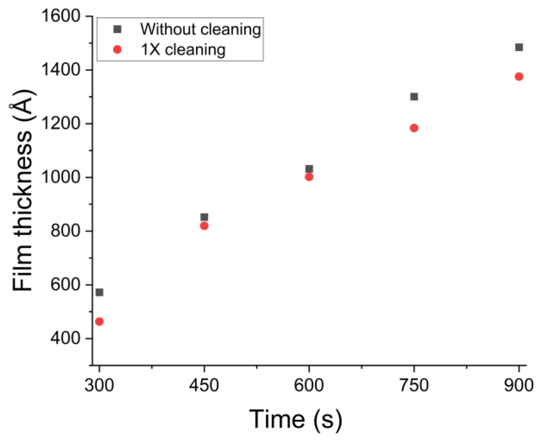
As shown in Figure 7, it was confirmed that the deposited film’s thickness was close to linear rather than an exponential increase with time. Therefore, a model with additional sources causing reactance change within the chamber with time is required.
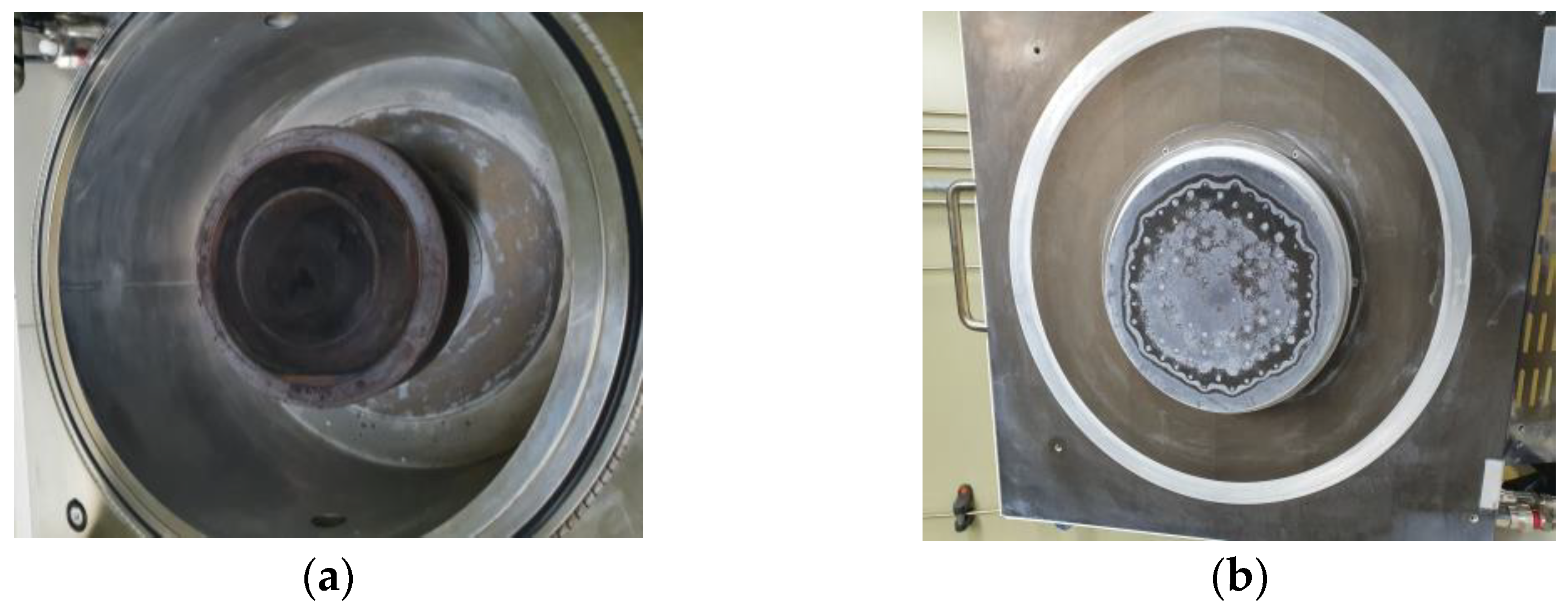
Figure 8 show that deposits were not deposited only on the wafer. Therefore, the formula was modified and analyzed based on the deposition on the chamber wall and the showerhead, and the above equivalent circuit was modified.

4.6. Change in Reactance (Considering Wall and Showerhead Deposition)

Based on the preceding phenomena, deposition on walls or the showerhead should be considered. Therefore, the above equivalent circuit was modified. As shown in Figure 9, C dep , wall was added in parallel to C dep to account for the deposition of the wall and the showerhead.
C dep = ε 0 A dep , wall d dep , wafer + A dep , wafer d dep , wall d dep , wall d dep , wafer
A dep , wall is the deposition area on the wall, A dep , wafer is the deposition area on the wafer, d dep , wall is the deposition thickness on the wall, and d dep , wafer is the deposition thickness on the wafer. C dep can be obtained by calculating the parallel capacitance as follows.
j ω X total = j ω d dep , wafer d dep , wall ω 2 ε 0 A dep , wall d dep , wafer
Substituting Equation (24) into the total reactance can be expressed as Equation (25). Additionally, usually A dep , wall > A dep , wafer , and d dep , wafer >> d dep , wall . Therefore, if we ignore the terms of d dep , wafer ,
j ω X total = j ω d dep , wall ω 2 ε 0 A dep , wall
Δ   j ω X total = Δ   j ω d dep , wall
As ω , ε 0 , and A dep , wall remain unchanged, Equation (26) is changed to Equation (27), as follows; the total reactance is composed of elements related to the wall and the showerhead.
But if A dep , wall > A dep , wafer , d dep , wafer (> or ≈) d dep , wall , so
C dep = ε 0 A dep ,   wall d dep , wafer + A dep , wafer d dep , wall d dep , wall d dep , wafer
It is expressed as in Equation (28). Also, if expressed as total reactance,
j ω X total = j ω d dep , wall d dep , wafer ω 2 ε 0 A dep , wall d dep , wafer + A dep , wafer d dep , wall
Δ   j ω X total = Δ   j ω d dep , wall d dep , wafer A dep , wall d dep , wafer + A dep , wafer d dep , wall
In this case, the deposition term on the wafer cannot be ignored. Therefore, we compared cases of one cleaning and w/o cleaning.
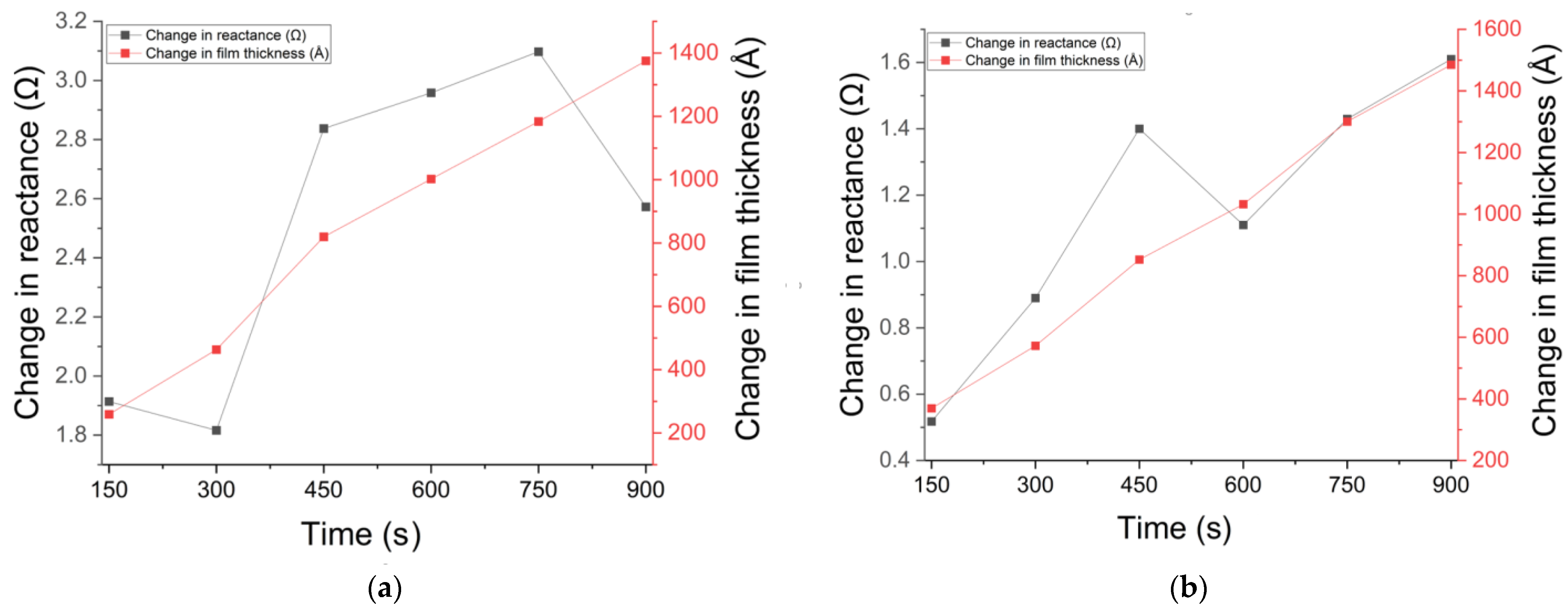
As shown in Figure 10a, the change in reactance in Experiment 1 (w/o cleaning) was slightly different. This means that in Experiment 1 (w/o cleaning), the correlation with the deposition thickness on the wafer was low. Additionally, as shown in Figure 10b, the correlation was usually high in Experiment 1 (one cleaning). The result of increased correlation of thin film deposited on the wafer supports our observation, and can be inferred by Equations (27) and (30). For one cleaning, d dep , wafer (> or ≈) d dep , wall , as shown in Equation (30), reactance includes the deposition thickness of the wafer. For w/o cleaning, d dep , wafer >> d dep , wall , as in Equation (27), the reactance is expressed only as a factor for the wall.
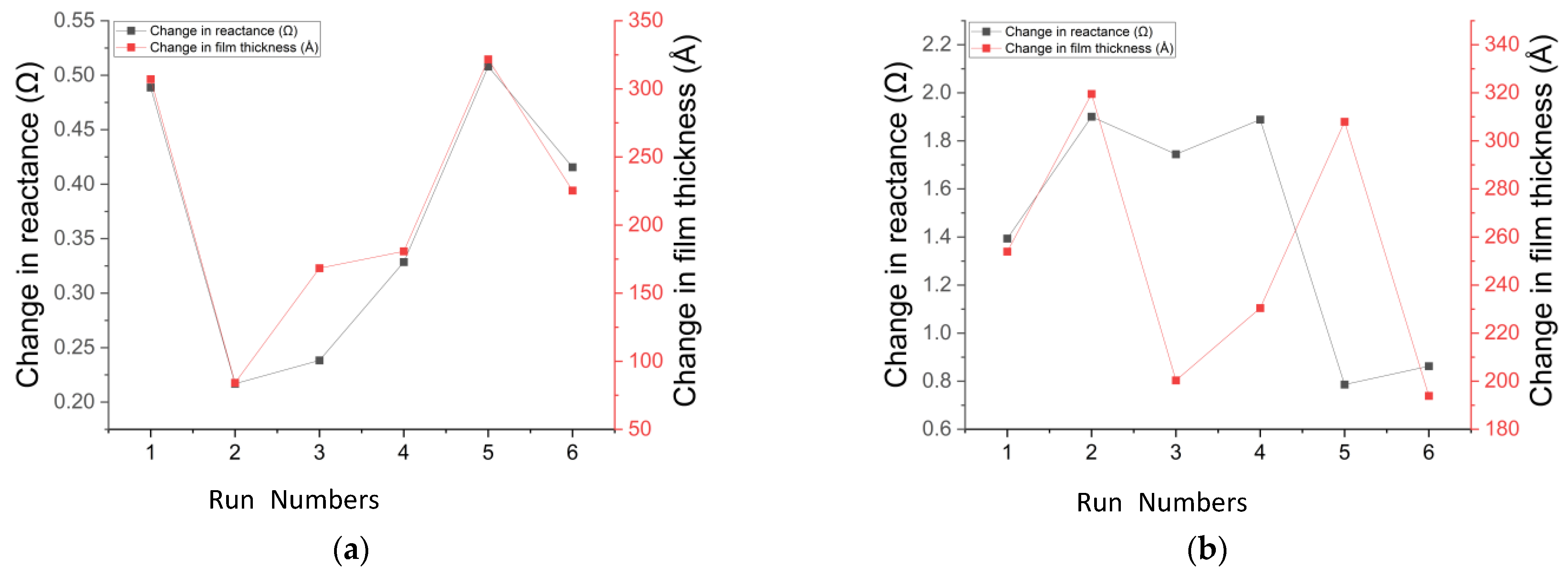
Figure 11a is the result of comparing the changes in the reactance in Experiment 2. The processing time was relatively short, at 150 s. Experiment 2 had a shorter deposition time and less chamber contamination than Experiment 1. Therefore, the correlation was high in the case of Experiment 2 (one cleaning) because there were few chamber contaminants. In Figure 11b, the correlations are shown to have been low for Experiment 2 (w/o cleaning), as expected.

5. Conclusions

The deposition thickness of the oxide film was monitored in situ during the deposition using Z-scan in a CCP-type 6-inch PECVD. The experiment was conducted by changing the deposition time without changing the recipe for a constant sheath thickness. In addition, Experiment 1: time split test and Experiment 2: 150 s reproducibility tests were conducted. The effect of one cleaning or w/o cleaning was also observed in each experiment. This study assumed a constant sheath thickness in the analysis model.
The sheath thickness calculated through the circuit model and the collision Child–Langmuir model was constant for the same process. In addition, it was confirmed that the reproducibility of the reactance was slightly low. However, this was due to the moisture absorption by the chamber opening and deposition on the wall and the showerhead. In addition, the change in the deposition thickness on the wafer was exponential, but the change in reactance was linear. Therefore, other factors that increase reactance with time in the chamber were considered. The model was modified by adding deposition effects on the chamber walls or the showerhead. When the modified circuit model was analyzed, the reactance was greatly affected by the deposition of the wall and the showerhead. To prove this, one cleaning and w/o cleaning were analyzed. In general, one cleaning showed a higher correlation than w/o cleaning. Therefore, the conditions of the wall and the showerhead were important for impedance monitoring. As a result, the effect of reactance change in the chamber was analyzed, and limited deposition thickness monitoring was possible. Through this study, it is predicted that wall and showerhead deposition monitoring will be possible in a process using a long deposition time.

Author Contributions

Conceptualization, S.J.H.; experiment and analysis, H.K.P.; writing—original draft preparation, H.K.P. and W.S.S.; writing—review and editing, S.J.H.; visualization, H.K.P.; funding acquisition, S.J.H. All authors have read and agreed to the published version of the manuscript.

Funding

This research was supported by the Ministry of Trade, Industry and Energy (MOTIE; GID 1415182073) and the Korea Semiconductor Research Consortium (KSRC; GID 20022492) support program for the development of a future semiconductor device.

Institutional Review Board Statement

Not applicable.

Informed Consent Statement

Not applicable.

Data Availability Statement

Data presented in this study are available on request from the corresponding author. Data are not publicly available due to a restriction of the equipment supplier.

Acknowledgments

The authors are grateful to D.W. Shin of New Power Plasma for collaboration on the impedance analysis.

Conflicts of Interest

The authors declare no conflict of interest.

References

  1. Sahu, B.B.; Han, J.G.; Shin, K.S.; Hori, M. Nitrogen radical and plasma diagnostics in dual frequency hybrid plasmas to investigate N2/SiH4 PECVD process. Plasma Process. Polym. 2016, 13, 447–458. [Google Scholar] [CrossRef]
  2. Baek, G.; Baek, J.H.; Kim, H.M.; Lee, S.; Jin, Y.; Park, H.S.; Park, J.S. Atomic layer chemical vapor deposition of SiO2 thin films using a chlorine-free silicon precursor for 3D NAND applications. Ceram. Int. 2021, 47, 19036–19042. [Google Scholar] [CrossRef]
  3. Hopwood, J.; Guarnieri, C.R.; Whitehair, S.J.; Cuomo, J.J. Langmuir probe measurements of a radio frequency induction plasma. J. Vac. Sci. Technol. A Vac. Surf. Film. 1993, 11, 152–156. [Google Scholar] [CrossRef]
  4. Chung, C. Experimental investigation on the floating potential of cylindrical Langmuir probes in non-Maxwellian electron distributions. Phys. Plasmas 2005, 12, 123505. [Google Scholar] [CrossRef]
  5. Kang, G.J.; An, S.R.; Kim, K.; Hong, S.J. An in situ monitoring method for PECVD process equipment condition. Plasma Sci. Technol. 2019, 21, 064003. [Google Scholar] [CrossRef]
  6. Jang, D.B.; Hong, S.J. In-situ monitoring of multiple oxide/nitride dielectric stack PECVD deposition process. Trans. Electr. Electron. Mater. 2018, 19, 21–26. [Google Scholar] [CrossRef]
  7. Kim, S.J.; Lee, J.J.; Lee, Y.S.; Cho, C.H.; You, S.J. Crossing Frequency Method Applicable to Intermediate Pressure Plasma Diagnostics Using the Cutoff Probe. Sensors 2022, 22, 1291. [Google Scholar] [CrossRef] [PubMed]
  8. You, K.H.; You, S.J.; Kim, D.W.; Na, B.K.; Seo, B.H.; Kim, J.H.; Chang, H.Y. Measurement and analysis of electron-neutral collision frequency in the calibrated cutoff probe. Phys. Plasmas 2016, 23, 033509. [Google Scholar] [CrossRef]
  9. Bang, J.Y.; Yoo, K.; Kim, D.H.; Chung, C.W. A plasma diagnostic technique using a floating probe for the dielectric deposition process. Plasma Sources Sci. Technol. 2011, 20, 065005. [Google Scholar] [CrossRef]
  10. Lee, M.H.; Jang, S.H.; Chung, C.W. Floating probe for electron temperature and ion density measurement applicable to processing plasmas. J. Appl. Phys. 2007, 101, 033305. [Google Scholar] [CrossRef] [Green Version]
  11. Ogawa, D.; Nakamura, K.; Sugai, H. A novel technique for in-situ simultaneous measurement of thickness of deposited film and electron density with two curling probes. Plasma Sources Sci. Technol. 2020, 29, 075009. [Google Scholar] [CrossRef]
  12. Hotta, M.; Ogawa, D.; Nakamura, K.; Sugai, H. Real-time curling probe monitoring of dielectric layer deposited on plasma chamber wall. Jpn. J. Appl. Phys. 2018, 57, 046201. [Google Scholar] [CrossRef]
  13. Karkari, S.K.; Gaman, C.; Ellingboe, A.R.; Swindells, I.; Bradley, J.W. A floating hairpin resonance probe technique for measuring time-resolved electron density in pulse discharge. Meas. Sci. Technol. 2007, 18, 2649. [Google Scholar] [CrossRef]
  14. Arshadi, A.; Brinkmann, R.P.; Hotta, M.; Nakamura, K. A simple and straightforward expression for curling probe electron density diagnosis in reactive plasmas. Plasma Sources Sci. Technol. 2017, 26, 045013. [Google Scholar] [CrossRef]
  15. Roh, H.; Ryu, S.; Jang, Y.; Kim, N.; Jin, Y.; Park, S.; Kim, G. Development of the virtual metrology for the nitride thickness in multi-layer plasma-enhanced chemical vapor deposition using plasma-information variables. IEEE Trans. Semicond. Manuf. 2018, 31, 232–241. [Google Scholar] [CrossRef]
  16. Hong, S.J.; May, G.S.; Park, D.C. Neural network modeling of reactive ion etching using optical emission spectroscopy data. IEEE Trans. Semicond. Manuf. 2003, 16, 598–608. [Google Scholar] [CrossRef]
  17. Kwon, H.; Hong, S.J. Use of Optical Emission Spectroscopy Data for Fault Detection of Mass Flow Controller in Plasma Etch Equipment. Electronics 2022, 11, 253. [Google Scholar] [CrossRef]
  18. Kim, D.H.; Hong, S.J. Use of plasma information in machine-learning-based fault detection and classification for advanced equipment control. IEEE Trans. Semicond. Manuf. 2021, 34, 408–419. [Google Scholar] [CrossRef]
  19. Choi, J.E.; Hong, S.J. Machine learning-based virtual metrology on film thickness in amorphous carbon layer deposition process. Meas. Sens. 2021, 16, 100046. [Google Scholar] [CrossRef]
  20. Oyama, K.I.; Lee, C.H.; Fang, H.K.; Cheng, C.Z. Means to remove electrode contamination effect of Langmuir probe measurement in space. Rev. Sci. Instrum. 2012, 83, 055113. [Google Scholar] [CrossRef]
  21. Sahu, B.B.; Han, J.G.; Hori, M.; Takeda, K. Langmuir probe and optical emission spectroscopy studies in magnetron sputtering plasmas for Al-doped ZnO film deposition. J. Appl. Phys. 2015, 117, 023301. [Google Scholar] [CrossRef]
  22. Naz, M.Y.; Ghaffar, A.; Rehman, N.U.; Azam, M.; Shukrullah, S.; Qayyum, A.; Zakaullah, M. Symmetric and Asymmetric Double Langmuir Probes Characterization of Radio Frequency Inductivley Coupled Nitrogen Plasma. Prog. Electromagn. Res. 2011, 115, 207–221. [Google Scholar] [CrossRef] [Green Version]
  23. Kim, I.J.; Yun, I. Real-time plasma uniformity measurement technique using optical emission spectroscopy with revolving module. IEEE Sens. J. 2018, 19, 2356–2361. [Google Scholar] [CrossRef]
  24. Kim, B.; Im, S.; Yoo, G. Performance evaluation of CNN-based end-point detection using in-situ plasma etching data. Electronics 2020, 10, 49. [Google Scholar] [CrossRef]
  25. Kim, M.W.; Kim, S.G.; Zhao, S.; Hong, S.J.; Han, S.S. Endpoint detection in plasma etching using principal component analysis and expanded hidden markov model. ECS Trans. 2011, 34, 943. [Google Scholar] [CrossRef]
  26. Kim, J.; Lee, K.I.; Jeong, H.Y.; Lee, J.H.; Choi, Y.S. Anti-contamination SMART (Spectrum Monitoring Apparatus with Roll-to-roll Transparent film) window for optical diagnostics of plasma systems. Rev. Sci. Instrum. 2021, 92, 013507. [Google Scholar] [CrossRef]
  27. Jang, H.; Nam, J.; Kim, C.K.; Chae, H. Real-Time Endpoint Detection of Small Exposed Area SiO2 Films in Plasma Etching Using Plasma Impedance Monitoring with Modified Principal Component Analysis. Plasma Process. Polym. 2013, 10, 850–856. [Google Scholar] [CrossRef]
  28. Oh, S.-J.; Sung, D.-Y.; Ko, J.-M.; Nam, S.K. Improving Detection of Plasma Etching End Point Using Light Compensation on Optical Emission Spectra. J. Vac. Sci. Technol. B 2022, 40, 052206. [Google Scholar] [CrossRef]
  29. Stancu, G.D.; Leroy, O.; Coche, P.; Gadonna, K.; Guerra, V.; Minea, T.; Alves, L.L. Microwave air plasmas in capillaries at low pressure II. Experimental investigation. J. Phys. D Appl. Phys. 2016, 49, 435202. [Google Scholar] [CrossRef]
  30. Yeom, H.J.; Kim, J.H.; Choi, D.H.; Choi, E.S.; Yoon, M.Y.; Seong, D.J.; Lee, H.C. Flat cutoff probe for real-time electron density measurement in industrial plasma processing. Plasma Sources Sci. Technol. 2020, 29, 035016. [Google Scholar] [CrossRef]
  31. Godyak, V.A.; Piejak, R.B.; Alexandrovich, B.M. Electron energy distribution function measurements and plasma parameters in inductively coupled argon plasma. Plasma Sources Sci. Technol. 2002, 11, 525. [Google Scholar] [CrossRef]
  32. Bora, B.; Bhuyan, H.; Favre, M.; Wyndham, E.; Chuaqui, H. Diagnostic of capacitively coupled radio frequency plasma by homogeneous discharge model. Phys. Lett. A 2012, 376, 1356–1359. [Google Scholar] [CrossRef]
  33. Seong, I.; Kim, S.; Lee, Y.; Cho, C.; Lee, J.; Jeong, W.; You, S. Development of a Noninvasive Real-Time Ion Energy Distribution Monitoring System Applicable to Collisional Plasma Sheath. Sensors 2022, 22, 6254. [Google Scholar] [CrossRef]
  34. Chabert, P.; Braithwaite, N. Physics of Radio-Frequency Plasmas, 1st ed.; Cambridge University Press: New York, NY, USA, 2011; pp. 142–154. [Google Scholar]
  35. Lieberman, M.A.; Lichtenberg, A.J. Principles of Plasma Discharges and Materials Processing, 2nd ed.; John Wiley & Sons: Hoboken, NJ, USA, 2005; p. 399. [Google Scholar]
  36. Choi, S.Y.; White, J.M. Large Area PECVD Technology. ECS Trans. 2009, 25, 701. [Google Scholar] [CrossRef]
  37. Benilov, M.S. The Child–Langmuir law and analytical theory of collisionless to collision-dominated sheaths. Plasma Sources Sci. Technol. 2008, 18, 014005. [Google Scholar] [CrossRef]
  38. Lieberman, M.A. Dynamics of a collisional, capacitive RF sheath. IEEE Trans. Plasma Sci. 1989, 17, 338–341. [Google Scholar] [CrossRef]
  39. Lisovskiy, V.; Yegorenkov, V.; Artushenko, E.; Booth, J.P.; Martins, S.; Landry, K.; Cassagne, V. Normal regime of the weak-current mode of an rf capacitive discharge. Plasma Sources Sci. Technol. 2012, 22, 015018. [Google Scholar] [CrossRef]
  40. Mutsukura, N.; Kobayashi, K.; Machi, Y. Plasma sheath thickness in radio-frequency discharges. J. Appl. Phys. 1990, 68, 2657–2660. [Google Scholar] [CrossRef]
  41. Kasashima, Y.; Fumihiko, U. Monitoring of Condition of Deposited Film Causing Particles in Plasma Etching by Using Practical Load Impedance Monitoring Method. J. Vac. Soc. Jpn. 2016, 59, 270–275. [Google Scholar] [CrossRef]
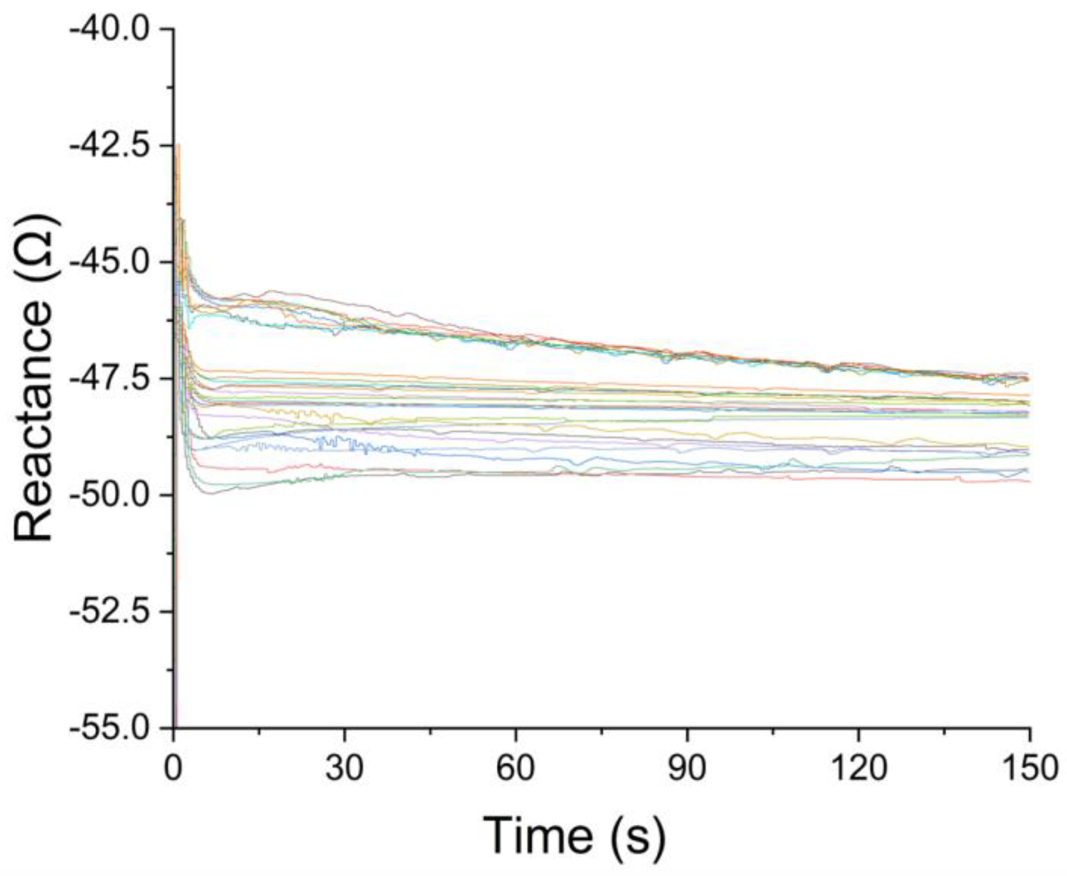
Figure 1. Repeatability test data for plasma reactance acquired from the VI probe over 30 consecutive runs.
Coatings 13 00559 g001
Figure 2. Plasma equivalent circuit model.
Coatings 13 00559 g002
Figure 3. (a) Experimental schematic and (b) simplified impedance model.
Coatings 13 00559 g003
Figure 4. Plasma circuit model used for VI probe analysis.
Coatings 13 00559 g004
Figure 5. Calculated sheath thickness; (a) Experiment 1 and (b) Experiment 2.
Coatings 13 00559 g005
Figure 6. Calculated reactance; (a) Experiment 1 with one cleaning, (b) Experiment 1 without chamber cleaning, (c) Experiment 2 with one cleaning, and (d) Experiment 2 without chamber cleaning.
Coatings 13 00559 g006
Figure 7. Experiment 1: film thickness on wafer (w/o cleaning).
Coatings 13 00559 g007
Figure 8. An example of a contaminated CVD chamber: (a) wall deposition and (b) showerhead. (Image directly acquired from the university laboratory environment with heavily contaminated condition).
Coatings 13 00559 g008
Figure 9. Modified equivalent circuit (wall and showerhead).
Coatings 13 00559 g009
Figure 10. Experiment 1: comparison of change in reactance and film thickness (a) without chamber cleaning and (b) with one chamber cleaning.
Coatings 13 00559 g010
Figure 11. Experiment 2: comparison of change in reactance and film thickness (a) without chamber cleaning and (b) with one chamber cleaning.
Coatings 13 00559 g011
Table 1. Experiment condition.
ConditionDepositionCleaning
SiH4 (sccm)9-
NF3 (sccm)-40
N2O (sccm)25-
Ar (sccm)-5
Pressure (mTorr)5001000
Power (W)300300
Temp (°C)200200
Table 2. Experiments 1 (time increment) and 2 (150 s reproducibility).
Experiment 1 (Time Increment)Experiment 2 (150 s Reproducibility)
150 sNo. 1 (150 s)
300 sNo. 2 (150 s)
450 sNo. 3 (150 s)
600 sNo. 4 (150 s)
750 sNo. 5 (150 s)
900 sNo. 6 (150 s)
Disclaimer/Publisher’s Note: The statements, opinions and data contained in all publications are solely those of the individual author(s) and contributor(s) and not of MDPI and/or the editor(s). MDPI and/or the editor(s) disclaim responsibility for any injury to people or property resulting from any ideas, methods, instructions or products referred to in the content.