Abstract
In our work, the model of self-consistent electron–deformation–diffusion effects in thin films grown on substrate with the mismatch of lattice parameters of the contacting materials is constructed. The proposed theory self-consistently takes into account the interaction of the elastic field (created by the mismatch of lattice parameters of the film and the substrate, and point defects) with the diffusion processes of point defects and the electron subsystem of semiconductor film. Within the framework of the developed model, the spatial distribution of deformation, concentration of defects, conduction electrons and electric field intensity is investigated, depending on the value of the mismatch, the type of defects, the average concentrations of point defects and conduction electrons. It is established that the coordinate dependence of deformation and the concentration profile of defects of the type of stretching (compression) centers, along the axis of growth of the strained film, have a non-monotonic character with minima (maxima), the positions of which are determined by the average concentration of point defects. It is shown that due to the electron–deformation interaction in film with a lattice parameter mismatch, the spatial redistribution of conduction electrons is observed and n-n+ transitions can occur. Information about the self-consistent spatial redistribution of point defects, electrons and deformation of the crystal lattice in semiconductor materials is necessary for understanding the problems of their stability and degradation of nano-optoelectronic devices operating under conditions of intense irradiation.
1. Introduction
Thin films are widely used in the production of discrete semiconductor devices and integrated microcircuits [1], as well as in the production of photo templates (the main technological tool of microelectronics). The obtained high-quality thin film layers that are reproducible in terms of electrophysical parameters are one of the most important technological processes of forming the structures of both discrete diodes and transistors [2], as well as active and passive elements of integrated microcircuits [3].
The process of manufacturing films is usually accompanied by the occurrence of internal strains in the films and substrates, which can change the properties of the films themselves.
In most cases, the main reasons for the occurrence of internal strains are changes in the volume of the films during their formation [4], different coefficients of thermal expansion of the material of the film and substrate [5,6], as well as different lattice parameters of the film and substrate [7,8]. The magnitude and signs of mechanical deformations in the films depend on many factors that are related to the methods of applying the films to the substrate and the character of their growth. In particular, during heteroepitaxial growth, the deformation mainly occurs due to the mismatch of lattice parameters of the contacting materials (film and substrate). The intrinsic point defects (interstitial atoms and vacancies) and foreign impurities, which can be both stretching and compressive centers, are another important source of elastic deformation in films. The concentration of impurities, interstitial atoms and vacancies, the depth of their placement and, accordingly, the magnitude of mechanical strain and its distribution in semiconductor film depend significantly on the methods and conditions in which the film is obtained. However, in general, mechanical deformation is defined as the sum of the two deformations mentioned above: the mismatch between lattice parameters of the film and the substrate and the deformation created by point defects. Moreover, these factors are self-consistent with each other. The nonuniform deformation that occurs due to the mismatch induces a flow of defects, which are also centers of deformation and accumulate in different areas of the film depending on the sign of the deformation that they create.
It is known that the optical and electrical properties of semiconductor devices depend, to a large extent, on both the deformation of the lattice and the spatial distribution of point defects. The interaction of defects with the deformation field created both by the mismatch of crystal lattices of the contacting materials and by point defects causes the spatial redistribution of the latter. This can lead to both the accumulation and reduction of the number of defects in the active area, depending on the character of deformation [9,10].
In [11], a model is developed that describes the change in the diffusion process under the influence of various types of deformation. In [12], the theoretical investigation of defect redistribution taking into account their non-zero volume on the basis of the stationary diffusion equation is carried out in linear approximation. In the same work, it is shown that the deformation flow opposes the diffusion flow and under certain conditions can exceed it. However, this model does not take into account the effects caused by the non-local interaction between defects and matrix atoms. The authors of [13] developed the mathematical model of diffusion in layered materials, which can be used for thin films. However, this model does not take into account the influence of deformation caused by the non-zero volume of defects on their diffusion. It is shown in [14] that an increase in mechanical strain caused by the mismatch of lattice parameters leads to a change in the band structure of InxGa1−xN/GaN, which manifests itself in a shift of the electroluminescence intensity maximum. Currently, the mathematical models of the piezoelectric elastic-semiconductor medium have been developed, taking into account photothermal effects [15], and the complex influence of laser irradiation and magnetic fields within the photo-thermoelastic model have also been theoretically investigated [16]. However, these models are limited only to a uniform medium. The presence of nonuniform deformation in semiconductor film leads to a spatial redistribution of conduction electrons and the emergence of an electric field due to a self-consistent electron–deformation coupling. The specific features of diffusion in semiconductors are largely determined by the interaction of implanted impurities and lattice defects with the electron subsystem. This interaction is manifested, firstly, by a change in the concentration of defects; secondly, in a redistribution of conduction electrons and a change in the concentration profile of implanted impurities; and, thirdly, in the existence of an internal electric field created by nonuniform distributed impurity ions and electrons. Therefore, the information about the spatial distribution of defect concentration, the crystal lattice parameter, the spatial redistribution of conduction electrons, and the electrostatic potential is important for the predicted control of the physical parameters of semiconductor films.
In this work, the model of semiconductor film with the significant mismatch of lattice parameters relative to the substrate is developed, taking into account the self-consistent coupling between the elastic field (created by the mismatch of lattice parameters of the contacting materials and point defects), the point defect diffusion, and the electron subsystem.
2. The Model of Self-Consistent Deformation–Diffusion Phenomena in Stressed Film
Let point defects (implanted impurities, vacancies and interstitial atoms) with an average concentration of Nd0i are distributed in a stressed epitaxial layer, grown-up on a thick substrate (hs >> h0, where hs, h0 are the thickness of the substrate and the grown-up layer, respectively). Due to the mismatch of lattice parameters of the contacting materials of the substrate and the grown-up layer, the deformation ε(x) occurs in the grown-up layer. The x-axis is directed in the direction of film growth, and the starting point is chosen at the film–substrate heteroboundary. Since we are considering a thick substrate compared with a film, the deformation of the substrate itself can be neglected [17]. The maximum deformation of the film will be at the film–substrate heteroboundary, which is determined by the difference in lattice parameters of the contacting materials. With the distance from the heteroboundary in the direction of the growth axis, the lattice deformation decreases and is modeled by an exponential function [18]:
where ε0 is the relative change in the elementary cell volume of the grown-up layer at the heteroboundary [17]:
where , , are the deformation tensor components of the epitaxial layer material; as, a0 are the lattice parameters of the substrate and epitaxial layer, respectively; C11, C12 are the elastic constants of the epitaxial layer material; and γ is a quantity that is inverse to the effective shielding radius of the deformation field, which depends both on the material elastic constants and on the average point defect concentration.
The self-consistent interaction of the point defect system with the elastic medium of the epitaxial layer leads to the renormalization of deformation and the spatial redistribution of moving point defects with a concentration of .
In this work, the expression for the free energy density of the nonuniform strained epitaxial layer with point defects in the direction of the growth axis, within the elastic continuum, without taking into account anharmonic terms, is represented as [19]:
where is the renormalized epitaxial layer deformation; ρ is medium density; is the longitudinal velocity of sound; is the deformation potential; K is the module of comprehensive compression; is the change in crystal volume when one defect is created; is the characteristic length of interaction of defects with structure atoms; T is the temperature; S is the entropy of the system; and indices i = 1, 2, …, k correspond to the type of point defect. The first term determines the elastic energy density of the film with the mismatch of lattice parameters of the contacting materials, which contains point defects. The second and third terms are the energy density of the interaction of defects with the elastic medium and the nonlocal interaction with lattice atoms [19].
The mechanical strain in the epitaxial layer, created both by point defects and by the mismatch of lattice parameters of the materials of the epitaxial layer and the substrate, has the form:
Using the continuity equation
We write the equation for the renormalized deformation in the form:
Since the defect diffusion occurs in the deformation field created both by the mismatch of lattice parameters of the substrate material and the epitaxial layer, and by the spatial redistribution of point defects (interstitial atoms and vacancies), then the usual diffusion flow
which is determined only by the magnitude and direction of the concentration gradient, is superimposed on the induced deformation flow of defects [19]
This component of defect flow is due to the emergence of additional forces from the nonuniform elastic field. The second term takes into account nonlocal Hooke’s law (the nonlocality of the interaction of defects with film atoms through the elastic field). The detailed derivation of this formula is presented in [19].
Then, the equation for the defect concentration (interstitial atoms or vacancies) will be written in the form:
where Ddi is the point defect diffusion coefficient; Gdi is the rate of defect generation; and is the lifetime of the defect.
Next, we consider the stationary state of such a defect–deformation system, i.e.,: , .
Let us represent the lattice deformation and the defect concentration in the form:
Here, is the spatially averaged value of lattice deformation:
where L is the epitaxial layer thickness; and and are the spatially nonuniform components of lattice deformation of the epitaxial layer and the point defect concentration, respectively.
Neglecting the recombination of interstitial atoms and vacancies (), we obtain a coupled system of equations for the point defect diffusion and the epitaxial layer deformation:
Integrating the differential Equation (13), we find the distribution of the point defect concentration:
The latter equality holds under the condition:
The integration constant is chosen for the following reasons. In this case, if the nonuniform component of the deformation parameter is equal to zero, then the point defect concentration should be close to its spatially uniform value of Nd0i. The epitaxial layer contains interstitial atoms and vacancies, but, as a rule, the deformation potential of interstitial atoms is much greater than the deformation potential of vacancies () [10]. Therefore, in Equation (6) for self-consistent deformation, we will neglect the contribution of vacancies. In the future, we will limit ourselves to one type of defect in the semiconductor film (interstitial atom or foreign impurity). This approximation is valid in the case when the value of is much larger for one type of defect than for the others. Substituting (15) into (14), we obtain
where
Since the solution of Equation (17) must be finite at x→∞, therefore one of the integration constants is equal to zero. Then the solution of Equation (17) (Nd0 < Ndc), taking into account the additional condition
has the form:
The parameter γ determines the rate of reduction of deformation, which occurs due to the mismatch of lattice parameters of the substrate materials and the grown-up layer, with distance from the heteroboundary. The parameter γ is found from the condition of minimum free energy
where is the free energy of the epitaxial layer with volume V; and S is the surface area of the grown-up layer.
In the limiting cases, when , the deformation (19) , and the point defect concentration approaches the spatially uniform distribution (). In the case of the absence of defects () in the crystal, the deformation is created only due to the mismatch of the parameters of the crystal lattices of the substrate and the epitaxial layer , and in the absence of the mismatch of the lattice parameters at the heteroboundary , the deformation () is caused only by point defects.
3. The Self-Consistent Electron–Deformation–Diffusion Effects in Semiconductor Film
The self-consistent spatial redistribution of defects leads to the occurrence of nonuniform deformation, which is caused both by the mismatch of lattice parameters of the epitaxial layer and the substrate, and by the defects themselves (see Formula (19)). This, in turn, as result of self-consistent electron–deformation coupling, leads to the local displacement of the edges of the allowed bands and the electrochemical potential [20], which, taking into account the deformation [17,21], will take the form:
where m is the effective mass of electron in semiconductor film; n(x) is the electron concentration; and ac is the constant of deformation potential of the conduction band.
Consider a semiconductor film that contains electrons with an average concentration n0 and slow-moving ionized donors with an average concentration Nd0. According to the condition of electroneutrality, the following condition is fulfilled: n0 = Nd0.
From Formula (18), we obtain an expression for the electron concentration:
Then, in the linear approximation where the electron concentration can be determined as follows
where . By supplementing this equation with Poisson’s equation, we obtain a closed system of Equations (13), (17), (20) and (21) with an additional condition . By supplementing this equation with Poisson’s equation
we obtain a closed system of Equations (15), (19), (23) and (24) with an additional condition . Here, εd is the dielectric constant of the film material. Thus, we obtain an expression for the electrostatic potential, the electric field strength F(x) and the conduction electron concentration in the vicinity of the semiconductor film–substrate strained heteroboundary with the mismatch of lattice parameters of the contacting materials:
where , .
The mismatch of lattice parameters in the vicinity of the heteroboundary leads first to the spatial redistribution of defects and conduction electrons, and then, accordingly, to the emergence of an internal electric field. Such an effect is the reason for the emergence of another source of mechanical strain (due to the presence of a nonuniform electric field), caused by an electron–deformation interaction. This deformation can be calculated by the formula [22]:
where ν, E are the Poisson’s ratio and the Young’s modulus of film, respectively; and S is the surface area of film.
4. Results and Discussion
Figure 1 shows the results of calculating the coordinate dependence of crystal lattice deformation of the InAs film on the GaAs substrate (Figure 1a,b) and the Ge film on the Si substrate (Figure 1c,d) with interstitial atoms (Figure 1a,c) (θd = 10 eV > 0) and substitution impurities with a smaller ionic radius (Figure 1b,d) (θd = −5 eV < 0) at different values of the average defect concentration. The film parameters and the mismatch of lattice parameters of the film and the substrate are given in Table 1 [23,24,25].
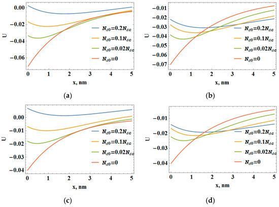
Figure 1.
The coordinate dependence of the deformation of the crystal lattice of the InAs film on the GaAs substrate (a,b) and the Ge film on the Si substrate (c,d) with interstitial atoms (a,c) and substitution impurities with a smaller ionic radius (b,d) at different values of the average concentration defects.

Table 1.
Some physical parameters of the film materials.
As we can see, such dependences have the non-monotonic character with minima, the positions of which are determined by the average point defect concentration Nd0. As the value of Nd0 increases, the position of the minima of lattice deformation of the epitaxial layer moves away from the heteroboundary. Both the deformation and the spatial redistribution of point defects are determined by two self-consistent competing factors: the component of deformation that arises due to the mismatch of lattice parameters of the substrate and the film, and the component of deformation induced due to the spatial redistribution of point defects. Near the heteroboundary, the main role is played by the compression deformation caused by the mismatch between the lattice parameters of the substrate and the film, which monotonically decreases in absolute value with distance from the heteroboundary (Figure 1).
Therefore, a monotonous decrease in the interstitial atom concentration is observed near the film–substrate contact (Figure 2a,b).
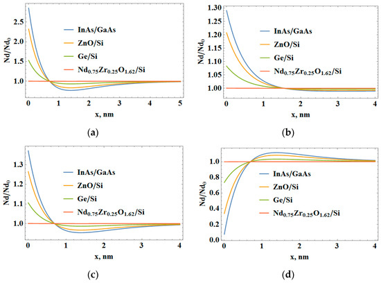
Figure 2.
The spatial redistribution of point defects for their different types and for their different average concentration values: (a) θd = 10 eV, Nd0 = 0.1Ndc; (b) θd = 10 eV, Nd0 = 0.8 Ndc; (c) θd = 5 eV, Nd0 = 0.1 Ndc; (d) θd = −5 eV, Nd0 = 0.8 Ndc.
At a distance x > 1.4 nm, the main contribution to the film deformation is made by the component arising due to the spatial redistribution of point defects. This leads to an increase in the stretching deformation of the crystal lattice of the epitaxial layer and, accordingly, to an increase in the value of the interstitial atom concentration, which approaches the corresponding average value of the defect concentration.
The Nd0.75Zr0.25O1.62 film on the Si substrate is chosen for comparison as a reference, since in such an epitaxial layer there is no mismatch of its lattice parameter with the silicon substrate [26].
There is a range of defect concentrations at which the deformation character of the material of the Ge film grown on the Si substrate near the heteroboundary changes to the opposite: from compression to stretching. This is explained by the fact that the growing layer near the heteroboundary is enriched with interstitial atoms (θd > 0, Figure 2a–c), which leads to an increase in the crystal lattice volume in comparison with the structure without point defects.
In compressed films (the lattice parameter of the film is greater than in the substrate), the interstitial atoms accumulate near the boundary and, on the contrary, their concentration decreases with distance from it. Such an effect was observed in experimental work [27] on the research of photoluminescence spectra of heterostructures, where it was shown that strained GaAs/InGaAs heterolayers delay the diffusion of hydrogen and defects into the crystal volume.
When foreign atoms are introduced into the film, not only additional interstitial defects appear, but also substitution atoms. In this case, depending on the ratio between the ionic radii of the film atom and the substitution impurity, both stretching and compressive deformation may occur.
Figure 1b,d and Figure 2d show the coordinate dependence of the crystal lattice deformation along the growth axis of film, which contains point defects (substitution impurities with an ionic radius smaller than the ionic radius of the film atoms (θd < 0)) and their spatial redistribution in the self-consistent deformation field. In this case, the point defects of the type of compression centers accumulate at a distance x > 1 nm from the heteroboundary, and near it there is a decrease in the concentration of defects in comparison with their spatially uniform distribution, which ultimately leads to an increase in the crystal lattice volume compared with defect-free layers.
The penetration depth of impurities depends significantly on the energy of these particles and their diffusion coefficient in the film material. However, even with low diffusion properties, the impurities can be deeply embedded due to the creation of their deformation flow [28]. The deformation flow occurs in the presence of a deformation gradient and is proportional to its magnitude. In the case of films obtained on the substrate, at the initial stage, the deformation flow of defects occurs, which is caused by the deformation gradient that arises due to the mismatch of lattice parameters of the film–substrate contacting materials. In addition, depending on the sign of the deformation potential of defects, their accumulation occurs in one or another area.
At the next stage, the deformation is the result of the self-consistent action of the heteroboundary, the defects themselves, which are also the centers of deformation, and the electron–deformation interaction of the elastic field with the electron subsystem. The deformation due to electron–deformation effects occurs as result of the existence of the nonuniform internal electric field.
Figure 3 and Figure 4 show the spatial distribution of electron concentration and electric field in semiconductor films obtained on substrates with the significant mismatch of lattice parameters.
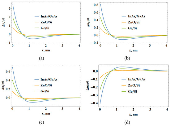
Figure 3.
The spatial redistribution of the concentration of conduction electrons in the presence of various types of defects and at different average values of the electron concentration: (a) θd = 10 eV, n0 = 1020 cm−3; (b) θd = 10 eV, n0 = 1018 cm−3; (c) θd = 5 eV, n0 = 1018 cm−3; (d) θd = −5 eV, n0 = 1018 cm−3.
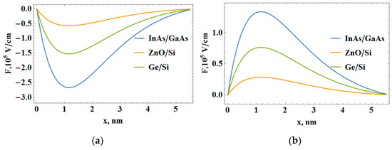
Figure 4.
The coordinate dependence of the electric field in semiconductor film in the case of the presence of point defects: (a) the defects of the type of stretching centers (θd = 10 eV); (b) the defects of the type of compression centers (θd = −5 eV).
Such a profile of electrons in the vicinity of the heteroboundary is mainly determined by the deformation character. In the area where defects of the type of stretching centers (θd > 0) are localized, the greater lowering of the bottom of the conduction band is observed, which contributes to the localization of electrons near the boundary with the substrate (Figure 3a–c). Conversely, in the case of defects of the type of compression centers, near the heteroboundary, the concentration of electrons decreases compared with the average value (Figure 3d). That is, due to self-consistent electron–deformation coupling, an n-n+ transition occurs in the vicinity of the film–substrate boundary.
An increase in the average electron concentration (Figure 3a,b) leads to their greater localization near the heteroboundary in the case of defects of the type of stretching centers. In addition, important factors for the redistribution of the electron density are the mismatch of lattice parameters and the magnitude of deformation potential of the conduction band (Δn ~ acε0). That is why the InAs film obtained on the GaAs substrate is the most effective among the considered materials for the formation of n-n+ transitions under the influence of laser irradiation (the large interstitial atom concentration is generated). The ZnO film on the Si substrate has a rather large mismatch, but a much smaller constant of deformation potential of the conduction band (see Table 1).
This conduction electron redistribution leads to the emergence of a nonuniform electric field, the character of which depends on the type of defects (Figure 4).
The nonuniform electric field is the source of another type of deformation caused by electron–deformation interaction (Formula (27)). In the area where a decrease in the electric field intensity is observed, we have an accumulation of electron density and the emergence of “electron–deformation compression”. In the case of defects of stretching centers, as result of self-consistent electron–deformation interaction, the additional compression occurs near the film–substrate heteroboundary. On the contrary, in the presence of defects of the type of compression centers, near the heteroboundary, the electron–deformation interaction leads to a partial compensation of the mismatch in the lattice parameter of the film compared with the substrate. The conducted calculations show that the semiconductor film can be conditionally divided into three parts: (1) the layer enriched in defects of the type of stretching centers and electrons near the heteroboundary with the substrate (or the layer depleted by defects of the type of compression centers and electrons near the heteroboundary with the substrate); (2) the layer with an inverse distribution of defects and electrons at some distance from the heteroboundary; and (3) the area with a concentration of defects and electrons close to a uniform distribution.
This effect was found in experimental work [29], where it was shown that both the InAs and InSb films grown on the GaAs substrate, actually have a three-layer structure at low temperatures.
The effects investigated above are significant when the deformation flow of defects caused by the deformation gradient is commensurate with the normal diffusion flow caused by the concentration gradient of defects. As the temperature decreases, the role of deformation flows increases compared with diffusion flows.
5. Conclusions
Based on the self-consistent system of equations, i.e., the diffusion equation, the continuity equation and the Poisson’s equation, a theory is developed that describes electron–deformation–diffusion effects in semiconductor films with a significant lattice parameter mismatch.
Within the framework of the proposed model, it is established that the semiconductor film can be conditionally divided into three parts: (1) the layer enriched in defects of the type of stretching centers and electrons near the heteroboundary with the substrate (or the layer depleted by defects of the type of compression centers and electrons near the heteroboundary with the substrate); (2) the layer with an inverse distribution of defects and electrons at some distance from the heteroboundary; and (3) the area with a concentration of defects and electrons close to a uniform distribution.
It is shown that, due to the electron–deformation interaction in film with a lattice parameter mismatch, the spatial redistribution of conduction electrons is observed and n-n+ transitions can occur. An increase in the average electron concentration leads to their greater localization near the film–substrate boundary (the film undergoes compressive deformation due to the lattice parameter mismatch) in the case of defects of the type of stretching centers. The obtained results can be the basis for the development of optimal methods of predicted nanostructuring of the semiconductor film surface using concentrated flows of energy (the generation of significant concentration of point defects), as well as the methods of predicting the behavior of optoelectronic materials that are used in extreme conditions. The proposed models can also be used to describe the prediction of mechanical behavior and degradation (destruction) of active elements of integrated microcircuits based on semiconductor films.
Author Contributions
Conceptualization, O.K.; methodology, O.D. and R.P.; software, Y.P.; validation, I.S., O.D. and Y.P.; formal analysis, R.P.; investigation, I.S. and O.K.; resources, O.K.; data curation, I.S. and O.D.; writing—original draft preparation, O.D.; writing—review and editing, O.K.; visualization, O.D. and Y.P.; supervision, I.S. All authors have read and agreed to the published version of the manuscript.
Funding
This research received no external funding.
Institutional Review Board Statement
Not applicable.
Informed Consent Statement
Not applicable.
Data Availability Statement
Not applicable.
Conflicts of Interest
The authors declare that they have no conflict of interest.
References
- Lo Nigro, R.; Fiorenza, P.; Greco, G.; Schilirò, E.; Roccaforte, F. Structural and Insulating Behaviour of High-Permittivity Binary Oxide Thin Films for Silicon Carbide and Gallium Nitride Electronic Devices. Materials 2022, 15, 830. [Google Scholar] [CrossRef] [PubMed]
- Virt, I. Special Issue: Recent Advances in Semiconducting Thin Films. Coatings 2023, 13, 79. [Google Scholar] [CrossRef]
- Kim, G.; Kim, D.; Choi, Y.; Ghorai, A.; Park, G.; Jeong, U. New Approaches to Produce Large-Area Single Crystal Thin Films. Adv. Mater. 2022; Online ahead of print. [Google Scholar] [CrossRef] [PubMed]
- Bajtošová, L.; Křivská, B.; Králík, R.; Veselý, J.; Hanuš, J.; Harcuba, P.; Fikar, J.; Yadav, A.; Cieslar, M. Deformation Mechanisms of Al Thin Films: In-situ TEM and Molecular Dynamics Study. Scr. Mater. 2022, 215, 114688. [Google Scholar] [CrossRef]
- Kang, C.W.; Huang, H. Deformation, Failure and Removal Mechanisms of Thin Film Structures in Abrasive Machining. Adv. Manuf. 2017, 5, 1–19. [Google Scholar] [CrossRef]
- Ritz, E.T.; Benedek, N.A. Strain Game Revisited for Complex Oxide Thin Films: Substrate-Film Thermal Expansion Mismatch in PbTiO3. Phys. Rev. Mater. 2020, 4, 084410. [Google Scholar] [CrossRef]
- Kumar, G.A.; Reddy, M.V.R.; Reddy, K.N. Structural and Optical Properties of ZnO Thin Films Grown on Various Substrates by RF Magnetron Sputtering. IOP Conf. Ser. Mater. Sci. Eng. 2015, 73, 012133. [Google Scholar] [CrossRef]
- Tsai, C.Y.; Lai, J.D.; Feng, S.W.; Huang, C.J.; Chen, C.H.; Yang, F.W.; Wang, H.C.; Tu, L.W. Growth and Characterization of Textured Well-Faceted ZnO on Planar Si(100), Planar Si(111), and Textured Si(100) Substrates for Solar Cell Applications. Beilstein J. Nanotechnol. 2017, 8, 1939–1945. [Google Scholar] [CrossRef]
- Kuzyk, O.V.; Dan’kiv, O.O.; Peleshchak, R.M.; Stolyarchuk, I.D. The Role of Deformation and Temperature Fields in the Distribution of Dot Defects and Modification of the Band Structure of ZnO Caused by Pulsed Laser Irradiation. Rom. Rep. Phys. 2022, 74, 502. [Google Scholar]
- Peleshchak, R.M.; Kuzyk, O.V.; Dan’kiv, O.O. The deformation-diffusion mechanism of the formation of n-n+ -transitions in semiconductors under the influence of pulsed laser irradiation. Rom. Rep. Phys. 2021, 73, 506. [Google Scholar]
- Robson, J.D. Deformation Enhanced Diffusion in Aluminium Alloys. Metall. Mater. Trans. A 2020, 51, 5401–5413. [Google Scholar] [CrossRef]
- Capello, L. Structural Investigation of Silicon after Ion-Implantation Using Combined X-ray Scattering Method; Université Claude Bernard: Lyon, France, 2005; 143p. [Google Scholar]
- Chernukha, O.; Chuchvara, A.; Bilushchak, Y.; Pukach, P.; Kryvinska, N. Mathematical Modelling of Diffusion Flows in Two-Phase Stratified Bodies with Randomly Disposed Layers of Stochastically Set Thickness. Mathematics 2022, 10, 3650. [Google Scholar] [CrossRef]
- Veleschuk, V.P.; Vlasenko, A.I.; Kisselyuk, M.P. On the Shift of the Electroluminescence Spectra of InxGa1−x N/GaN Structures with Various Indium Contents and Various Substrate Materials Caused by the Stark Effect and Mechanical Stresses. Semiconductors 2015, 49, 1007–1011. [Google Scholar] [CrossRef]
- Khamis, A.K.; Lotfy, K.; El-Bary, A.A.; Mahdy, A.M.S.; Ahmed, M.H. Thermal-Piezoelectric Problem of a Semiconductor Medium during Photo-Thermal Excitation. Waves Random Complex Media 2021, 31, 2499–2513. [Google Scholar] [CrossRef]
- Mahdy, A.M.S.; Lotfy, K.; El-Bary, A. Variable Thermal Conductivity and Hyperbolic Two-Temperature Theory during Magneto-Photothermal Theory of Semiconductor Induced by Laser Pulses. Eur. Phys. J. Plus 2021, 136, 651. [Google Scholar] [CrossRef]
- Van De Walle, C.G. Band Lineups and Deformation Potentials in the Model–Solid Theory. Phys. Rev. B 1989, 39, 1871–1883. [Google Scholar] [CrossRef]
- Sitnikova, A.A.; Bobyl, A.V.; Konnikov, S.G.; Ulin, V.P. Specific Features of Epitaxial-Film Formation on Porous III–V Substrates. Semiconductors 2005, 39, 523–527. [Google Scholar] [CrossRef]
- Balaban, O.V.; Grygorchak, I.I.; Peleshchak, R.M.; Kuzyk, O.V.; Dan’kiv, O.O. The Ultrasonic Modification of Thermodynamic and Kinetic Regularity of Lithium Intercalation in Talc. Prog. Nat. Sci. Mater. Int. 2014, 24, 397–404. [Google Scholar] [CrossRef]
- Shashkin, V.I.; Vostokov, N.V. Analytical Solution for Charge-Carrier Injection into an Insulating Layer in the Drift Diffusion Approximation. J. Appl. Phys. 2008, 104, 123708. [Google Scholar] [CrossRef]
- Peleshchak, R.M.; Kuzyk, O.V.; Dan’kiv, O.O. The Model of Nucleation of Nanometer Structure of the Adatoms Under the Action of Com-prehensive Pressure. J. Nano-Electron. Phys. 2018, 10, 01014. [Google Scholar] [CrossRef]
- Peleshchak, R.M.; Lazurchak, I.I.; Kuzyk, O.V.; Dan’kiv, O.; Zegrya, G.G. Role of Acoustoelectric Interaction in the Formation of Nanoscale Periodic Structures of Adsorbed Atoms. Semiconductors 2016, 50, 314–319. [Google Scholar] [CrossRef]
- Jemmy Cinthia, A.; Sudhapriyang, G.; Rajeswarapalanichamy, R.; Santhosh, M. Structural, Electronic and Elastic Properties of ZnO and CdO: A First-Principles Study. Procedia Mater. Sci. 2014, 5, 1034–1042. [Google Scholar] [CrossRef]
- Ohtake, A.; Mano, T.; Sakuma, Y. Strain Relaxation in InAs Heteroepitaxy on Lattice-Mismatched Substrates. Sci. Rep. 2020, 10, 4606. [Google Scholar] [CrossRef] [PubMed]
- Barhoumi, M. Third-Order Elastic Constants of Germanium and Silicon Using Adiabatic-Connection Fluctuation-Dissipation Theorem in Random Phase Approximation. Silicon, 2023; Online ahead of print. [Google Scholar] [CrossRef]
- Sreerama, J.L.; Zayasu, H.; Hamada, E.; Kawaguchi, T.; Sakamoto, N.; Shinozaki, K.; Suzuki, H.; Wakiya, N. Epitaxial Growth of Neodymia Stabilized Zirconia on Si(001) Substrate using Dynamic Aurora PLD. J. Ceram. Soc. Jpn. 2020, 128, 693–699. [Google Scholar] [CrossRef]
- Chen, Y.C.; Singh, J.; Bhattacharya, P.K. Suppression of Defect Propagation in Semiconductors by Pseudomorphic Layers. J. Appl. Phys 1993, 74, 3800–3804. [Google Scholar] [CrossRef]
- Abadias, G.; Colin, J.J.; Tingaud, D.; Djemia, P.; Belliard, L.; Tromas, C. Elastic Properties of α- and β-Tantalum Thin Films. Thin Solid Film. 2019, 688, 137403. [Google Scholar] [CrossRef]
- Okamoto, A.; Geka, H.; Shibasaki, I.; Yoshida, K. Transport Properties of InSb and InAs Thin Films on GaAs Substrates. J. Cryst. Growth 2005, 278, 604–609. [Google Scholar] [CrossRef]


Disclaimer/Publisher’s Note: The statements, opinions and data contained in all publications are solely those of the individual author(s) and contributor(s) and not of MDPI and/or the editor(s). MDPI and/or the editor(s) disclaim responsibility for any injury to people or property resulting from any ideas, methods, instructions or products referred to in the content. |
© 2023 by the authors. Licensee MDPI, Basel, Switzerland. This article is an open access article distributed under the terms and conditions of the Creative Commons Attribution (CC BY) license (https://creativecommons.org/licenses/by/4.0/).