Article

Studies on the Structure, Optical, and Electrical Properties of Doped Manganese (III) Phthalocyanine Chloride Films for Optoelectronic Device Applications

by
María Elena Sánchez Vergara
1,*,
María José Canseco Juárez
1,
Ricardo Ballinas Indili
2,
Genaro Carmona Reyes
2,
José Ramón Álvarez Bada
1 and
Cecilio Álvarez Toledano
2,*
1
Universidad Anáhuac México, Avenida Universidad Anáhuac 46, Col. Lomas Anáhuac, Huixquilucan 52786, Mexico
2
Instituto de Química, Universidad Nacional Autónoma de México, Circuito Exterior s/n. C.U., Ciudad de México 04510, Mexico
*
Authors to whom correspondence should be addressed.
Coatings 2022, 12(2), 246; https://doi.org/10.3390/coatings12020246
Submission received: 20 January 2022 / Revised: 7 February 2022 / Accepted: 10 February 2022 / Published: 14 February 2022

Abstract

:
In the last few years, significant advances have been achieved in the development of organic semiconductors for use in optoelectronic devices. This work reports the doping and deposition of semiconducting organic thin films based on manganese (III) phthalocyanine chloride (MnPcCl). In order to enhance the semiconducting properties of the MnPcCl films, different types of pyridine-based chalcones were used as dopants, and their influence on the optical and electric properties of the films was analyzed. The morphology and structure of the films were studied using IR spectroscopy and scanning electron microscopy (SEM). Optical properties of MnPcCl–chalcone films were investigated via UV–Vis spectroscopy, and the absorption spectra showed the Q band located between 630 and 800 nm, as well as a band related to charge transfer (CT) in the region between 465 and 570 nm and the B band in the region between 280 and 460 nm. Additionally, the absorption coefficient measurements indicated that the films had an indirect transition with two energy gaps: the optical bandgap of around 1.40 eV and the fundamental gap of around 2.35 eV. The electrical behavior is strongly affected by the type of chalcone employed; for this reason, electrical conductivity at room temperature may vary from 1.55 × 10⁻⁵ to 3.02 × 101 S·cm−1 at different voltages (0.1, 0.5, and 1.0 V). Additionally, the effect of temperature on conductivity was also measured; electrical conductivity increases by two orders of magnitude with increasing temperature from 25 to 100 °C. The doping effect of chalcone favors electronic transport, most likely due to its substituents and structure with delocalized π-electrons, the formation of conduction channels caused by anisotropy, and the bulk heterojunction induced by the dopant. In terms of optical and electrical properties, the results suggest that the best properties are obtained with chalcones that have the methoxy group as a substituent. However, all MnPcCl–chalcone films are candidates for use in optoelectronic devices.

Graphical Abstract

1. Introduction

Organic photovoltaics is a field of research that has been growing steadily in the last decade, leading to values of power conversion efficiency currently surpassing 10% [1,2,3,4,5]. The first organic photovoltaic cells, or organic solar cells, were manufactured more than 20 years ago and had an efficiency of around 1.7%. Nowadays, there are organic solar cells with an efficiency of about 18% [4,5,6]. This type of cell is made from organic semiconductors (OS) with a delocalized π-electron system. OS can absorb sunlight to create photo-generated charge carriers and transport these charge carriers [7,8]. The use of OS has many advantages, such as (i) low-cost synthesis, (ii) capability for optoelectronic-property modulation of some materials, given the versatility of their synthetic methodologies, (iii) high molar extinction coefficients, which permits working with very thin films of these semiconductors and reducing the amount of material used, and (iv) easy manufacture of thin-film devices by vacuum evaporation/sublimation, solution cast, or printing technologies [8]. However, the use of these types of materials also has some disadvantages. For instance, OS can be regarded as “intrinsic wide bandgap semiconductors”, with a low intrinsic charge carrier density at room temperature in the dark [8], which leads to low current densities. Nevertheless, chemical or molecular doping, which consists of mixing the OS with another molecule with a strong electron-donor or electron-acceptor character, can increase the number of charge carriers, which eases electronic transfer between both species when they are at a very short distance. In p-type doping, the semiconductor is intentionally “contaminated” with strongly oxidizing molecules, while, in n-type doping, strongly reducing molecules are added. Among the molecules widely used as OS, one may consider phthalocyanines (Pcs) and particularly metallophthalocyanines (MPcs), with metallic ions in their cores. MPcs are macrocycles made up of 18 π-electrons with exceptional properties due to delocalization, such as high chemical, thermal, and photochemical stabilities and appropriate redox properties. They also have a wide absorption region in their infrared/near-infrared spectra, as well as optical nonlinearity related to their wide range of semiconducting properties [9,10,11,12,13]. Thanks to these remarkable electronic and optical properties, MPc thin films represent an area of outstanding research for organic electronic devices [13,14,15]. For example, in recent years, MPcs have been implemented in perovskite solar cells as hole transport materials (HTMs), scoring in some cases efficiencies above 20% [12,16,17,18]. MPcs are also attractive building blocks in molecular donor−acceptor (D−A) systems because of their ability to efficiently absorb light in the visible region, as well as their capability to perform as electron donors (D) upon photoexcitation in various D−A systems [19,20,21,22,23].
With these issues in mind, there is a natural interest in researching potential synergies arising from the interaction between MPc cores and other stable organic materials, such as chalcones, which are molecules of easy synthesis and low cost. In this work, we report the doping and characterization of thin films of manganese (III) base phthalocyanine chloride (Figure 1). These films were used to manufacture optoelectronic devices whose properties were then evaluated, considering the structural features of each chalcone used as dopant (see Figure 1). The justification for this work considers several issues. (i) This study proposes the use in optoelectronics devices of Pcs containing a center of Mn with electronic structure 3d5, with the intention that the Mn-3d orbitals may approach the Fermi level [24,25]. (ii) Phthalocyanines with manganese chloride are relevant in this regard because this type of Pcs exhibits distinctive optical properties [26,27,28] and photoelectric behavior worthy of attention [29,30]. (iii) Most of the research about Pcs applied in molecular electronics is related to MPcs of divalent metals, such as ZnPc, CuPc, and MgPc [1,9,19,20,21,22,23,31] or MPcCl compounds, as AlPcCl [26,32,33,34] and GaPcCl [27,28,32,35], while there are comparatively few studies of the optical and electrical properties of MnPcCl films [24,25,36]. (iv) Finally, one contribution of this work lies in reporting and investigating the doping of MnPcCl with chalcones as a way to enhance its properties and optoelectronic applications.
The chalcones are a class of compounds that contain different types of substituents in their structure, connected through a three-carbon bridge with a keto carbonyl group and an α, β-unsaturation [37,38]. When chalcone contains aromatic rings in its structure, the α, β-unsaturation carbonyl system may exhibit increased electron delocalization [37]. Some chalcones have shown nonlinear optical properties contributing to material developments associated mainly with electronic applications [37,38,39,40,41,42], for example, in fields such as electrochemical sensing [43], optical limiting materials [44], and Langmuir films [45]. Moreover, chalcone derivatives are thermally stable up to their melting point, which makes them suitable candidates for doping stable host material in order to improve its photophysical properties [46,47]. In addition, it has been reported that the introduction of heterocyclic rings into the chalcone moiety increases the stability of chalcones in comparison with the parent trans-chalcone, with the disadvantage that heterocyclic chalcones are commonly less soluble [48]. Heterocyclic chalcones are soluble in nonprotic organic solvents, such as dichloromethane, chloroform, and ethyl acetate. As the polarity of the solvents increases, they become less soluble, mainly in polar protic solvents, such as methanol and ethanol, where their solubility is moderate, probably due to their stronger intermolecular interactions arising from the functionalized rings [48]. Specifically, the pyridylchalcones used in this work (Figure 1) are quite stable at ambient conditions and do not undergo any type of change in their physical and chemical properties when stored for long periods of time. Due to this background and based on the number of chalcone derivatives that have been used in the manufacture of optoelectronic devices, we decided to study the role of pyridylchalcones in the manufacture of doped films for optoelectronic device applications.
Although numerous studies have been conducted on chalcone derivatives, studies of chalcone thin films are lacking [38,49,50,51]. Hence, in this work, we investigated the structural, morphological, optical, and electrical properties of MnPcCl–chalcone thin films. Different chalcones were used as dopants (Figure 1), and the doped films were deposited using vacuum evaporation technology. The use of chalcones to enhance the properties of the manufactured doped films was devised due to the facility to produce compounds with increased electron delocalization. Since these features can be easily covered with simple chalcones, we decided to use easily accessible pyridilchalcones. UV-visible studies with chalcones containing pyridine moieties reveal that the material has sufficient transmission in the entire visible region and a wide optical band gap of 3.35 eV. These studies indicate that the chalcone films can be promising candidates for optoelectronic applications and in other photonic devices due to their large optical band gap and good thermal stability [52]. The structure and morphology of films were studied by infrared (IR) spectroscopy and scanning electron microscopy (SEM). Subsequently, the dopant effect on the optical parameters and energy gap of the thin films was examined by UV-vis spectroscopy. Finally, flexible devices were produced with each of the chalcone-doped films, and their electrical behavior was later characterized.

2. Materials and Methods

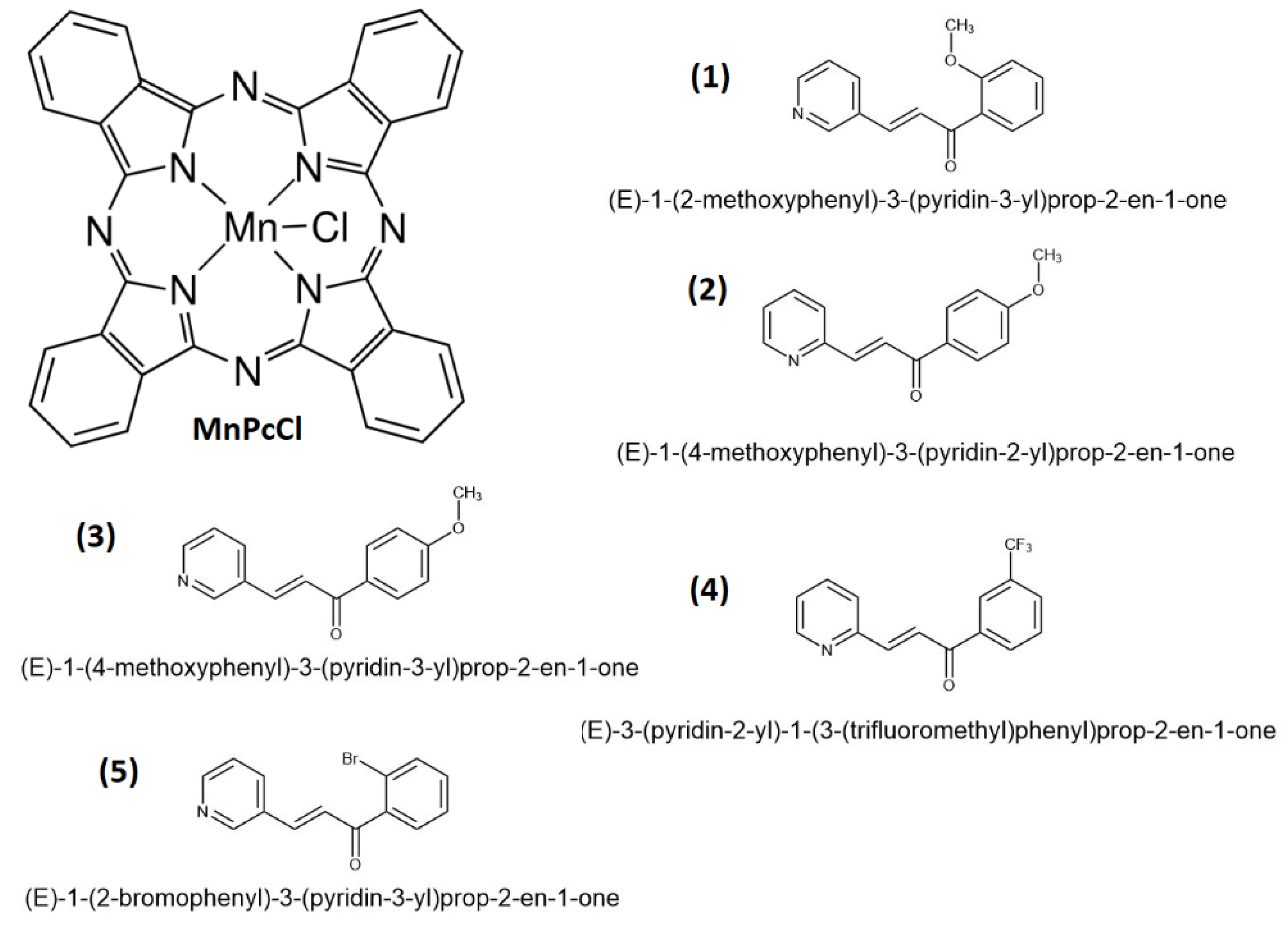
2.1. Doping of Organic Semiconductors (OSC)

All reagents and solvents were obtained from commercial sources and used without further purification (Sigma-Aldrich, Saint Louis, MO, USA). Chalcones were used in this study as organic dopants (see Figure 1), and their synthesis was carried out according to the procedure reported previously by some of the authors of this work [53]. Subsequently, manganese (III) phthalocyanine chloride, MnPcCl (C32H16ClMnN8) was chemically doped with chalcones by a simple reaction in absolute methanol in a conventionally heated Monowave 50 reactor with a pressure sensor (Anton Paar México, S.A. de C.V. Hidalgo, México). Afterward, 181 mg (0.3 mmol) of MnPcCl were added to 47.8 mg (0.2 mmol) of chalcone No. 1 (OS1), or 47.8 mg (0.2 mmol) of chalcone No. 2 (OS2), or 47.8 mg (0.2 mmol) of chalcone No. 3 (OS3), or 55.4 mg (0.2 mmol) of chalcone No. 4 (OS4), or 57.6 mg (0.2 mmol) of chalcone No. 5 (OS5), respectively and then dissolved in 6 mL of absolute methanol. The reactor was operated with a borosilicate glass vial and manually closed by a cover with an integrated pressure (0–20 bar) and temperature sensor. Every compound remained on reflux for 40 min using a 2-step method: ramp to temp for 10 min at 140 °C and hold time for 30 min at 140 °C, with a stirrer speed of 600 rpm and a cooling temperature of 30 °C. The doped semiconductors were then filtered, purified, and dried in a vacuum. These doped semiconductors are insoluble in organic solvents, such as ethanol, acetone, isopropanol, and methanol. In order to verify the purity of the doped semiconductors, thin plate chromatography was applied to all of them. Finally, to verify the main functional groups of the organic semiconductors, IR-spectroscopy analysis was performed on a Nicolet iS5-FT spectrometer (Thermo Fisher Scientific Inc., Waltham, MA, USA), using KBr pellets on a wavelength range of 4000 to 500 cm−1.

2.2. Thin Film Deposition and Characterization

Organic semiconductors OS1, OS2, OS3, OS4, and OS5 were subsequently deposited using the high-vacuum sublimation technique. The substrates were made from polyethylene terephthalate film, ITO coated (PET-ITO) monocrystalline n-type and p-type silicon wafers, and Corning glass. Except for the substrate PET-ITO, all other substrates were previously submitted to a sonication cleaning process with different solvents and were dried under a vacuum. The organic semiconductors were deposited by sublimation on a vacuum chamber (Intercovamex, S.A. de C.V., Cuernavaca, Morelos, Mexico). The vacuum was accomplished through two pumps: a mechanical pump that generated an initial pressure of 10−3 Torr and a turbo-molecular pump that generated the final deposition pressure of 10−6 Torr. The deposition process involved evaporation equipment with molybdenum and tantalum boats. During the deposition processes, the film thickness was evaluated with a high-resolution thickness monitor and a SISMONI-1C-3mHz quartz sensor (Intercovamex, S.A. de C.V., Cuernavaca, Morelos, Mexico). A further IR analysis was carried out in the film deposited on the n-type silicon wafers with a Nicolet iS5-FT (Thermo Fisher Scientific Inc., Waltham, MA, USA). A ZEISS EVO LS 10 scanning electron microscope (Zeiss International Inc., Göttingen, Germany) was used to analyze the thin films supported by the glass substrate. The films on glass substrates were also used to determine the optical absorption of the materials with a Unicam spectrophotometer, model UV300 (Thermo Fisher Scientific Inc., Waltham, MA, USA), in the wavelength range of 200–1100 nm. In order to estimate the charge-carrying properties of the doped semiconductors, a flexible device was manufactured. The doped semiconductor BHJ film was placed between the ITO (anode) and the conductive carbon paint (cathode). The thickness and area of the MnPcCl–chalcone BHJ were 76 nm and 4.61 cm2, respectively. Electric measurements were performed with a programmable voltage source, namely the Keithley 4200-SCS-PK1 auto-ranging pico-ammeter (Tektronix Inc., Beaverton, OR, USA). The evaluation of the electrical behavior of the devices was performed with the voltage source and a sensing station with a lighting- and temperature-controller circuit from Next Robotix (Comercializadora KMox, S.A. de C.V., Mexico City, Mexico).

3. Results and Discussion

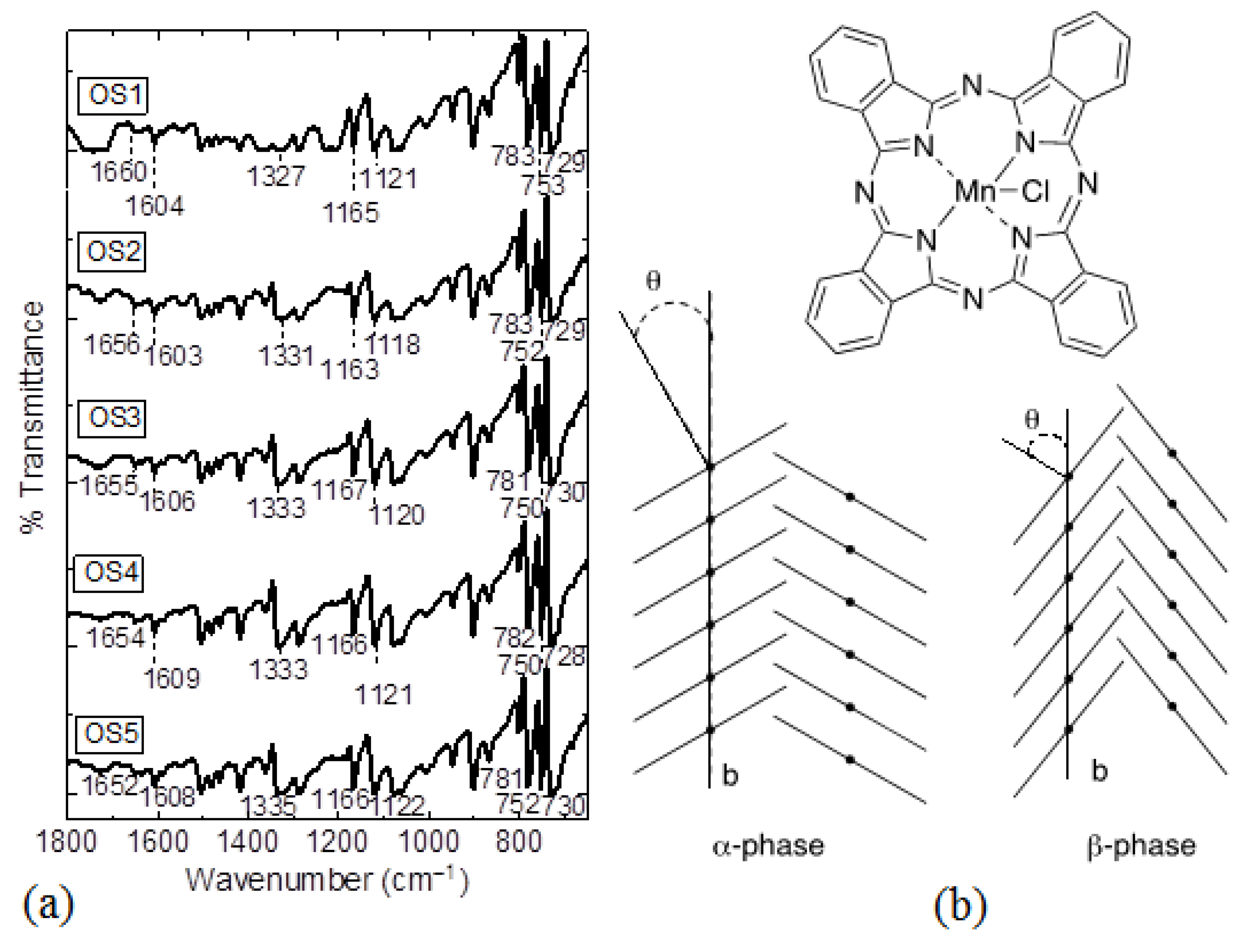
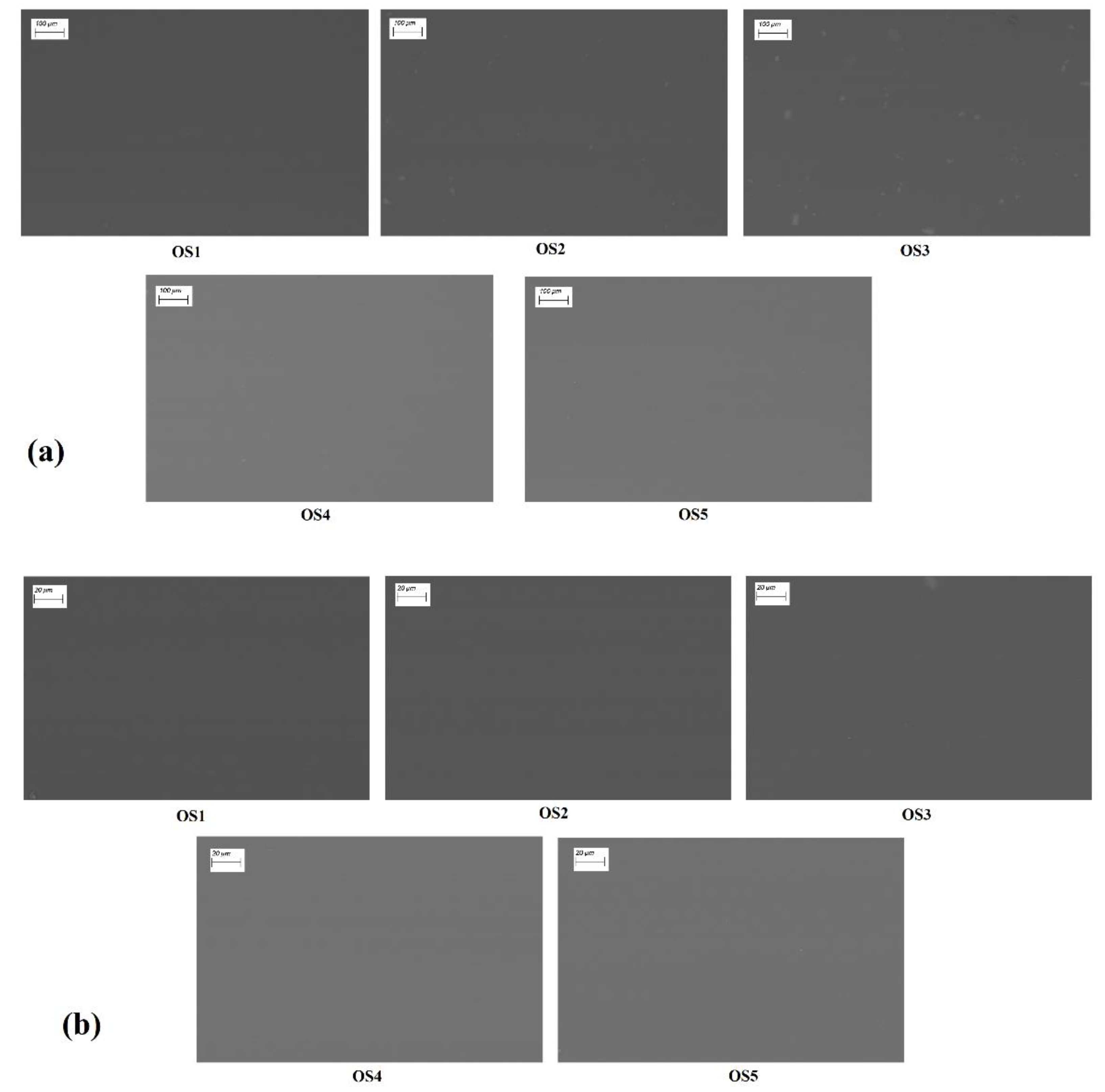
3.1. Doping, Deposition, and Characterization of the Semiconductor Films

The doping of MnPcCl with chalcone molecules was carried out as described in the experimental section. The IR spectra shown in Figure 2a were performed to verify the presence of the main functional groups in the doped MnPcCl–chalcone (OS1, OS2, OS3, OS4, and OS5) in KBr and, based on these results, determine the viability of depositing the thin films by means of the vacuum evaporation technique. Vacuum evaporation is a clean technique for thin film deposition, as a vacuum is applied to reduce contaminants such as oxygen and water and, on the other hand, to dope and create interpenetrating donor–acceptor networks [8]. However, the thermal gradients generated during the deposition can chemically break down the semiconductor molecules; hence, the importance of IR spectroscopy. The signals corresponding to both MnPcCl and chalcone in KBr pellets can be identified in Figure 2a. Regarding MnPcCl in the spectrum, the band responsible for the pyrrole in-plane stretch vibration in the phthalocyanine ring is observed around 1333 cm−1, and the bands located around 1166, 1119, and 753 cm–1 result from the interaction between carbon and hydrogen atoms [31,37,54]. The α-form in MnPcCl can be characterized by a band around 727 cm−1, while the β-form can be characterized by a band around 782 cm−1 [37,55]. The difference between the crystalline structures is the angle formed between the symmetry axis and the stacking direction (see Figure 2b). The α-form has an angle θ = 26.5° with this axis, while the β-form has an angle θ = 45.8° [37,55]. According to the IR spectra, MnPcCl in the doped materials has both crystalline forms. As for the chalcones used as dopants, the IR spectrum of Figure 2a shows the band corresponding to carbonyl at around 1669 cm−1; it is also possible to observe the signal corresponding to the double C=C bonds in the neighborhood of 1610 cm−1. After vacuum evaporation, IR spectroscopy was performed again, now on the MnPcCl–chalcone films deposited on n-type silicon. The results are shown in Table 1, in which the vibrational modes of the films are also compared with those obtained for these materials in KBr pellets. Both vibrational modes are similar, with a small difference due to film stress attributed to the deposition process. From the above, it is concluded that the MnPcCl–chalcone doped semiconductors did not suffer any degradation during the formation of the thin films.
The morphology of the films was studied at different magnifications through SEM; Figure 3 shows the microphotographs at 250× (Figure 3a) and 1250× (Figure 3b). The study at high magnifications was carried out with the purpose of looking for micrometric-sized imperfections in the films, which can affect charge transport and, in general, electrical behavior. The study at low magnifications, in addition to looking for imperfections in the films, helped to analyze their morphology on a larger surface. With both magnifications, practically the same morphologies are observed. The difference in the chalcone used as dopant apparently does not influence the quality of the deposit. Regardless of the dopant used, a homogeneous morphology formed by fine grains and a free surface without holes are observed. There seems to be only one phase, which is an indication of an adequately dispersed heterojunction in each of the films. At 250×, the particles that are observed on the surface of films OS2 and OS3 are a product of the deposition process and can be removed mechanically with the help of nitrogen flow. From the results obtained, one may observe that the quality of the films mainly depends on the operating parameters during their manufacture, which was similar for all the deposits. Vacuum evaporation is a technique that allows the formation of homogeneous MnPcCl–dopant films; this uniformity enhances their optical and electric properties.

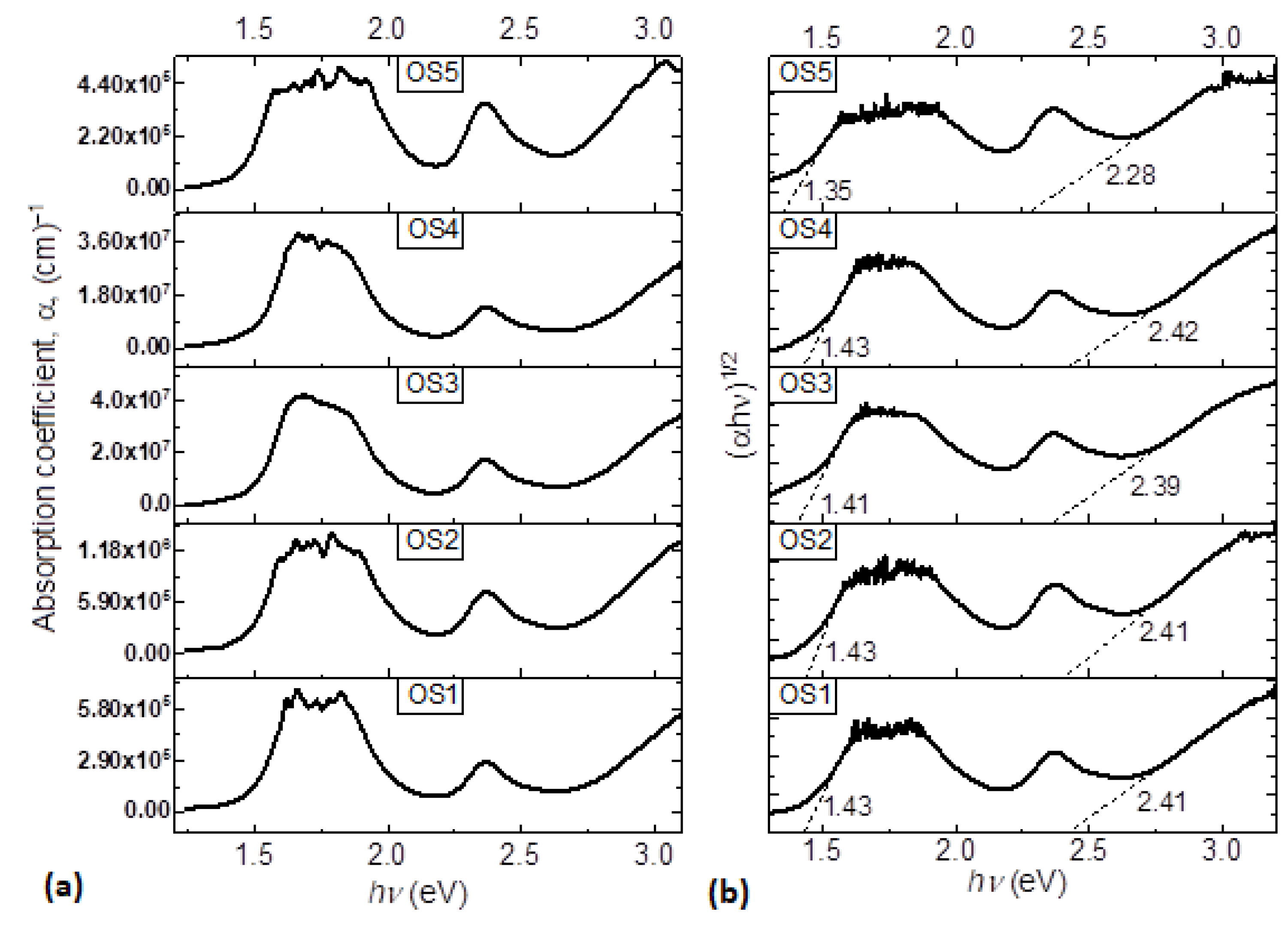
3.2. Optical Behavior Evaluation

The absorption of light by organic semiconductors gives an insight into their electronic transfer characteristics. For this reason, UV-vis spectroscopy was carried out in the precursors in solid-state form and in the MnPcCl–chalcone films deposited on Corning glass. According to the literature, the spectrum of the chalcones in Figure 4a shows the absorption peaks in the region between 290 and 397 nm [56,57]. Figure 4b shows the UV-vis spectra for the MnPcCl–chalcones films, which were strongly influenced by the presence of MnPcCl. Phthalocyanines are compounds with high optical stability that absorb radiation corresponding to the visible portion of the electromagnetic spectrum. The UV-vis spectrum of the MnPcCl in Figure 4a presents three absorption bands in the visible region: the Q band, a band related to charge transfer (CT), and the B band [13,36,58,59]. The Q band is associated with π–π* transitions from the Highest Occupied Molecular Orbital (HOMO) to the Lowest Unoccupied Molecular Orbital (LUMO) between orbitals of symmetry au and bg, respectively. According to the spectra shown in Figure 4b for the MnPcCl–chalcone films, this band is located between 630–800 nm and is responsible for the blue-green coloration of these materials. It is important to consider that the interval between 630 and 800 nm is characterized by a high absorption; the edge of photoabsorption corresponds mainly to the visible range of the spectrum, which is a relevant feature for photovoltaic systems [36]. On the other hand, the CT band is located between 465 and 570 nm and is associated with unsaturated manganese ions. Finally, the B band at region 280–460 nm is due to more energetic electronic transitions, related to π–π* transitions from occupied orbitals of symmetry bu and au at lower energies than the LUMO. It is important to consider that this band is also influenced by the chalcone used as a dopant [46,56,60]. The spectrum has maximum absorption in the region 360–390 nm, which corresponds to the π → π* transition for the chalcones [46,56,60]. Figure 4c shows the transmittance for the MnPcCl–chalcone films over Corning glass; the spectra show a peak at 470 nm, reaching a transmittance of 27% [36]. Two more peaks have been identified at 570 and around 925 nm for MnPcCl–chalcone films, suggesting potential applications for these films in photovoltaics, photodiodes, and photo sensors [36,61]. Finally, in the spectra of Figure 4, changes in film absorbance and transmittance can be observed. The structure of the chalcone acting as a dopant seems to cause these modifications. For example, the highest overall absorption and lowest transmission have corresponded to semiconductor film OS1, while the lowest absorption and highest transmission were observed in film OS3. It is interesting to notice that chalcones one and three have a similar structure (see Figure 1), as both have a pyridine in position three and are only distinguished by a position change of the methoxy group (–OCH3) in the aromatic ring. It seems that the position change of the –OCH3 group (from para- to ortho-) modifies the optical behavior, given that electronic delocalization in chalcone is affected by the presence of the carbonyl group as well as by the position of the –OCH3 group, which in the ortho- pattern may be interacting with the carbonyl by a hydrogen bond through the vinyl hydrogen α.
The absorption coefficients, α, for MnPcCl–chalcone films, as functions of wavelength, are shown in Figure 5a. In order to calculate α, the following expression is used:
α = ln ( T / d )
where d is the thickness of the films and T is their transmittance. It can be observed that α values are in the range of 105–107 cm−1 and are superior to those reported for pristine MnPcCl [27], as well as for other MPcs [26,62]. In this case, the value of α changes drastically, depending on the type of chalcone used as a dopant. Chalcones have remarkable linear and nonlinear optical properties [37,38,39,40,41,42,43] and, according to the results obtained by Maidur et al. [46,56], the presence of chalcones increases film absorption. On the other hand, most electronic transitions in organic semiconductors occur between the HOMO and the LUMO, with the bandgap representing the region between them. If α ≥ 10−4 cm−1, there is a general expression that relates α to the energy bandgap [63]. The energy dependence of α is given by Tauc’s relationship [36,62,63,64,65]:
( α h ν ) = A ( h ν E g )   r
Parameter A depends on the transition probability, Eg is the energy band gap, hν is the photon energy, and r is a number that characterizes the transition process and takes the value r = 2 for indirect transitions in amorphous films [66,67]. Figure 5b shows Tauc’s plots of the films, from which the Eg values could be calculated by extrapolating a tangent line to the hν axis. According to Figure 5b, the band gap values change slightly as a result of modifications in the chalcone structure. Figure 5b shows two energy band gaps: the optical band gap (Egopt) at low hν and the fundamental gap (Eg) at high hν [36]. The Egopt value corresponds to transitions from the HOMO to the LUMO level, and the Eg value results from transitions corresponding to the 3d → π* orbit energy bands [36,68]. Egoptvalues for the films were found between 1.35 and 1.43 eV, while the Eg values were located between 2.28 and 2.42 eV. The values of Egopt and Eg are within the range of band gaps reported in the literature and are also obtained by Tauc’s method for films based on MnPcCl [24,36,69]. It is important to mention as well that, in all cases, the band gap is also within the range accepted for organic semiconductors (whose limit is 3 eV). The low Egopt values obtained in this work suggest that films with MnPcCl–chalcone may be good candidates for use in optoelectronic devices, as Egopt defines the nature of the electroluminescent signal in light-emitting diodes and light absorption efficiency in solar cells. To provide further evidence in this regard, an evaluation of the electric behavior is relevant at this point.

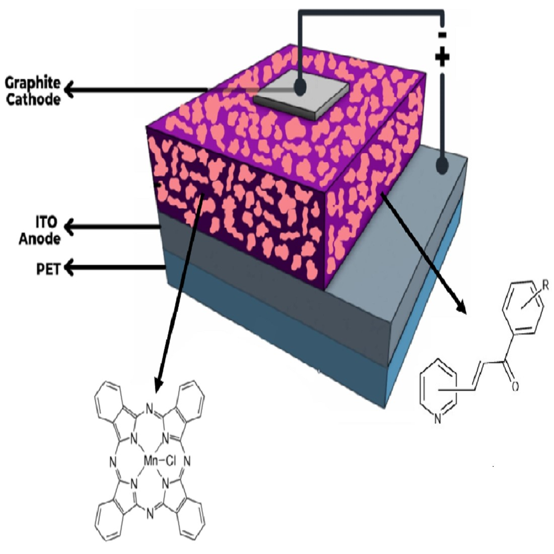
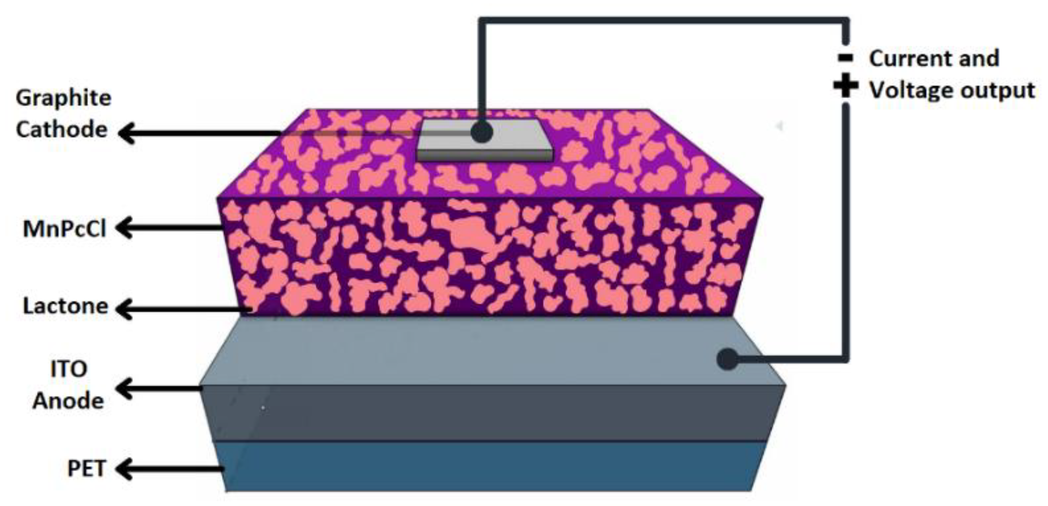
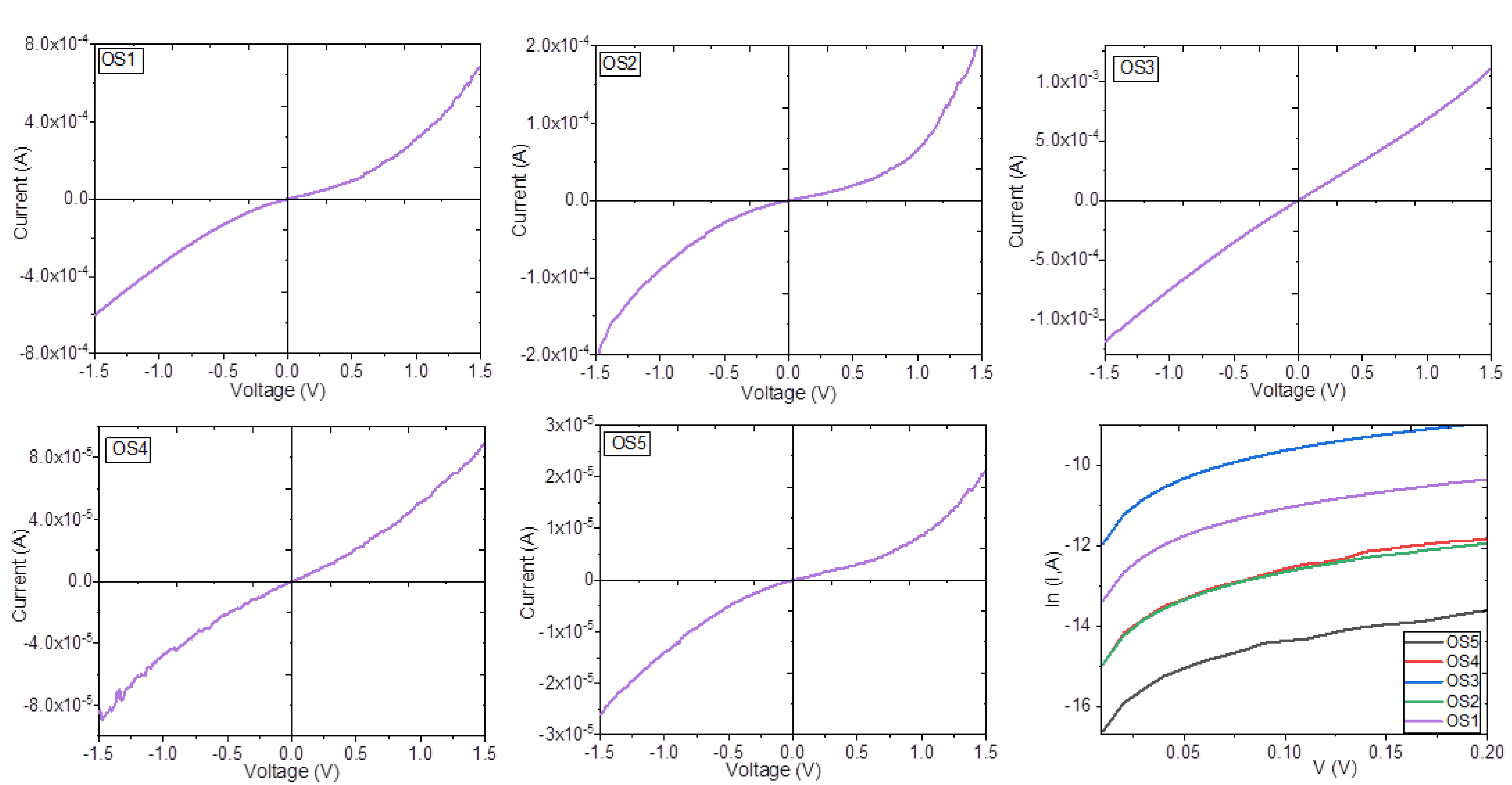
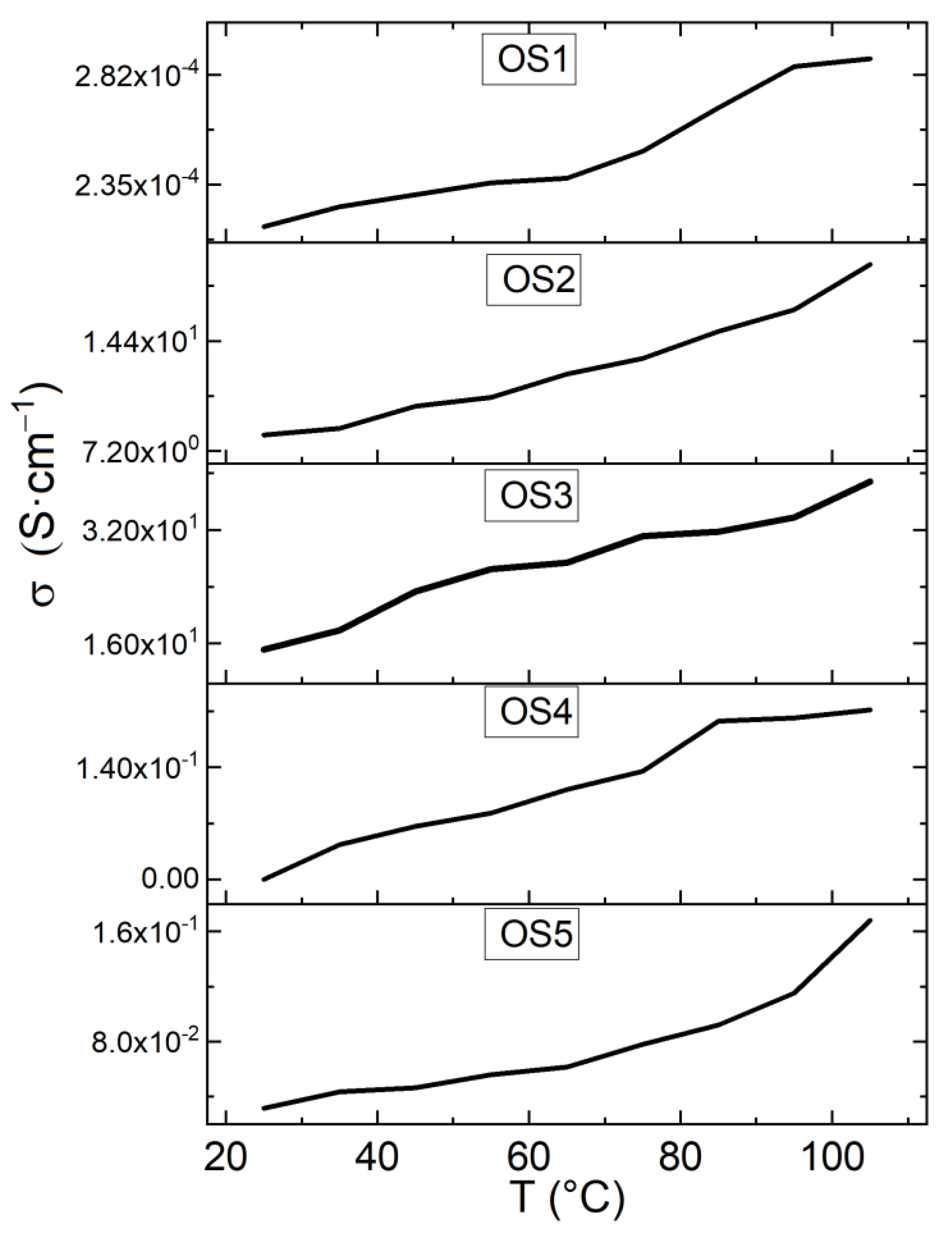
3.3. Manufacture of the Devices and Electrical Characterization

Flexible devices were manufactured in order to evaluate the electric behavior of the MnPcCl–chalcone films. A schematic diagram of the devices is shown in Figure 6. The active layer was constituted by MnPcCl–chalcone; thus, at any point within the film, there is a donor–acceptor mixture. The bulk heterojunction (BHJ) is intended to increase the interface area between the two species while reducing the distance between them, which promotes the excitonic dissociation processes and reduces the recombination processes [24,70,71]. The transparent substrate used in the manufacture of the device is made of PET, the anode is made of a transparent ITO conductor, and the cathode is made of graphite, also a conductor. The performance of the device is best illustrated by its current-voltage (I-V) characteristics. The forward- and reverse-bias I-V characteristics of the MnPcCl–chalcone BHJ films at room temperature are shown in Figure 7a–e. The highest current value was recorded in the device with the OS3 film, followed by OS1, OS2, OS4, and OS5. Such a result might be indicative of a more efficient charge injection from film OS3. This fact could be due to a lower injection barrier between such film and the electrode leading to efficient charge transport between MnPcCl and the chalcone three. Chalcones with a methoxy group donate electron density through the aromatic ring, so they may be considered partial electron donors. The presence of the methoxy group in OS1, OS2, and OS3 (see Figure 1), conversely, promotes a partial electron acceptor behavior in MnPcCl, facilitating charge transport in the BHJ film.
Additionally, from Figure 7, it is evident that the presence of chalcone significantly modifies the semiconductor’s behavior. The devices with films OS3 and OS4 show a quasi-ohmic behavior, which may allow their use as electrodes in optoelectronic devices; this dependence could be related to the injection of charges towards the semiconductor. On the other hand, there is no noticeable rectification at the I-V curve of the device with film OS2; the symmetrical behavior is related to the ambipolarity of the device, as film OS2 can transport both electrons and holes. For this semiconductor, one obtains Egopt < 1.8 eV so that it may be used in the manufacture of optoelectronic devices such as thin-layer organic transistors [54,72] or active-layer solar cells [3,8]. Finally, in the I-V curves for the devices with films OS1 and OS5, the existence of leakage current for OS1 and OS5 was observed [29]. This behavior is common in diode-type devices [73,74], although charge transport mechanisms should be studied in more detail. A semilogarithmic plot of the forward current vs. applied voltage for the same devices is shown in Figure 7. At applied voltages smaller than 0.002 V, the logarithm of the current increases linearly; this suggests that thermionic emission may be the dominant conduction mechanism in such a potential range [29,73]. The extrapolated intercept of the linear portion of the curves with the I-axis, at V = 0 V, yields the values of saturation current (Is), which are reported in Table 2 [73]. Nevertheless, since the linearity range occurs in a very small interval (0.01–0.02 V), the dominant conduction mechanism for voltages higher than 0.02 V is defined by space-charge-limited current (SCLC) [29,73,74]. Within the contact between the electrodes and the semiconductor film, in the vicinity of the electrodes, spatial charges are formed which oppose the flow of current through the semiconductor film. Beyond a certain threshold in the applied field, current saturation occurs.
Electrical conductivity (σ) is an important parameter; in semiconductor thin films, it increases with temperature. For each device, σ was evaluated at applied voltages of 0.1, 0.5, and 1.0 V and at different temperatures. Table 2 shows the values of σ at room temperature, while Figure 8 shows the temperature dependence of σ at 0.5 V within a temperature range of 25 to 100 °C. With respect to the results reported in Table 2, it is observed that, by increasing the voltage, an increase in the σ of the device occurs, with the OS5 device presenting the highest conductivity. However, σ values at room temperature for all devices are within the range for organic semiconductor materials (10−6 to 10−1 S·cm−1); this is important because an organic semiconductor is generally defined in terms of its conductivity at room temperature. These results are related to the chalcone presence and the features it contributes to the semiconductor: (i) a high electronic delocalization, permitting charge transport; (ii) an increase in the BHJ contact surface, which improves excitonic diffusion between MnPcCl and the chalcone, and (iii) a BHJ-generated anisotropy, producing conduction channels for charge transport. For the results in Figure 8, in all the devices, conductivity increases with temperature, as expected for semiconductors. Within the range, conductivity increases by two orders of magnitude in OS4 and less than an order of magnitude in OS1, OS2, OS3, and OS5. These results supplement earlier studies regarding the use of MnPcCl–chalcone semiconducting films for optoelectronic applications.

4. Conclusions

Organic semiconductors of MnPcCl and chalcones as dopants were prepared. Thin films of these semiconductors were deposited by high vacuum thermal evaporation, which is a technique that allows film deposition of high purity and uniform morphology. According to the IR spectroscopic results, the MnPcCl–chalcone organic semiconductors do not undergo degradation during the deposition process. MnPcCl–chalcone films showed the Q band between 630–800 nm, a band due to charge transfer in the region between 465 and 570 nm, and the B band at region 280–460 nm. The films present two energy gaps: the optical band around 1.40 eV and the fundamental gap around 2.35 eV. Electrical conductivity at room temperature varies from 1.8 × 10⁻⁵ to 1.5 × 101 S·cm−1 and increases with temperature. Optoelectronic behavior and properties of the MnPcCl–chalcone films are completely determined by the structure and type of chalcone, with the best properties arising in chalcones that have a methoxy group as a substituent. Thus, MnPcCl–chalcone doped semiconductors show promise, in terms of optical and electrical properties, for possible use in electronic devices.

Author Contributions

Conceptualization, M.E.S.V., M.J.C.J., G.C.R. and C.Á.T.; methodology, M.J.C.J., G.C.R., R.B.I. and M.E.S.V.; software M.E.S.V., M.J.C.J. and R.B.I.; validation, M.E.S.V., G.C.R., R.B.I., J.R.Á.B. and C.Á.T.; formal analysis, M.E.S.V., M.J.C.J., J.R.Á.B., R.B.I. and C.Á.T.; research, M.E.S.V., M.J.C.J., C.Á.T. and J.R.Á.B.; resources, M.E.S.V.; data curation, M.E.S.V. and R.B.I.; writing-original draft preparation, M.E.S.V., M.J.C.J., G.C.R., R.B.I. and C.Á.T.; writing—review and editing, M.E.S.V., R.B.I., J.R.Á.B. and C.Á.T.; visualization, M.E.S.V. and J.R.Á.B.; supervision, M.E.S.V. and C.Á.T.; project administration, M.E.S.V. and C.Á.T.; funding acquisition, M.E.S.V. and C.Á.T. All authors have read and agreed to the published version of the manuscript.

Funding

M.E. Sánchez Vergara acknowledges the financial support from Universidad Anáhuac México, Project number NNAIASEVM16070616. C. Álvarez Toledano gratefully acknowledges the financial support of the DGAPA-PAPIIT Projet number IN203120.

Institutional Review Board Statement

Not applicable.

Informed Consent Statement

Not applicable.

Conflicts of Interest

The authors declare no conflict of interest.

References

  1. Shoaee, S.; Sanna, A.L.; Sforazzini, G. Elucidating charge generation in green-solvent processed organic solar cells. Molecules 2021, 26, 7439. [Google Scholar] [CrossRef]
  2. Moore, K.; Wei, W. Applications of carbon nanomaterials in perovskite solar cells for solar energy conversion. NMS 2021, 3, 276–290. [Google Scholar] [CrossRef]
  3. Husain, A.A.F.; Hasan, W.Z.W.; Shafie, S.; Hamidon, M.S.; Pandey, S.S. A review of transparent solar photovoltaic technologies. Renew. Sust. Energ. Rev. 2018, 94, 779–791. [Google Scholar] [CrossRef]
  4. Green, M.; Dunlop, E.; Hohl-Ebinger, J.; Yoshita, M.; Kopidakis, N.; Hao, X. Solar cell efficiency tables (version 57). Prog. Photovolt. Res. Appl. 2021, 29, 3–15. [Google Scholar] [CrossRef]
  5. Liu, Q.; Jiang, Y.; Jin, K.; Qin, J.; Xu, J.; Li, W.; Xiong, J.; Liu, J.; Xiao, Z.; Sun, K.; et al. 18% Efficiency organic solar cells. Sci. Bull. 2020, 65, 272–275. [Google Scholar] [CrossRef] [Green Version]
  6. Wu, J.; Gao, M.; Chai, Y.; Liu, P.; Zhang, B.; Liu, J.; Ye, L. Towards a bright future: The versatile applications of organic solar cells. MRE 2021, 1, 100062. [Google Scholar] [CrossRef]
  7. Shi, D.; Guo, Z.; Bedford, N. 10-Nanoenergy materials. MNT 2015, 1, 255–291. [Google Scholar] [CrossRef]
  8. Günes, S.; Neugebauer, H.; Sariciftci, N.S. Conjugated polymer-based organic solar cells. Chem. Rev. 2007, 107, 1324–1338. [Google Scholar] [CrossRef]
  9. Gorduk, S.; Altindal, A. Peripherally tetra-substituted metallophthalocyanines bearing carboxylic acid groups for efficient dye sensitized solar cells. J. Mol. Struct. 2019, 1196, 747–753. [Google Scholar] [CrossRef]
  10. Sukhikh, A.; Bonegardt, D.; Klyamer, D.; Krasnov, P.; Basova, T. Chlorosubstituted Copper phthalocyanines: Spectral study and structure of thin films. Molecules 2020, 25, 1620. [Google Scholar] [CrossRef] [Green Version]
  11. Madhuri, K.P.; Sagade, A.A.; Santra, P.K.; John, N.S. Templating effect of single-layer graphene supported by an insulating substrate on the molecular orientation of lead phthalocyanine. Beilstein J. Nanotechnol. 2020, 11, 814–820. [Google Scholar] [CrossRef] [PubMed]
  12. Zanotti, G.; Angelini, N.; Mattioli, G.; Paoletti, A.M.; Pennesi, G.; Caschera, D.; Sobolev, A.P.; Beverina, L.; Calascibetta, A.M.; Sanzone, A.; et al. [1]Benzothieno[3,2-b][1]benzothiophene-phthalocyanine derivatives: A subclass of solution-processable electron-rich hole transport materials. ChemPlusChem 2020, 85, 1–12. [Google Scholar] [CrossRef] [PubMed]
  13. Cranston, R.R.; Lessard, B.H. Metal phthalocyanines: Thin-film formation, microstructure, and physical properties. RSC Adv. 2021, 11, 21716–21737. [Google Scholar] [CrossRef]
  14. Williams, G.; Sutty, S.; Klenkler, R.; Aziz, H. Renewed interest in metal phthalocyanine donors for small molecule organic solar cells. Sol. Energy Mater. Sol. Cells. 2014, 124, 217–226. [Google Scholar] [CrossRef]
  15. Grant, T.M.; Josey, D.S.; Sampson, K.L.; Mudigonda, T.; Bender, T.P.; Lessard, B.H. Boron subphthalocyanines and silicon phthalocyanines for use as active materials in organic photovoltaics. Chem. Rec. 2019, 19, 1093–1112. [Google Scholar] [CrossRef]
  16. Reddy, G.; Devulapally, K.; Islavath, N.; Giribabu, L. Metallated macrocyclic derivatives as a hole—Transporting materials for perovskite solar cells. Chem Rec. 2019, 19, 2157–2177. [Google Scholar] [CrossRef]
  17. Urbani, M.; de la Torre, G.; Nazeeruddin, M.K.; Torres, T. Phthalocyanines and porphyrinoid analogues as hole- and electron-transporting materials for perovskite solar cells. Chem. Soc. Rev. 2019, 48, 2738–2766. [Google Scholar] [CrossRef]
  18. Yu, Z.; Hagfeldt, A.; Sun, L. The application of transition metal complexes in hole-transporting layers for perovskite solar cells: Recent progress and future perspectives. Coord. Chem. Rev. 2020, 406, 213143. [Google Scholar] [CrossRef]
  19. Ranta, J.; Kaunisto, K.; Niskanen, M.; Efimov, A.; Hukka, T.I.; Lemmetyinen, H. Monoisomeric phthalocyanines and phthalocyanine−Fullerene dyads with polar side chains: Synthesis, modeling, and photovoltage. J. Phys. Chem. 2014, 118, 2754–2765. [Google Scholar] [CrossRef]
  20. Martínez-Díaz, M.V.; de la Torre, G.; Torres, T. Lightning porphyrins and phthalocyanines for molecular photovoltaics. Chem. Commun. 2010, 46, 7090–7108. [Google Scholar] [CrossRef]
  21. de la Torre, G.; Claessens, C.G.; Torres, T. Phthalocyanines: Old dyes, new materials. Putting color in nanotechnology. Chem. Commun. 2007, 2000–2015. [Google Scholar] [CrossRef] [PubMed]
  22. Mack, J.; Kobayashi, N. Low symmetry phthlocyanines and their analogues. Chem. Rev. 2011, 111, 281–321. [Google Scholar] [CrossRef] [PubMed]
  23. Martínez-Díaz, M.V.; Ince, M.; Torres, T. Phthalocyanines: Colorful macroheterocyclic sensitizers for dye-sensitized solar cells. Monatsh. Chem. 2011, 142, 699–707. [Google Scholar] [CrossRef]
  24. El-Zaidia, E.F.M. Studies structure, surface morphology, linear and nonlinear optical properties of nanocrystalline thin films of manganese (III) phthalocyanine chloride for photodetectors application. Sens. Actuator 2021, 330, 112828. [Google Scholar] [CrossRef]
  25. Grobosch, M.; Mahns, B.; Loose, C.; Friedrich, R.; Schmidt, C.; Kortus, J.; Knupfer, M. Identification of the electronic states of manganese phthalocyanine close to the Fermi level. Chem. Phys. Lett. 2011, 505, 122–125. [Google Scholar] [CrossRef]
  26. El-Nahass, M.M.; Soliman, H.S.; Khalifa, B.A.; Soliman, I.M. Structural and optical properties of nanocrystalline aluminum phthalocyanine chloride thin films. Mater. Sci. Semicond. Process. 2015, 38, 177–183. [Google Scholar] [CrossRef]
  27. El-Zaidia, E.F.M.; Qashou, S.I.; Darwish, A.A.A.; Yahia, I.S. Thermally evaporated of homogeneous nanostructured gallium-phthalocyanine-chloride films: Optical spectroscopy. Opt. Mater. 2020, 109, 110407. [Google Scholar] [CrossRef]
  28. Darwish, A.A.A.; Hamdalla, T.A.; El-Zaidia, E.F.M.; Hanafy, T.A.; Issa, S.A.M.; Yahia, I.S. Thin films of nanostructured gallium (III) chloride phthalocyanine deposited on FTO: Structural characterization, optical properties, and laser optical limiting. Phys. B Condens. Matter. 2020, 593, 412321. [Google Scholar] [CrossRef]
  29. Zeyada, H.M.; El-Nahass, M.M.; El-Menyawy, E.M.; El-Sawah, A.S. Electrical and photovoltaic characteristics of indium phthalocyanine chloride/p-Si solar cell. Synth. Met. 2015, 207, 46–53. [Google Scholar] [CrossRef]
  30. Soliman, I.M.; El-Nahass, M.M.; Khalifa, B.A. Characterization and photovoltaic performance of organic device based on AlPcCl/p-Si heterojunction. Synth. Met. 2015, 209, 55–59. [Google Scholar] [CrossRef]
  31. Touka, N.; Benelmadjat, H.; Boudine, B.; Halimi, O.; Sebais, M. Copper phthalocyanine nanocrystals embedded into polymer host: Preparation and structural characterization. J. Assoc. Arab Univ. Basic Appl. Sci. 2013, 13, 52–56. [Google Scholar] [CrossRef]
  32. Chau, L.K.; England, C.D.; Chen, S.; Armstrong, N.R. Visible absorption and photocurrent spectra of epitaxially deposited phthalocyanine thin films: Interpretation of exciton coupling effects. J. Phys. Chem. 1993, 97, 2699–2706. [Google Scholar] [CrossRef]
  33. Sánchez-Vergara, M.E.; Rivera, M. Investigation of optical properties of annealed aluminum phthalocyanine derivatives thin films. J. Phys. Chem. Solids 2014, 75, 599–605. [Google Scholar] [CrossRef]
  34. Soliman, I.M.; El-Nahass, M.M.; Mansour, Y. Electrical, dielectric and electrochemical measurements of bulk aluminum phthalocyanine chloride (AlPcCl). Solid State Commun. 2016, 225, 17–21. [Google Scholar] [CrossRef]
  35. Rivera, M.; Reyes, B.; Sánchez-Vergara, M.E.; Mendoza-Huizar, L.H. Conductive Behavior and Morphology of Axially Modified Gallium Phthalocyanine Thin Films onto Indium Tin Oxide Substrates. AMPC 2016, 6, 211–219. [Google Scholar] [CrossRef] [Green Version]
  36. Darwish, A.A.A.; Helali, S.; Qashou, S.I.; Yahia, I.S.; El-Zaidia, E.F.M. Studying the surface morphology, linear and nonlinear optical properties of manganese (III) phthalocyanine chloride/FTO films. Phys. B Condens. Matter. 2021, 622, 413355. [Google Scholar] [CrossRef]
  37. Custodio, J.M.F.; Vaz, W.F.; Faria, E.C.M.; Anjos, M.M.; Campos, C.E.M.; Oliveira, G.R.; Martins, F.T.; da Silva, C.; Valverde, C.; Osório, F.A.P.; et al. On the potential as nonlinear optical material of a new chalcone derivative and its crystal and topological analysis. J. Mol. Struct. 2020, 1201, 127131. [Google Scholar] [CrossRef]
  38. Ali, M.K.M.; Elzupir, A.O.; Ibrahem, M.A.; Suliman, I.I.; Modwi, A.; Idriss, H.; Ibnaouf, K.H. Characterization of optical and morphological properties of chalcone thin films for optoelectronics applications. Optik 2017, 145, 529–533. [Google Scholar] [CrossRef]
  39. Vaz, W.; Custodio, J.; Silveira, R.; Castro, A.; Campos, C.; Anjos, M.; Oliveira, G.; Valverde, C.; Baseia, B.; Napolitano, H. Synthesis, Characterization, and third-order nonlinear optical properties of a new neolignane analogue. R. Soc. Chem. 2016, 6, 79215–79227. [Google Scholar] [CrossRef]
  40. Sai Kiran, M.; Anand, B.; Siva Sankara Sai, S.; Nageswara Rao, G. Second- and third-order nonlinear optical properties of bis-chalcone derivatives. J. Photochem. Photobiol. A Chem. 2014, 290, 38–42. [Google Scholar] [CrossRef]
  41. Abegão, L.M.G.; Fonseca, R.D.; Santos, F.A.; Souza, G.B.; Barreiros, A.L.B.S.; Barreiros, M.L.; Alencar, M.A.R.C.; Mendonça, C.R.; Silva, D.L.; De Boni, L.; et al. Second- and third-order nonlinear optical properties of unsubstituted and mono-substituted chalcones. Chem. Phys. Lett. 2016, 648, 91–96. [Google Scholar] [CrossRef]
  42. Krawczyk, P.; Pietrzak, M.; Janek, T.; Jędrzejewska, B.; Cysewski, P. Spectroscopic and nonlinear optical properties of new chalcone fluorescent probes for bioimaging applications: A theoretical and experimental study. J. Mol. Model. 2016, 22, 125. [Google Scholar] [CrossRef] [PubMed]
  43. Sarojini, B.; Narayana, B.; Ashalatha, B.; Indira, J.; Lobo, K. Synthesis, crystal growth and studies on non-linear optical property of new chalcones. J. Cryst. Growth. 2006, 295, 54–59. [Google Scholar] [CrossRef]
  44. Gasull, E.; Blanco, S.; Ferretti, F. A theoretical and experimental study of adsorption from dilute cyclohexane solutions of non-electrolytes: 4-X-chalcones on silica gel. J. Mol. Struct. Teochem. 2002, 579, 121–137. [Google Scholar] [CrossRef]
  45. Gu, C.L.; Liu, L.; Sui, Y.; Zhao, J.L.; Wang, D.; Chen, Y.J. Highly enantioselective Michael additions of α-cyanoacetate with chalcones catalyzed by bifunctional cinchona-derived thioureaorganocatalyst. Tetrahedron Asymmetry 2007, 18, 455–463. [Google Scholar] [CrossRef]
  46. Maidur, S.R.; Patil, P.S. Z-scan studies of third-order nonlinear optical and optical limiting properties of chalcones doped Poly(methyl methacrylate) thin films for visible laser protection. Opt. Mater. 2018, 84, 28–37. [Google Scholar] [CrossRef]
  47. Vidyashree, H.; Bhajantri, R.F.; Jagadish, N.; Sunil, G.R. Thiazole yellow G dyed PVA films for optoelectronics: Microstructural, thermal and photophysical studies. Mater. Res. Express 2016, 3, 075301. [Google Scholar] [CrossRef]
  48. Sweeting, S.G.; Hall, C.L.; Potticary, J.; Pridmore, N.E.; Warren, S.D.; Cremeens, M.E.; D´Ambruoso, G.D.; Matsumoto, M.; Hall, S.R. The solubility and stability of heterocyclic chalcones compared with trans-chalcones. Acta Cryst. 2020, B76, 13–17. [Google Scholar] [CrossRef] [Green Version]
  49. Asiri, A.M.; Khan, S.A. Synthesis, characterization and optical properties of mono-and bischalcone. Mater. Lett. 2011, 65, 1749–1752. [Google Scholar] [CrossRef]
  50. Janardhana, K.; Ravindrachary, V.; Kumar, P.R. Third order nonlinear optical studies of 1-(4- chloro phenyl)-3-(4-dimethylamino phenyl) prop-2-en-1-one. J. Cryst. Growth. 2013, 368, 11–20. [Google Scholar] [CrossRef]
  51. Devi, J.M.; Tharmaraj, J.; Ramakrishnan, S.; Ramachandran, K. On the thermal properties of metal (II) complexes of chalcone. Mater. Lett. 2008, 62, 852–856. [Google Scholar] [CrossRef]
  52. Praveen, A.; Jayarama, A. Crucial role of molecular planarity on the second order nonlinear optical property of pyridine based chalcone single crystals. J. Mol. Struct. 2015, 1088, 85–94. [Google Scholar] [CrossRef]
  53. Carmona-Reyes, G.; Ballinas-Indili, R.; Sánchez-Vergara, M.E.; Toscano, R.A.; Álvarez-Toledano, C. Regiodivergent synthesis of vinyl trifluoromethansulfonates c/d lactones: Via 1,6 addition/intramolecular one-pot annulation of 1,4-dihidropyridines derivated from pyridinyl propenones. Tetrahedron Lett. 2022, 88, 153591. [Google Scholar] [CrossRef]
  54. El-Nahass, M.M.; Abd-El-Rahman, K.F.; Al-Ghamdi, A.A.; Asiri, A.M. Optical properties of thermally evaporated tin-phthalocyanine dichloride thin films, SnPcCl2. Phys. B Condens. Matter. 2014, 344, 398–406. [Google Scholar] [CrossRef]
  55. Hart, M.M. Cationic Exchange Reactions Involving Dilithium Phthalocyanine. Master’s Thesis, Wright State University, Dayton, OH, USA, 2009. [Google Scholar]
  56. Maidur, S.R.; Patil, P.S. Linear optical and third-order nonlinear optical properties of anthracene chalcone derivatives doped PMMA thin films. Optik 2019, 190, 54–67. [Google Scholar] [CrossRef]
  57. Sun, J.; Wang, G.; Liu, C.; Shi, Y.; Zhao, M. Synthesis of four pyrene-containing chalcone derivatives: Achieving excellent third-order nonlinear optical properties by optimizing halopyridines. Opt. Laser Technol. 2019, 109, 600–607. [Google Scholar] [CrossRef]
  58. El-Nahass, M.M.; Farag, A.M.; Abd El-Rahman, K.F.; Darwish, A.A.A. Dispersion studies and electronic transitions in nickel phthalocyanine thin films. Opt. Laser Technol. 2005, 37, 513–523. [Google Scholar] [CrossRef]
  59. Özçeșmeci, M.; Nar, I.; Hamuryudan, E. Synthesis and electrochemical and spectroelectrochemical characterization of chloromanganese(III) phthalocyanines. Turk. J. Chem. 2014, 38, 1064–1072. [Google Scholar] [CrossRef]
  60. Maidur, S.R.; Jahagirdar, J.R.; Patil, P.S.; Chia, T.S.; Quah, C.K. Structural characterizations, Hirshfeld surface analyses, and third-order nonlinear optical properties of two novel chalcone derivatives. Opt. Mater. 2018, 75, 580–594. [Google Scholar] [CrossRef]
  61. Lu, M.; Wang, K.; Han, Y.; Yao, Y.; Gao, P.; Huang, C.; Zhang, W.; Xu, F. Synthesis, structure, and optical properties of manganese phthalocyanine thin films and nanostructures. Prog. Nat. Sci. Mater. Int. 2017, 27, 329–332. [Google Scholar] [CrossRef]
  62. Mahmoud, A.Z.; Darwish, A.A.A.; Qashou, S.I. Film thickness effects on nanorods organic films of azo quinoline derivatives for optical applications. Prog. Nat. Sci. Mater. Int. 2019, 29, 402–409. [Google Scholar] [CrossRef]
  63. Elesh, E.; Mohammed, Z. Morphological, linear and nonlinear properties of gallium phthalocyanine chloride annealed thin films. Optik 2020, 219, 165176. [Google Scholar] [CrossRef]
  64. El-Nahass, M.M.; El-Deeb, A.F.; Metwally, H.S.; Hassanien, A.M. Influence of annealing on the optical properties of 5,10,15,20-tetraphenyl-21H, 23H-porphine iron (III) chloride thin films. Mater. Chem. Phys. 2011, 125, 247–251. [Google Scholar] [CrossRef]
  65. Bardeen, J.; Blatt, F.J.; Hall, L.H. Energy Dependence of Indirect Optical Absorption in Semiconductors. In Proceedings of the Conference on Photoconductivity; Atlantic: Boston, MA, USA, 4–6 November 1965; p. 149. [Google Scholar]
  66. Dongol, M.; El-Nahass, M.; El-Denglawey, A.; Elhady, A.; Abuelwafa, A. Optical Properties of Nano 5,10,15,20-Tetraphenyl-21H,23H-Prophyrin Nickel (II) Thin Films. Curr. Appl. Phys. 2012, 12, 1178–1184. [Google Scholar] [CrossRef]
  67. Alghamdi, S.A.; Darwish, A.A.A.; Yahia, I.S.; El-Zaidia, E.F.M. Structural characterization and optical properties of nanostructured indium (III) phthalocyanine chloride/FTO thin films for photoelectric applications. Optik 2021, 239, 166780. [Google Scholar] [CrossRef]
  68. Alharbi, S.R.; Darwish, A.A.A.; Al Garni, S.E.; El Saeedy, H.I.; Abd El-Rahman, K.F. Influence of thickness and annealing on linear and nonlinear optical properties of manganese (III) chloride tetraphenyl porphine (MnTPPCl) organic thin films. Infrared Phys. Technol. 2016, 78, 77–83. [Google Scholar] [CrossRef]
  69. Van Duren, J.; Yang, X.N.; Loos, J.; Bulle-Liewma, C.W.T.; Sieval, A.B.; Hummelen, J.C.; Janssen, R.A.J. Relating the Morphology of Poly(p-phenylene vinylene)/Methanofullerene Blends to Solar-Cell Performance. Adv. Mater. 2004, 14, 425. [Google Scholar] [CrossRef]
  70. Reyes-Reyes, M.; Kim, K.; Carroll, D.L. High-efficiency photovoltaic devices based on annealed poly(3-hexylthiophene) and 1-(3-methoxycarbonyl)-propyl-1- phenyl-(6,6)C61(6,6)C61 blends. Appl. Phys. Lett. 2005, 87, 083506. [Google Scholar] [CrossRef]
  71. Peet, J.; Kim, J.Y.; Coates, N.E.; Ma, W.L.; Moses, D.; Heeger, A.J.; Bazán, G.C. Efficiency enhancement in low-bandgap polymer solar cells by processing with alkane dithiols. Nat. Mater. 2007, 6, 497. [Google Scholar] [CrossRef]
  72. Meijer, E.J.; de Leeuw, D.M.; Setayesh, S.; van Veenendaal, E.; Huisman, B.H.; Blom, P.W.M.; Hummelen, J.C.; Scherf, U.; Klapwijk, T.M. Solution-processed ambipolar organic field-effect transistors and inverters. Nat. Mater. 2003, 2, 678. [Google Scholar] [CrossRef]
  73. Shafai, T.S.; Anthopoulous, T.D. Junction properties of nickel phthalocyanine thin film devices utilizing indium injecting electrodes. Thin Solid Film. 2001, 398–399, 361–367. [Google Scholar] [CrossRef]
  74. Ahmad, Z.; Sayyad, M.H.; Karimov, K.S. CuPc based organic-inorganic hetero-junction with Au electrodes. J. Semicond. 2010, 31, 074002-1-4. [Google Scholar] [CrossRef]
Figure 1. Structure of MnPcCl and chalcones.
Coatings 12 00246 g001
Figure 2. (a) IR spectra of doped semiconductors in KBr pellets. (b) Structure of α and β-form for MnPcCl.
Coatings 12 00246 g002
Figure 3. SEM micrographs of MnPcCl–chalcone films at (a) 250× and (b) 1250×.
Coatings 12 00246 g003
Figure 4. (a) Absorbance of MnPcCl and chalcones 1–5. (b) Absorbance and (c) transmittance optical spectra of MnPcCl–chalcone films.
Coatings 12 00246 g004
Figure 5. (a) Absorption coefficients, α, and (b) plots of (αhν)1/2 versus photon energy (hν) of the MnPcCl–chalcone films.
Coatings 12 00246 g005
Figure 6. Cross section of the device.
Coatings 12 00246 g006
Figure 7. Current-Voltage (I-V) characteristic curves of the devices with OS films.
Coatings 12 00246 g007
Figure 8. Electric conductivity (σ) vs. T of the devices with OS films.
Coatings 12 00246 g008
Table 1. Band positions and assignments of MnPcCl–chalcone semiconductors in KBr pellets (powder) and films.
AssignmentPowder
(cm−1)
Film
(cm−1)
Powder
(cm−1)
Film
(cm−1)
Powder
(cm−1)
Film
(cm−1)
Powder
(cm−1)
Film
(cm−1)
Powder
(cm−1)
Film
(cm−1)
SampleOS1OS1OS2OS2OS3OS3OS4OS4OS5OS5
In-plane pyrrole stretching1327133513351333133213321334133113321333
C-H bending1164, 11191161, 11191167, 11191167, 11211167, 11191165, 11211166, 11201165, 11191166, 11191167, 1119
In-plane C-H deformation753752753752753754753754752754
α-form in MnPc729726724726729727729726727724
β-form in MnPc783782782779782780782778782778
C=O stretching bands of carbonyl1660166216561665165616621652166816521667
C=C bending of chalcone1607160416091609160716081607160716071603
Table 2. Electrical parameters of the devices with OS films.
DeviceIS (A)σ at 0.1 V
(S·cm−1)
σ at 0.5 V
(S·cm−1)
σ at 1.0 V
(S·cm−1)
OS12.24 × 10−82.92 × 10−23.16 × 10−25.56 × 10⁻²
OS22.32 × 10−81.55 × 10−51.89 × 10−52.82 × 10⁻⁵
OS31.18 × 10−71.43 × 10+11.51 × 10+13.02 × 10+1
OS42.73 × 10−96.27 × 10+08.26 × 10+01.45 × 10+1
OS57.14 × 10−107.64 × 10−17.64 × 10−17.73 × 10⁻¹
Publisher’s Note: MDPI stays neutral with regard to jurisdictional claims in published maps and institutional affiliations.

