1. Introduction
Metal ion irradiation combining HIPIMS discharges and pulsed bias synchronization has been demonstrated in recent years to be a powerful method to achieve an accurate management on film nanostructure and phase control for the deposition of transition metal (TM) nitrides [
1]. It allows the deposition of films with optimum mechanical properties as well as reduced accumulated stress compared to films deposited with gas-ion bombardment typical for direct current magnetron sputtering (DCMS). The selective attraction of metal ions at the substrate position optimizes the metal ion energy and momentum required during film growth. The target to substrate distance determines the time delay between the magnetron and bias voltage pulses which is primarily investigated by mass spectroscopy. In general, this method has been demonstrated for static configurations, i.e., the target to substrate separation remains constant once the optimum time delay has been selected [
2].
In this work, this concept of selective metal ion irradiation is extended by combining bipolar HIPIMS with conventional DC magnetron sputtering operation and DC biasing. The concept of bipolar HIPIMS was introduced some years ago by different groups and consists of applying a positive pulse with controlled pulse width and amplitude voltage after the conventional HIPIMS negative pulse [
3,
4]. This positive pulse allows the controlled acceleration of the positive ions (both metal and gas, but predominantly metal ions at the end of the HIPIMS pulse [
5]) towards the substrate, thus, promoting improved film properties such as reduced stress [
6], higher film densification giving rise to improved mechanical properties—such as hardness or wear resistance [
7]-, or better coverage of 3D complex parts [
8]. Moreover, it has been recently demonstrated that using bipolar HIPIMS with a substrate at ground potential results in a similar ion current profile as in conventional HIPIMS with a synchronized pulsed bias with the same delay and timing as the positive pulse [
9].
In the novel hybrid method explained in this work, a first magnetron is equipped with a target material (Me1, in this case a 50:50 at% composite of Ti and Al) operated in conventional DCMS to deposit a first film on the substrate. The magnetic configuration of this first magnetron is balanced, i.e., it does not provide high ion assistance to the depositing film. This first layer is exposed to the subsequent metal ion irradiation generated in the second magnetron operated in bipolar HIPIMS mode (Me2). Depending on the required coating properties, the selected metal ion (Me2) can be a heavy ion such as Mo, Nb, or W to promote a large number of atoms recoil in the depositing matrix—and thus, enhanced growing film densification—or a light ion such as Al or Si to generate a gentle bombardment or even, sub-plantation. The main advantage of this approach, as compared to the synchronized pulsed bias solution, is the reduction of the influence of the target-to-substrate distance in the metal ion acceleration, which allows the use of this technology in different industrial batch-type coaters or in the deposition of large substrates with complex shapes, where a wide range of target-to-substrate distances are typically found. This new coating process has been used for the deposition of hard, dense TM Nitrides commonly used in the metalworking industry, such as the case of wear protective coatings for cutting tools, molds and dies [
10]. This work studies the influence of Nb and Cr ion irradiation on the mechanical properties of TiAlN films. These ions were selected as they show a large difference in mass.
2. Experimental Details
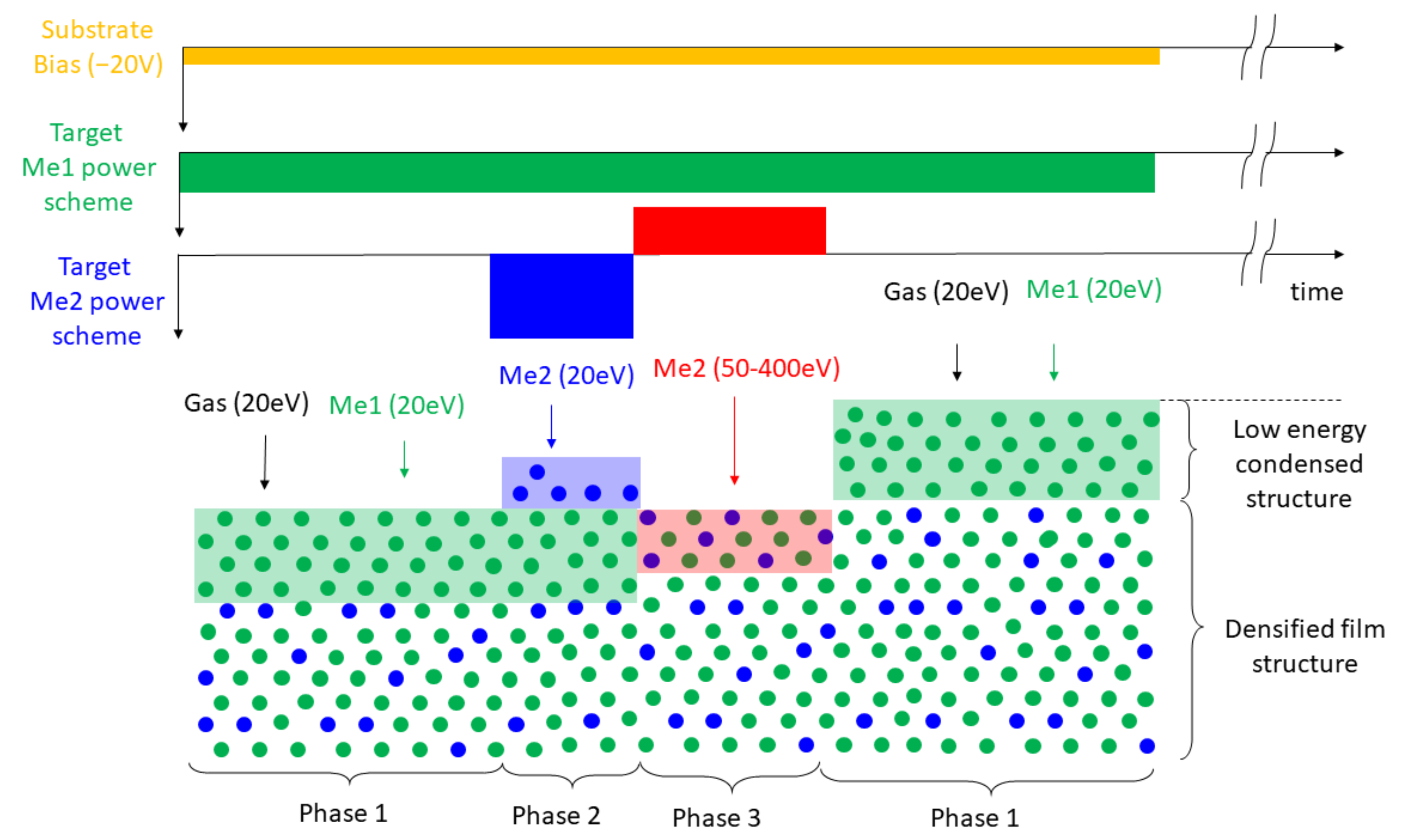
The film growth process consists of three different phases which are intentionally separated in the time domain, as shown in
Figure 1. A simple case with two different metals (Me1, Me2) sputtered in the presence of noble and reactive gases (Argon and Nitrogen) is explained. Me1 means the material of the target operated in DCMS while Me2 means the material of the HIPIMS target. Even though the primarily use of this method would be for TM nitrides such as TiAlN, it can be extended to a wide type of coatings able to be performed by magnetron sputtering such as refractory metals, oxides, carbides, or borides.
- (i)
In Phase 1, a flux of Me1 atoms with low ionization—intrinsic to DCMS discharges—is deposited onto the low voltage biased substrate, typically as low as −20 V which is in the range of the substrate floating potential under a DCMS discharge. This reduced Bias voltage value allows the low energy acceleration of the small fraction of ionized Me1 as well as the noble and reactive gases present in the system. This growing phase gives rise to the deposition of a thermodynamically stable phase with intrinsic poor mechanical properties. But, on the other hand, it minimizes the amount of noble gas—argon in this case- incorporated into the growing film which typically leads to high accumulated stress.
- (ii)
In Phase 2, the HIPIMS magnetron discharge is ignited by applying the negative voltage pulse to the second magnetron, giving rise to the generation of a highly ionized Me2 ion discharge. In static configuration as shown in
Figure 1, Me1 and Me2 irradiation coexist during this short period of time, being in which Me2 also accelerated towards the substrate with an energy proportional to the bias voltage. However, in a dynamic deposition process, Me1 and Me2 are deposited sequentially—magnetrons are placed at different chamber position—and the substrate travels inside the chamber between the different plasma positions.
- (iii)
In Phase 3, a positive pulse is applied to the HIPIMS magnetron. This allows the acceleration of Me2 with high energy towards the growing film, which could lead to the densification of the material deposited between the HIPIMS positive pulses (Me1) or even sub-plantation of Me2 ions into the Me1 matrix for high energy ranges (>100 eV). The Me2 selection might vary from light metal ions such as Al for the sub-plantation of Al+ ions giving rise to metastable cubic TiAlN coatings with high Al content (up to 66%at), to heavy metal ions such as Mo, Nb, or W to promote film densification through effective low energy recoil.
Figure 1.
Schematics of the film growth process consisting in three different phases which are intentionally separated in the time domain.
Figure 1.
Schematics of the film growth process consisting in three different phases which are intentionally separated in the time domain.
This growth model is valid for systems with static or dynamic deposition, such as in the case of a batch coater where the substrate is also exposed sequentially to the different plasmas present in the chamber. The growing film is sequentially exposed to the combination of low ionized and low energetic deposition performed by DCMS and high energetic metal impingement. It is clear to the authors that despite the ion mass, other parameters such as ionization potential, gas rarefaction, reactivity towards nitrogen will affect or the large transit time between the different species are affecting the relative metal/gas ion ratio at the substrate which may in turn affect the changes to crystal structure. This paper will be an initial paper demonstrating the possibilities of this technology which will be followed by a series of work devoted to have a better understanding of the phenomena happening at the substrate position for different metal species.
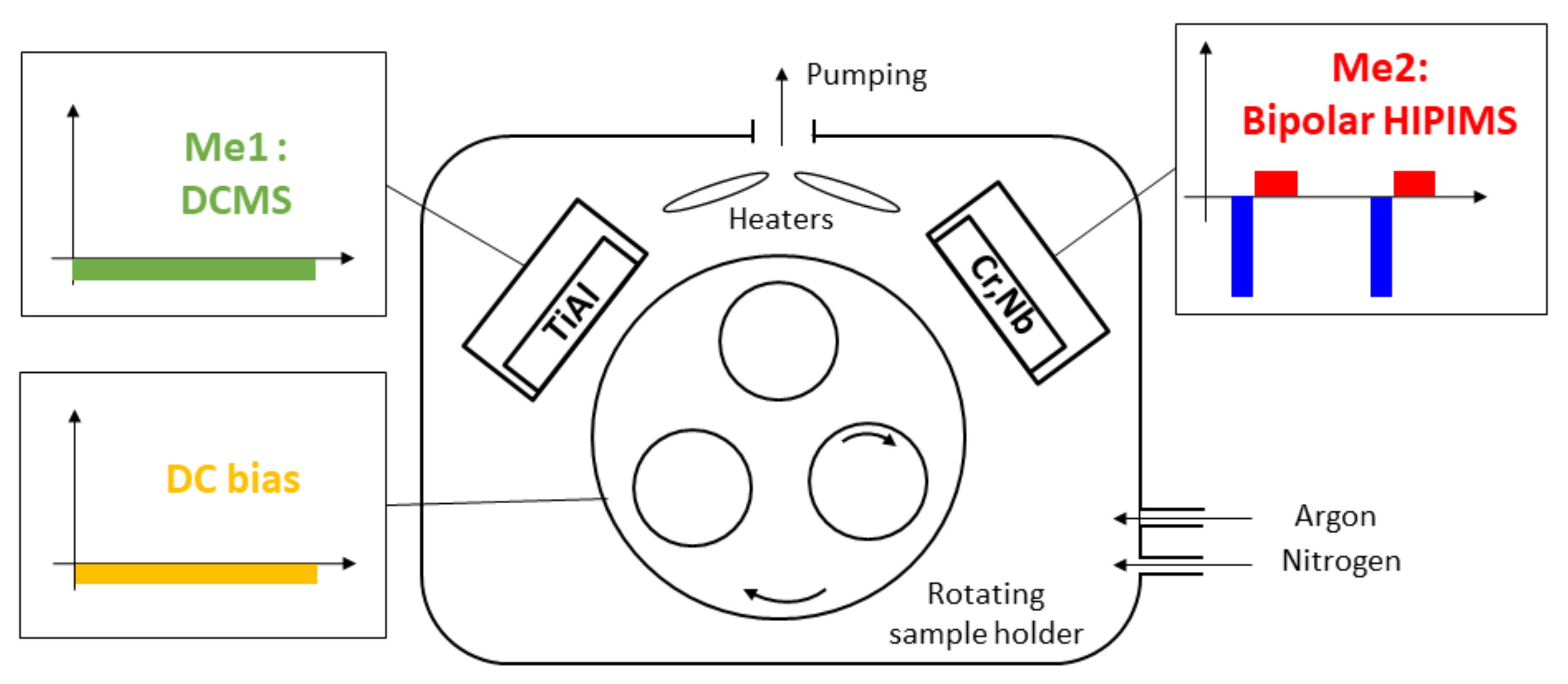
An industrial batch coater with rectangular magnetrons is used for the experiments (
Figure 2). A TiAl target (pressed powder, 50:50 at%) is selected for the deposition of the TiAlN reference film material by DCMS. A Gencoa (Liverpool, UK) rectangular magnetron (400 mm × 100 mm) with a balanced magnetic field configuration which results in a very low bombardment to the depositing film is used for the TiAlN deposition. A second rectangular magnetron (400 mm × 100 mm) with strong unbalanced configuration is employed to generate and accelerate the metal ions (Me2 as described in the above section). Elements with large difference in mass are selected to evaluate the effect of the metal ion impinging on the resulting TiAl(1−x)Me2(x)N film properties: niobium (Nb)—
mNb = 92.9 amu, and chromium (Cr)—
mCr = 52.0 amu. A 10 kW HipV power supply with positive pulse capacity is employed to feed the HIPIMS cathode, while an AE Pinnacle power supply is used for the DCMS. A HipV bias power supply is employed to apply the low voltage straight DC bias (−20 V and −70 V). The substrate table consist of three spindles of 150 mm diameter each connected to a 350 mm rotating table. The substrates are clamped in the different spindles and subject to 2-fold rotation during deposition.
The film characterization was carried out in a set of different substrates: Silicon (001) wafers were used for the thickness, morphology, and composition measurements in SEM-EDX; electropolished 304 L stainless steel (50 × 50 mm2) for the XRD characterization; M2 HSS coupons (10 mm diameter) for the nanoindentation hardness measurement; thin steel strips (0.1 mm thickness, 40 mm length and 5 mm width) for the stress calculation using Stoney’s equation.
Two different series of TiAl(1 − x)Me2(x)N (Me2: Cr, Nb) were deposited to evaluate the effect of mass and energy of the metal ion impinging the TiAlN matrix deposited. A straight DC bias of −70 V was applied during deposition. Also, a third (TiAl)1−xNbxN sample was deposited with a straight Bias as low as −20 V for comparison with the series at −70 V Bias.
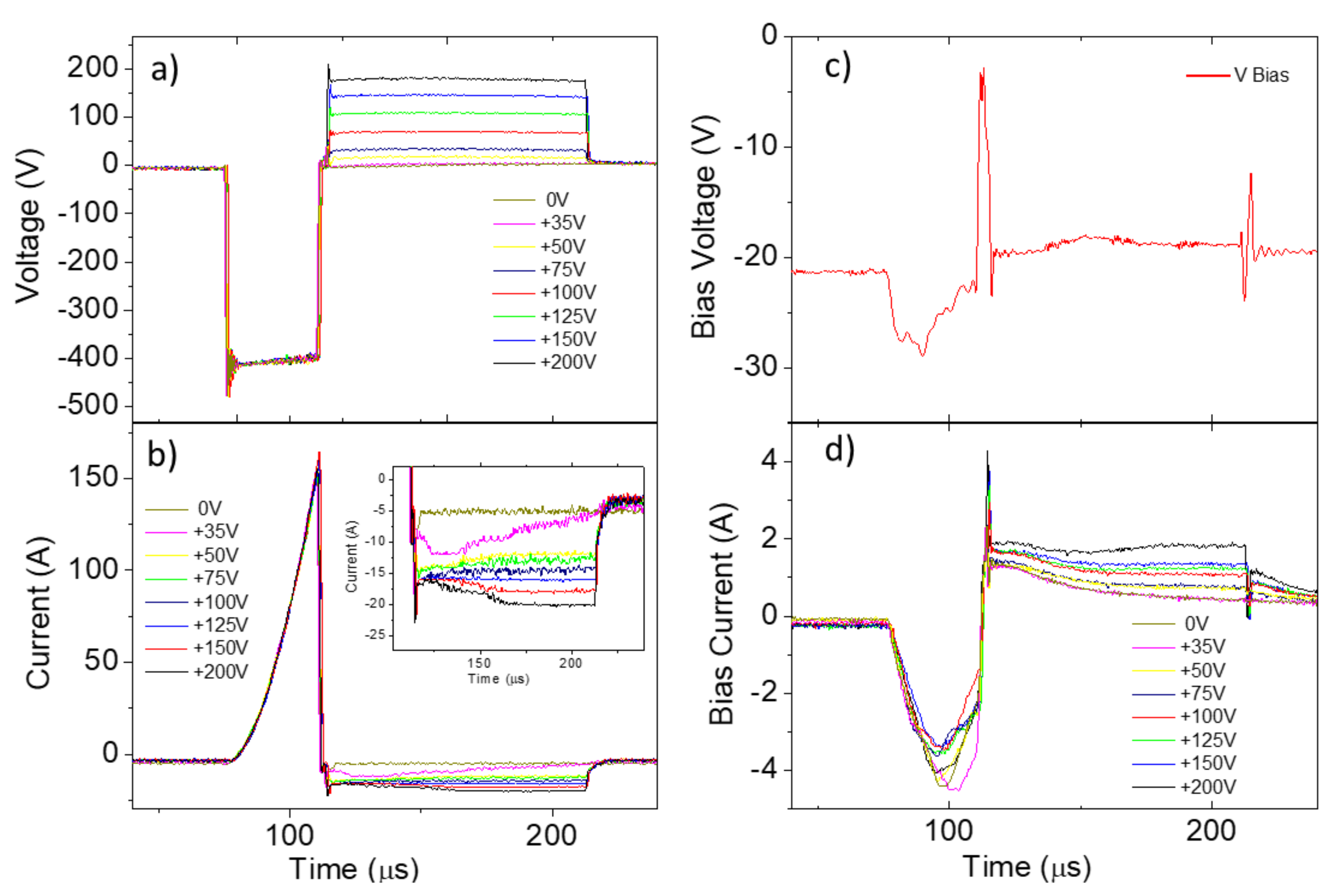
After 1 h heating at 300 °C, a pulsed argon glow discharge (450 V–150 kHz) is applied for 30 min prior to film deposition to remove the substrates contaminants and native oxide, followed by a thin Me2 (Nb or Cr) bonding layer deposited by HiPIMS for 5 min. The same HIPIMS power supply and pulsing parameters are used for both the bonding layer and the subsequent metal nitride irradiation to ensure process stabilization during nitrogen addition, so as the amplitude of the positive pulse is also varied during bonding layer deposition in the series. The Me2 average power was adjusted to have a similar concentration of Me2 in the films x = Me2/(Al + Ti + Me2)—in the range of 0.1—and compare the effect of ion mass in the mechanical properties of the resulting film. This assumption results in an average power of 1.5 kW for Nb, and 1.0 kW in the case of Cr. The pulsing parameters were the same in both cases: negative pulse width: 35 us, positive pulse width: 100µs; repetition frequency: 1 kHz); delay between negative and positive pulse: 3 µs; the amplitude of the positive pulse (Vpos) was varied between 0 V and +200 V; repetition frequency: 1 kHz). The following operating voltage and peak current were obtained during deposition: 540 V–110 A (0.28 A/cm2) for Cr, and 630 V–160 A (0.40 A/cm2) for Nb.
In all cases, the TiAlN matrix was deposited on DCMS with a constant average power of 3 kW (350 V–8.5 A) as well as gas flows (Ar = 56 sccm, N2 = 24 sccm), giving rise to a total pressure of P(Ar + N2) = 7 × 10⁻³ mbar. The rotation speed is maintained at 5 rpm.
The selection of pulsing parameters (in both the positive and negative phases) was based on the experiments published in [
11], where it is demonstrated that the application of a short negative pulse followed by a larger positive pulse maximizes the fraction of positive ions accelerated during the positive phase. As the negative pulse time is longer than the time-of-flight of the metal ions, these ions reach the substrate without being accelerated. Obviously, this parameter selection depends on the target-to-substrate distance, which ranges between 8 to 15 cm in the current system configuration.
The TiAlN deposition rate is calculated to be approximately 2.5 µm/h. Based on the previous results in the same batch coater, it is assumed that most of the film material would be deposited when the substrate faces the operating magnetron (in this case, the TiAl DCMS), thus, a TiAlN nano-layer of a maximum thickness of 3.3 nm would be deposited on each pass (approximately 8 ML) [
12]. Still, it is well known for batch coaters that a certain degree of depositing material reaches the substrate in off-angle positions or at positions very distant from the ignited magnetron, so further investigations to identify the accurate nano-layer thickness should be carried out by, for example, transmission electron microscopy. In the case of the metal ions (Me2), a low thickness <1 monolayer is expected as corroborated from the composition measurements showing an element atomic composition TiAl(1−x)Me2(x)N, x < 10% at%.
Samples are labelled as (Cr,Nb)xVByV in the graphs, being x the positive voltage amplitude (x= 0 V, +50 V, +100 V and +200 V for Nb and x = 0 V, +50 V and +200 V for Cr) and y the bias voltage used for deposition (x = −20 V and −70 V).
3.2. Coating Properties
The atomic composition of the (TiAl)
1−x(Cr,Nb)
xN films deposited onto silicon is shown in
Table 1. The power levels of the DCMS TiAlN magnetron (3 kW) and the bipolar HiPIMS cathodes (1 kW for Cr, 1.5 kW for Cr) was adjusted to obtain a the composition fraction of Cr and Nb into the (TiAl)
1-x(Cr,Nb)
xN film is around 10 at%. The argon to nitrogen ratio was selected to provide a stoichiometric transition metal nitride film (N2/Ar flow ratio of 0.42). On the other hand, there are no changes in deposited film deposition as a function of the positive pulse. This means that the energetic metal ions incorporate into the TiAlN matrix without creating a distortion in the Al to Ti ratio, which remains constant for the different Me2 ion energies. The relatively high oxygen content of the reference TiAlN might be related with the high film porosity of the TiAlN matrix (deposited with low ion bombardment) and the subsequent oxidation after exposure to air. This assumption is corroborated with the columnar structure found with the SEM cross sections as well as the poor mechanical properties measured by nanoindentation (see
Figure 4a and
Figure 5a). The oxygen signal disappears as soon as the energetic Cr o Nb metals are incorporated.
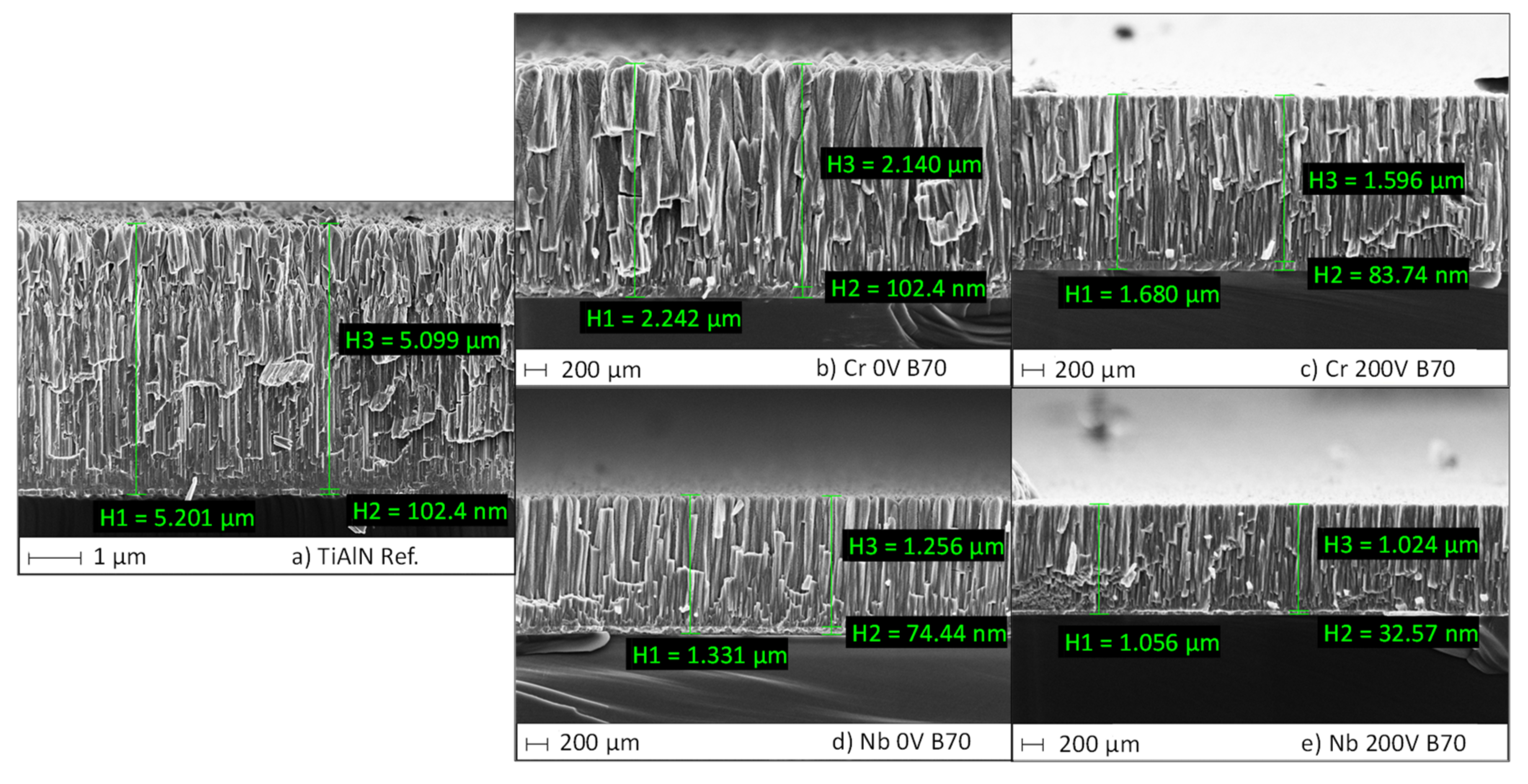
The fracture cross sections SEM images for the reference TiAlN, sample as well as the selected (TiAl)
1−x(Cr,Nb)
xN samples with no positive and
Vpos = +200 V accelerating voltage are shown in
Figure 4. Even though the films remain with a clear columnar morphology for the increasing positive pulse amplitudes, a reduction in the film roughness is observed for the samples exposed to the selective metal ion irradiation. This is also accompanied with a reduction of the deposition rate, as the reference deposition rate for the TiAlN DCMS sample is 2.5 µm/h, dropping to 0.8 µm/h and 0.5 µm/h for both Cr and Nb accelerated with a positive voltage of +200 V. The decrease in deposition rate is attributed to a combination of re-sputtering and densification of the growing film upon metal ion irradiation.
The resulting mechanical properties of the (TiAl)
x(Cr,Nb)
1−xN films are presented in
Figure 4. The nanoindentation hardness as well as the accumulated stress is plotted as a function of the positive accelerating voltage for a sample preparation DC bias voltage of −70 V. Also, a (TiAl)
1−x(Nb)
xN film deposited with a bias voltage of −20 V is included for comparison purposes.
Two different behaviors are observed depending on the ion chosen for irradiating the samples, namely Nb or Cr. In the case of Cr, the hardness increases from 7 GPa to 22 GPa as the positive pulses goes from 0 to +200 V. This trend is expected due to the higher densification (low-energy recoil creation) as the energy of the Cr ions increases. It is also worth mentioning that this film densification is not accompanied by an increase in the film stress (see
Figure 5b), which is a good signature of the metal ion irradiation as compared to the conventional Ar ion assistance on DCMS processes resulting in Ar gas entrapment and high compressive stress.
On the other hand, the Nb irradiated films show an opposite behavior: even though the films present a denser structure as observed on the SEM pictures (see
Figure 3d,e) a linear reduction of hardness accompanied with a linear increase of the film stress is observed. Moreover, the sample deposited with no Nb acceleration voltage already shows a high hardness value of 25 GPa as compared to the same sample deposited with Cr. This would imply that the initial selection of parameters for the heavy mass ion (Nb) were too energetic to maintain the good mechanical properties. Thus, for comparison, a (TiAl)
1-x(Nb)
xN film was deposited with a lower Bias voltage of −20 V and +50 V acceleration voltage. In this case, a higher hardness value of 25 GPa is observed together with a high compressive stress value of −2.5 GPa.
It is well known that Ti50Al50N forms a metastable cubic phase, posing an important challenge regarding phase stability. Under strong ion irradiation conditions, the precipitation of the cubic TiAlN phase into wurtzite AlN phase can be observed, thus hindering the film mechanical properties.
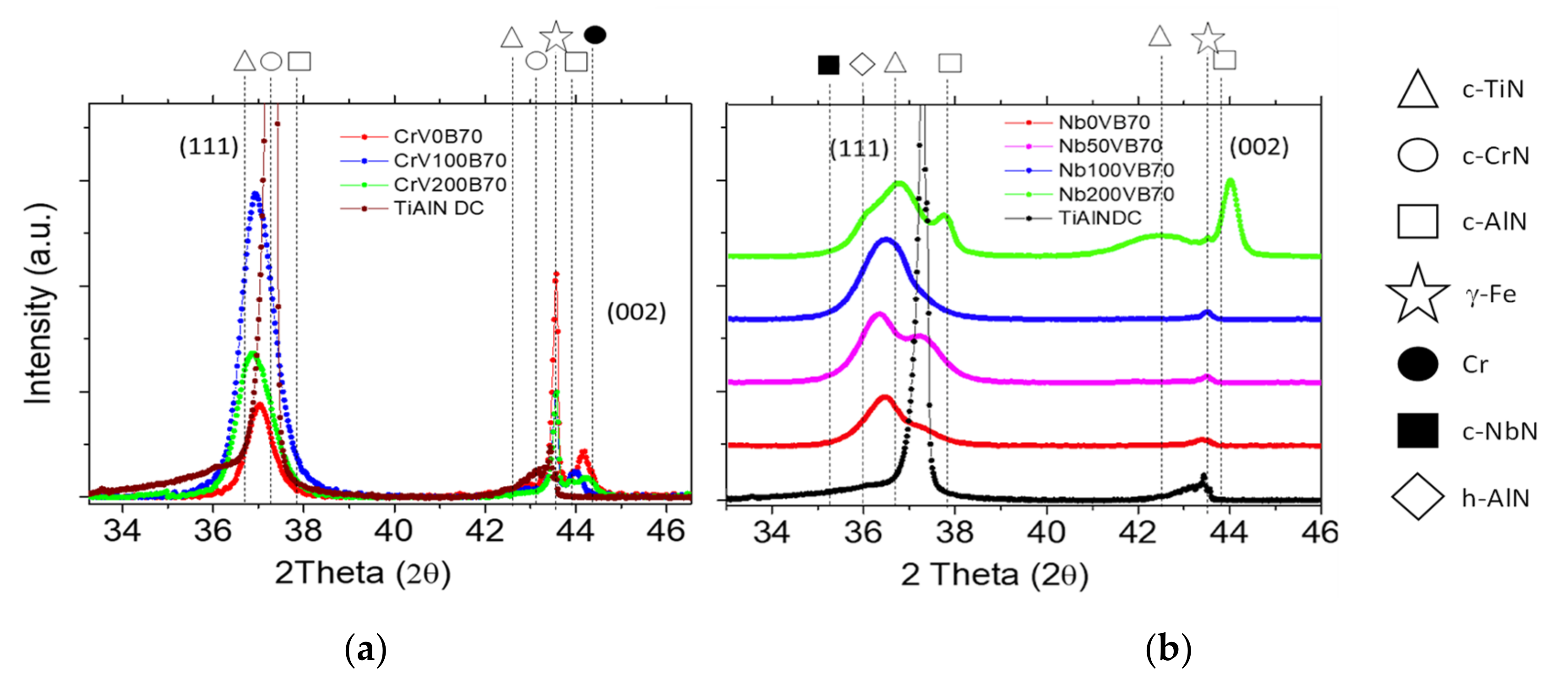
The XRD patterns of the (TiAl)
1−x(Cr)
xN and (TiAl)
1−x(Nb)
xN films as a function of the applied positive pulse are shown in
Figure 6a,b, respectively. The XRD pattern of a TiAlN DCMS film deposited under similar conditions is also shown for reference. The peaks at 2θ ≈ 43.5° corresponds to the γ-Fe lattice coming from the steel substrate in all cases.
TiAlN films are often composed by a single face-centered cubic phase, corresponding to the δ-Ti(Al)N rock-salt B1 crystal structure [
13], as shown in the TiAlN DC pattern by the appearance of the peaks situated at 2θ ≈ 37.3° and 2θ ≈ 43.5°. These peaks correlate to the (111) and (200) found in the face-centered cubic crystalline systems. The intensity of the (111) peak is very high, denoting a predominant (111) growth orientation over the (200), and a high degree of crystallinity with large grains present in the coating with similar composition. The (200) peak, however, is broader and lower in intensity than the (111), which might be the resultant from much lower size crystals showing this orientation.
In the case of the (TiAl)
1−x(Cr)
xN XRD spectra (
Figure 6a), three peaks are shown at 2θ ≈ 37.3°, 2θ ≈ 43° and 2θ ≈ 44°. The peaks appearing at 2θ ≈ 37.3° and 2θ ≈ 43° are correlated with the (111) and (200) diffraction planes from a single-phase face-centered cubic structure. In this phase, the Cr atoms could insert in the TiAlN matrix replacing either the Ti or the Al atoms. The (111) peak, although still being the highest in intensity, is broader and much lower in intensity when compared to the original TiAlN DCMS XRD pattern, pointing out that these coatings are overall less crystalline and are composed of smaller grains with an array of different Ti
xAl
yCr
zN compositions. When comparing the shape of the peaks as a function of the positive pulse voltage, it can be seen that the (111) peak changes in intensity; from the lowest at 0 V; to the highest at 100 V, to then drop down again at 200 V. This phenomenon could indicate that the energy of the incident metallic atoms at 100 V is enough to compress and densify the film via the low-energy recoil, maintaining the cubic (111) orientation with bigger crystal grains. On the other hand, the higher energy of the incident atoms at 200 V is superior and could promote the destruction of the cubic lattice, resulting in smaller crystal grains and the amorphization of the film. It must be noted that the (111) peaks also shift to lower diffraction angles as the voltage of the positive pulses is increased, which could be the result of the higher-energy incident atoms inducing higher compressive stress to the coatings, as can be observed in
Figure 5b. The peak that appears at 2θ ≈ 44° can be correlated with the (200) peak from the pure Cr bonding layer that was deposited to enhance the adhesion in this series. As explained in the experimental section, the positive pulse was also applied during bonding layer deposition to ensure process stabilization during the nitrogen addition, which might explain the shift of the diffraction peak to lower angles as positive pulse increases. It is also worth mentioning the decrease of the Cr bonding diffraction peak intensity with higher positive pulse voltage amplitudes which follows the same trend with the γ-Fe substrate peak at 2θ ≈ 43.5° which might be related with the increase of (TiAl)
1−x(Cr)
xN density.
In the case of the (TiAl)
1−x(Nb)
xN XRD spectra (
Figure 6b), two peaks can be observed at lower positive pulse voltages at 2θ ≈ 36.5° and 2θ ≈ 37.4°. However, at 200 V positive pulse voltage, five peaks appear at 2θ ≈ 36°, 2θ ≈ 36.5°, 2θ ≈ 37.8°, 2θ ≈ 42.5° and 2θ ≈ 44.3°. The peaks showing at 2θ ≈ 36.5° and 2θ ≈ 42.5° are again correlated to the (111) and (200) peaks present in face-centered cubic lattices but are heavily displaced to lower diffraction angles which could be a result of the combined effect from the higher compressive stress developed in the coatings after ion bombardment and Nb being inserted in the TiAlN matrix. The peak that appears at 2θ ≈ 37.4° at lower positive pulse voltages can be assigned to the (110) peak from
c-Nb, present in the Nb bonding layer deposited in this series. At 200 V positive pulse, as the energy from the incident atoms is very high, the metastable cubic lattice suffers a spinodal decomposition resulting in cubic Ti-rich and Al-rich phases, which can be denoted by the peaks appearing at 2θ ≈ 36.5° and 42.5° (cubic Ti-rich phase) and 2θ ≈ 37.8° and 44.3° (cubic Al-rich phase). The decomposition of the metastable cubic lattice implies a drop in mechanical properties and the appearance of a hexagonal wurtzite-type B4 AlN phase at 2θ ≈ 36° [
14] further decreases its performance. Overall, the peaks on the (TiAl)
1−x(Nb)
xN XRD patterns are broad and of low intensity, again showing the low crystallinity and inhomogeneous composition nature of these films.
4. Conclusions
The concept of selective metal ion bombardment using bipolar HIPIMS has been introduced and experimentally demonstrated. The process consists of the combination of conventional DCMS deposition of a transition metal nitride matrix (TiAlN in this particular case) with the subsequent irradiation with metal ions a different kinetic energy. Two distinct metal ions having a large difference in atomic mass were selected: Nb and Cr. The positive acceleration voltage was varied from 0 to +200 V. The resulting film mechanical and microstructural properties were correlated with the plasma parameters, mainly, with the metal ion acceleration voltage.
In all the cases, films showed densification as the acceleration voltage increases while maintaining a low atomic composition content of the irradiating metal in the resulting film (<10 at%). Under these conditions, the results for the light metal ion are more promising. The Cr bombardment allows a hardness improvement from 7 to 22 GPa as well as a reduced film accumulated stress at the highest positive acceleration voltage. From the XRD measurements it is observed that the Cr atoms are inserted into the TiAlN cubic matrix maintaining its crystalline structure. However, the bombardment with the high-mass metal ion (Nb) promotes the deformation of the cubic TiAlN matrix, resulting in a spinodal decomposition and further degradation of the crystalline structure with the appearance of the hexagonal wurtzite-type Al-rich phase. This is also translated to the resulting film mechanical properties, as hardness rapidly decrease from 25 to 10 GPa and stress raises linearly with the positive voltage acceleration. This does not mean that under other deposition conditions the use of heavier metal ions cannot produce transition metal nitride coatings with improved mechanical properties, for example, using much lower metal ion energies or doses.
The paper aims to demonstrate a novel PVD deposition method which is very relevant to the hard coating industrial community. The selective metal ion acceleration method allows the deposition of films with optimum mechanical properties as well as reduced accumulated stress compared to films deposited with gas-ion bombardment typical for direct current magnetron sputtering (DCMS) in a standard industrial batch coater. Applications ranging from low temperature deposition of dense hard coatings (low energy bombardment with heavy metal ions) or low stress- high Al content (Ti,Cr)AlN metastable cubic phases (high energy bombardment and implantation with Al light metal ions) are envisaged for this method.


 ,
, 

