
Magnetron Sputter-Deposited β-Ga2O3 Films on c-Sapphire Substrate: Effect of Rapid Thermal Annealing Temperature on Crystalline Quality


Abstract
:1. Introduction
2. Experimental Details
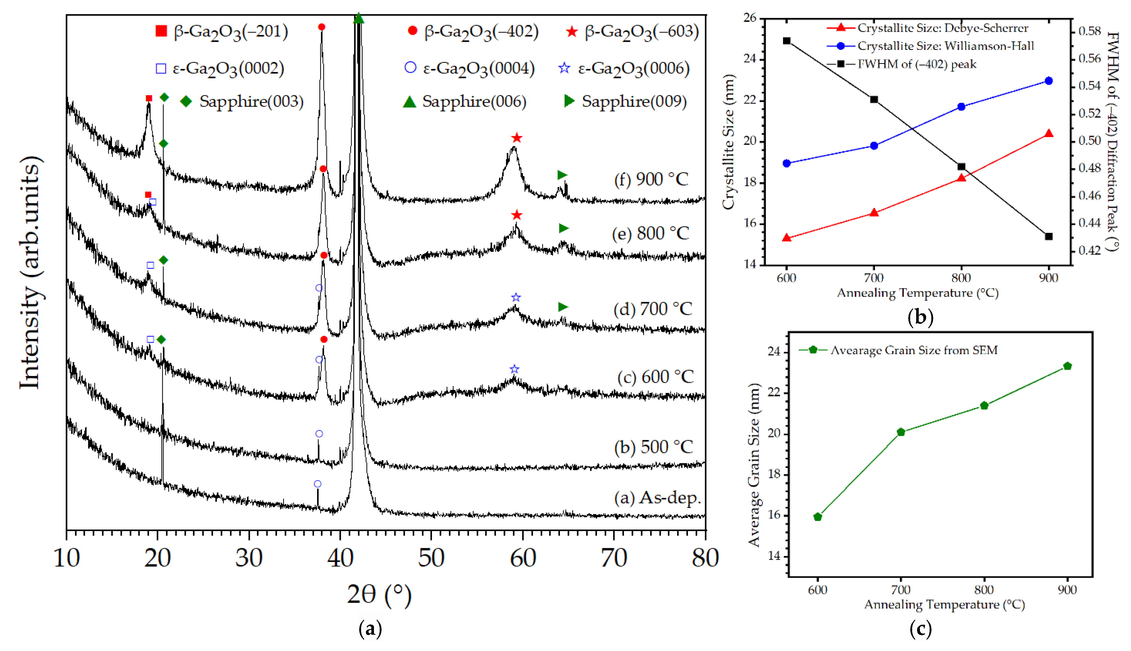
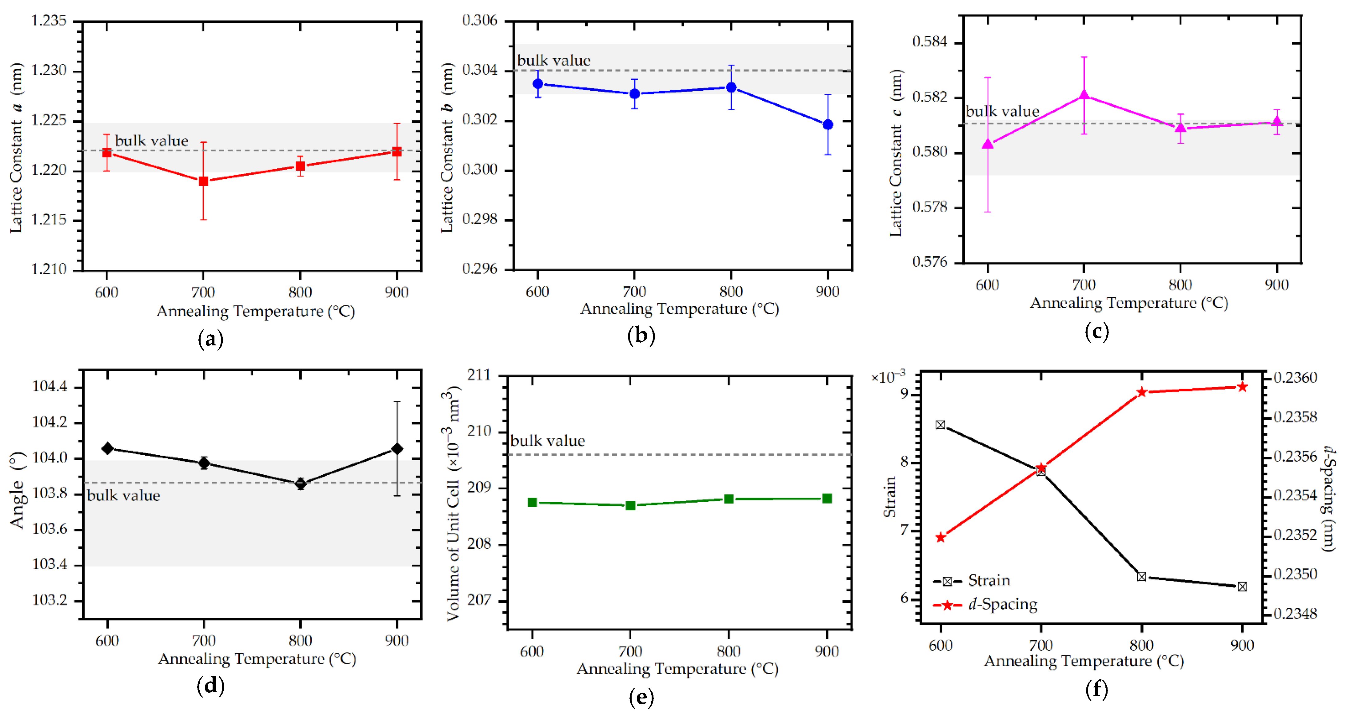
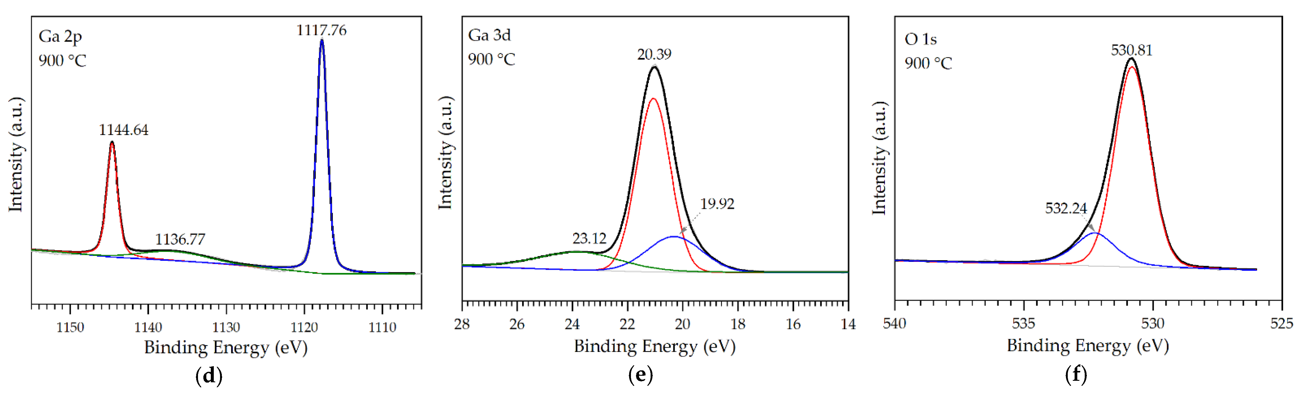
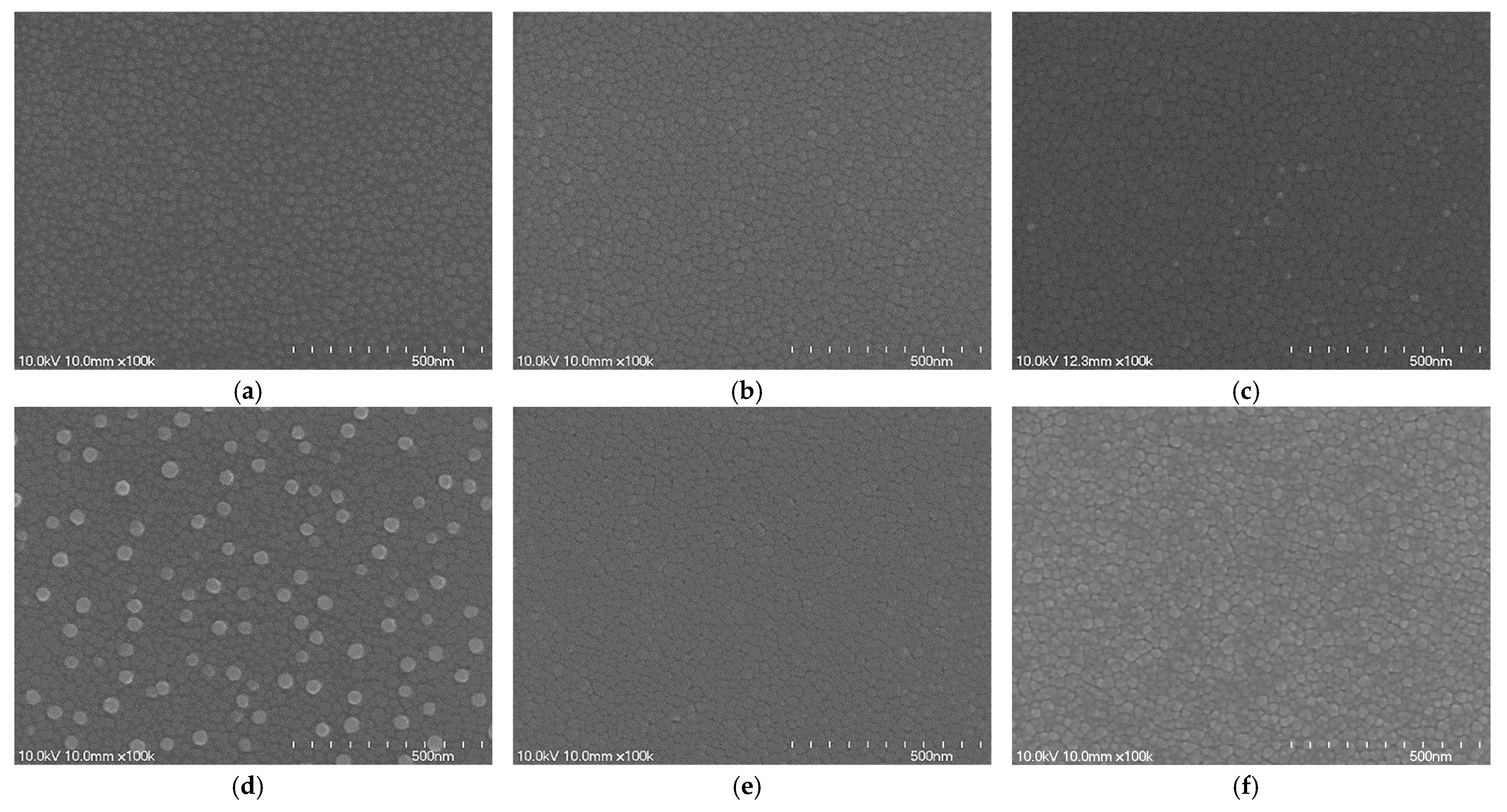
3. Results and Discussion
4. Conclusions
Supplementary Materials
Author Contributions
Funding
Institutional Review Board Statement
Informed Consent Statement
Data Availability Statement
Conflicts of Interest
References
- Saikumar, A.K.; Nehate, S.D.; Sundaram, K.B. Review—RF Sputtered Films of Ga2O3. ECS J. Solid State Sci. Technol. 2019, 8, Q3064–Q3078. [Google Scholar] [CrossRef]
- Wu, J.; Mi, W.; Yang, Z.; Chen, Y.; Li, C.; Zhao, J.; Zhang, K.; Zhang, X.; Luan, C. Influence of annealing on the structural and optical properties of gallium oxide films deposited on c-sapphire substrate. Vacuum 2019, 167, 6–9. [Google Scholar] [CrossRef]
- Bosi, M.; Mazzolini, P.; Seravalli, L.; Fornari, R. Ga2O3 polymorphs: Tailoring the epitaxial growth conditions. J. Mater. Chem. C 2020, 8, 10975–10992. [Google Scholar] [CrossRef]
- Xue, H.; He, Q.; Jian, G.; Long, S.; Pang, T.; Liu, M. An Overview of the Ultrawide Bandgap Ga2O3 Semiconductor-Based Schottky Barrier Diode for Power Electronics Application. Nanoscale Res. Lett. 2018, 13, 290. [Google Scholar] [CrossRef] [PubMed] [Green Version]
- Li, M.Q.; Yang, N.; Wang, G.G.; Zhang, H.Y.; Han, J.C. Highly preferred orientation of Ga2O3 films sputtered on SiC substrates for deep UV photodetector application. Appl. Surf. Sci. 2019, 471, 694–702. [Google Scholar] [CrossRef]
- Liu, X.; Liu, Q.; Zhao, B.; Ren, Y.; Tao, B.W.; Zhang, W.L. Comparison of β-Ga2O3 thin films grown on r-plane and c-plane sapphire substrates. Vacuum 2020, 178, 109435. [Google Scholar] [CrossRef]
- Nakagomi, S.; Kokubun, Y. Crystal orientation of β-Ga2O3 thin films formed on c-plane and a-plane sapphire substrate. J. Cryst. Growth 2012, 349, 12–18. [Google Scholar] [CrossRef]
- Ghosh, S.; Srivastava, H.; Rao, P.N.; Nand, M.; Tiwari, P.; Srivastava, A.K.; Jha, S.N.; Rai, S.K.; Singh, S.D.; Ganguli, T. Investigations on epitaxy and lattice distortion of sputter deposited β-Ga2O3 layers on GaN templates. Semicond. Sci. Technol. 2020, 35, 085024. [Google Scholar] [CrossRef]
- Li, W.; Zhang, X.; Meng, R.; Yan, J.; Wang, J.; Li, J.; Wei, T. Epitaxy of III-Nitrides on β-Ga2O3 and Its Vertical Structure LEDs. Micromachines 2019, 10, 322. [Google Scholar] [CrossRef] [Green Version]
- An, Y.; Daiz, L.; Wuy, Y.; Wuy, B.; Zhaoy, Y.; Liuy, T.; Haoy, H.; Liy, Z.; Niuz, G.; Zhangy, J.; et al. Epitaxial growth of β-Ga2O3 thin films on Ga2O3 and Al2O3 substrates by using pulsed laser deposition. J. Adv. Dielectr. 2019, 9, 1950032. [Google Scholar] [CrossRef] [Green Version]
- Son, H.; Choi, Y.; Hong, S.-K.; Park, J.-H.; Jeon, D.-W. Reduction of dislocations in α-Ga2O3 epilayers grown by halide vapor-phase epitaxy on a conical frustum-patterned sapphire substrate. IUCrJ 2021, 8, 462–467. [Google Scholar] [CrossRef] [PubMed]
- Arata, Y.; Nishinaka, H.; Tahara, D.; Yoshimoto, M. Heteroepitaxial growth of single-phase ε-Ga2O3 thin films on c-plane sapphire by mist chemical vapor deposition using a NiO buffer layer. CrystEngComm 2018, 20, 6236–6242. [Google Scholar] [CrossRef]
- Kukushkin, S.A.; Osipov, A.V.; Bessolov, V.N.; Medvedev, B.K.; Nevolin, V.K.; Tcarik, K.A. Substrates for epitaxy of gallium nitride: New materials and techniques. Rev. Adv. Mater. Sci. 2008, 17, 1–32. [Google Scholar]
- Nishinaka, H.; Tahara, D.; Morimoto, S.; Yoshimoto, M. Epitaxial growth of α-Ga2O3 thin films on a-, m-, and r-plane sapphire substrates by mist chemical vapor deposition using α-Fe2O3 buffer layers. Mater. Lett. 2017, 205, 28–31. [Google Scholar] [CrossRef]
- Jinno, R.; Uchida, T.; Kaneko, K.; Fujita, S. Reduction in edge dislocation density in corundum-structured α-Ga2O3 layers on sapphire substrates with quasi-graded α-(Al,Ga)2O3 buffer layers. Appl. Phys. Express 2016, 9, 071101. [Google Scholar] [CrossRef]
- Oda, M.; Kaneko, K.; Fujita, S.; Hitora, T. Crack-free thick (>5 μm) α-Ga2O3 films on sapphire substrates with α-(Al,Ga)2O3 buffer layers. Jpn. J. Appl. Phys. 2016, 55, 1202B4. [Google Scholar] [CrossRef] [Green Version]
- Ngo, T.S.; Le, D.D.; Lee, J.; Hong, S.-K.; Ha, J.-S.; Lee, W.-S.; Moon, Y.-B. Investigation of defect structure in homoepitaxial (-201) β-Ga2O3 layers prepared by plasma-assisted molecular beam epitaxy. J. Alloys Compd. 2020, 834, 155027. [Google Scholar] [CrossRef]
- Liao, Y.; Jiao, S.; Li, S.; Wang, J.; Wang, D.; Gao, S.; Yu, Q.; Li, H. Effect of deposition pressure on the structural and optical properties of Ga2O3 films obtained by thermal post-crystallization. CrystEngComm 2018, 20, 133–139. [Google Scholar] [CrossRef]
- Dong, L.; Jia, R.; Xin, B.; Zhang, Y. Effects of post-annealing temperature and oxygen concentration during sputtering on the structural and optical properties of β-Ga2O3 films. J. Vac. Sci. Technol. A-Vac. Surf. Films 2016, 34, 060602. [Google Scholar] [CrossRef]
- Meng, Y.; Gao, Y.; Chen, K.; Lu, J.; Xian, F.; Xu, L.; Zheng, G.; Kuang, W.; Cao, Z. Annealing induced phase transition and optical properties of Ga2O3 thin films synthesized by sputtering technique. Optik 2021, 244, 167515. [Google Scholar] [CrossRef]
- Kim, S.; Kim, N.-H. Impurity Phases and Optoelectronic Properties of CuSbSe2 Thin Films Prepared by Cosputtering Process for Absorber Layer in Solar Cells. Coatings 2020, 10, 1209. [Google Scholar] [CrossRef]
- Wang, R.X.; Beling, C.D.; Fung, S.; Djurišić, A.B.; Ling, C.C.; Kwong, C.; Li, S. Influence of annealing temperature and environment on the properties of indium tin oxide thin films. J. Phys. D-Appl. Phys. 2005, 38, 2000–2005. [Google Scholar] [CrossRef]
- Lee, J.; Kim, H.; Gautam, L.; He, K.; Hu, X.; Dravid, V.P.; Razeghi, M. Study of phase transition in MOCVD grown Ga2O3 from κ to β phase by ex situ and in situ annealing. Photonics 2021, 8, 17. [Google Scholar] [CrossRef]
- Yao, Y.; Okur, S.; Lyle, L.A.M.; Tompa, G.S.; Salagaj, T.; Sbrockey, N.; Davis, R.F.; Porter, L.M. Growth and characterization of α-, β-, and ε-phases of Ga2O3 using MOCVD and HVPE techniques. Mater. Res. Lett. 2018, 6, 268–275. [Google Scholar] [CrossRef] [Green Version]
- Boschi, F.; Bosi, M.; Berzina, T.; Buffagni, E.; Ferrari, C.; Fornari, R. Hetero-epitaxy of ε-Ga2O3 layers by MOCVD and ALD. J. Cryst. Growth 2016, 443, 25–30. [Google Scholar] [CrossRef]
- Hsu, C.-H.; Geng, X.-P.; Wu, W.-Y.; Zhao, M.-J.; Zhang, X.-Y.; Huang, P.-H.; Lien, S.-Y. Air Annealing Effect on Oxygen Vacancy Defects in Al-doped ZnO Films Grown by High-Speed Atmospheric Atomic Layer Deposition. Molecules 2020, 25, 5043. [Google Scholar] [CrossRef]
- Li, S.; Jiao, S.; Wang, D.; Gao, S.; Wang, J. The influence of sputtering power on the structural, morphological and optical properties of β-Ga2O3 thin films. J. Alloys Compd. 2018, 753, 186–191. [Google Scholar] [CrossRef]
- Oshima, T.; Okuno, T.; Fujita, S. Ga2O3 Thin Film Growth on c-Plane Sapphire Substrates by Molecular Beam Epitaxy for Deep-Ultraviolet Photodetectors. Jpn. J. Appl. Phys. 2007, 46, 7217–7220. [Google Scholar] [CrossRef]
- Xu, Y.; Park, J.-H.; Yao, Z.; Wolverton, C.; Razeghi, M.; Wu, J.; Dravid, V.P. Strain-Induced Metastable Phase Stabilization in Ga2O3 Thin Films. ACS Appl. Mater. Interfaces 2019, 11, 5536–5543. [Google Scholar] [CrossRef]
- Tak, B.R.; Kumar, S.; Kapoor, A.K.; Wang, D.; Li, X.; Sun, H.; Singh, R. Recent advances in the growth of gallium oxide thin films employing various growth techniques-A review. J. Phys. D Appl. Phys. 2021, 54, 453002. [Google Scholar] [CrossRef]
- Ghose, S.; Rahman, S.; Hong, L.; Rojas-Ramirez, J.S.; Jin, H.; Park, K.; Klie, R.; Droopad, R. Growth and characterization of β-Ga2O3 thin films by molecular beam epitaxy for deep-UV photodetectors. J. Appl. Phys. 2017, 122, 095302. [Google Scholar] [CrossRef]
- Jiao, S.; Lu, H.; Wang, X.; Nie, Y.; Wang, D.; Gao, S.; Wang, J. The Structural and Photoelectrical Properties of Gallium Oxide Thin Film Grown by Radio Frequency Magnetron Sputtering. ECS J. Solid State Sci. Technol. 2019, 8, Q3086–Q3090. [Google Scholar] [CrossRef]
- Lv, Y.; Ma, J.; Mi, W.; Luan, C.; Zhu, Z.; Xiao, H. Characterization of β-Ga2O3 thin films on sapphire (0001) using metal-organic chemical vapor deposition technique. Vacuum 2012, 86, 1850–1854. [Google Scholar] [CrossRef]
- Feng, Z.; Huang, L.; Feng, Q.; Li, X.; Zhang, H.; Tang, W.; Zhang, J.; Hao, Y. Influence of annealing atmosphere on the performance of a β-Ga2O3 thin film and photodetector. Opt. Mater. Express 2018, 8, 2229–2237. [Google Scholar] [CrossRef]
- Patterson, A.L. The Scherrer formula for X-ray particle size determination. Phys. Rev. 1939, 56, 978–982. [Google Scholar] [CrossRef]
- Williamson, G.K.; Hall, W.H. X-ray line broadening from filed aluminium and wolfram. Acta Metall. Mater. 1953, 1, 22–31. [Google Scholar] [CrossRef]
- Joshi, G.; Chauhan, Y.S.; Verma, A. Temperature Dependence of β-Ga2O3 Heteroepitaxy on c-plane Sapphire using Low Pressure Chemical Vapor Deposition. J. Alloys Compd. 2021, 883, 160799. [Google Scholar] [CrossRef]
- Mote, V.D.; Purushotham, Y.; Dole, B.N. Williamson-Hall analysis in estimation of lattice strain in nanometer-sized ZnO particles. J. Theor. Appl. Phys. 2012, 6, 6. [Google Scholar] [CrossRef] [Green Version]
- Kumar, S.; Asokan, K.; Singh, R.K.; Chatterjee, S.; Kanjilal, D.; Ghosh, A.K. Investigations on structural and optical properties of ZnO and ZnO: Co nanoparticles under dense electronic excitations. RSC Adv. 2014, 4, 62123–62131. [Google Scholar] [CrossRef]
- Boonlakhorn, J.; Prachamon, J.; Manyam, J.; Krongsuk, S.; Thongbai, P.; Srepusharawoot, P. Colossal dielectric permittivity, reduced loss tangent and the microstructure of Ca1−xCdxCu3Ti4O12−2yF2y ceramics. RSC Adv. 2021, 11, 16396–16403. [Google Scholar] [CrossRef]
- Negi, J.; Panwar, N.S. Structural and electrical properties of lead-free Na0.685K0.315Nb1–yTayO3 (0 ≤ y ≤ 0.05) ceramics. J. Phys. Chem. Solids 2021, 151, 109853. [Google Scholar] [CrossRef]
- Bel, A.M.T.; Clegg, F.; Henderson, C.M.B. Monoclinic–orthorhombic first-order phase transition in K2ZnSi5O12 leucite analogue; transition mechanism and spontaneous strain analysis. Mineral. Mag. 2021, 85, 1–20. [Google Scholar] [CrossRef]
- Geller, S. Crystal Structure of β-Ga2O3. J. Chem. Phys. 1960, 33, 676. [Google Scholar] [CrossRef]
- McCluskey, M.S. Point defects in Ga2O3. J. Appl. Phys. 2020, 127, 101101. [Google Scholar] [CrossRef] [Green Version]
- Marai, A.B.; Belgacem, J.B.; Ayadi, J.B.; Djessas, K.; Alaya, S. Structural and optical properties of CuIn1-xGaxSe2 nanoparticles synthesized by solvothermal route. J. Alloys Compd. 2016, 658, 961–966. [Google Scholar] [CrossRef]
- Goh, K.H.; Haseeb, A.S.M.A.; Wong, Y.H. Physical and electrical properties of thermal oxidized Sm2O3 gate oxide thin film on Si substrate: Influence of oxidation durations. Thin Solid Films 2016, 606, 80–86. [Google Scholar] [CrossRef]
- Rabiei, M.; Palevicius, A.; Monshi, A.; Nasiri, S.; Vilkauskas, A.; Janusas, G. Comparing Methods for Calculating Nano Crystal Size of Natural Hydroxyapatite Using X-ray Diffraction. Nanomaterials 2020, 10, 1627. [Google Scholar] [CrossRef] [PubMed]
- Cora, I.; Mezzadri, F.; Boschi, F.; Bosi, M.; Čaplovičová, M.; Calestani, G.; Dódony, I.; Pécz, B.; Fornari, R. The real structure of ε-Ga2O3 and its relation to κ-phase. CrystEngComm 2017, 19, 1509–1516. [Google Scholar] [CrossRef] [Green Version]
- Shokeen, P.; Jain, A.; Kapoor, A.; Gupta, V. Thickness and Annealing Effects on the Particle Size of PLD Grown Ag Nanofilms. Plasmonics 2016, 11, 669–675. [Google Scholar] [CrossRef]
- Chen, Z.; Wang, X.; Noda, S.; Saito, K.; Tanaka, T.; Nishio, M.; Arita, M.; Guo, Q. Effects of dopant contents on structural, morphological and optical properties of Er doped Ga2O3 films. Superlattices Microstruct. 2016, 90, 207–214. [Google Scholar] [CrossRef]
- Cammarata, R.C. Stresses in thin films. In Surface Modification and Mechanisms: Friction, Stress, and Reaction Engineering, 1st ed.; Totten, G.E., Liang, H., Eds.; Marcel Dekker Inc.: New York, NY, USA, 2005; pp. 20–35. [Google Scholar]
- Zhao, M.-J.; Sun, Z.-T.; Zhang, Z.-X.; Geng, X.-P.; Wu, W.-Y.; Lien, S.-Y.; Zhu, W.-Z. Suppression of Oxygen Vacancy Defects in sALD-ZnO Films Annealed in Different Conditions. Materials 2020, 13, 3910. [Google Scholar] [CrossRef] [PubMed]
- Chikoidze, E.; Rogers, D.J.; Teherani, F.H.; Rubio, C.; Sauthier, G.; Von Bardeleben, H.J.; Tchelidze, T.; Ton-That, C.; Fellous, A.; Bove, P.; et al. Puzzling robust 2D metallic conductivity in undoped β-Ga2O3 thin films. Mater. Today Phys. 2019, 8, 10–17. [Google Scholar] [CrossRef] [Green Version]
- Chen, J.X.; Li, X.X.; Ma, H.P.; Huang, W.; Ji, Z.G.; Xia, C.; Lu, H.L.; Zhang, D.W. Investigation of the Mechanism for Ohmic Contact Formation in Ti/Al/Ni/Au Contacts to β-Ga2O3 Nanobelt Field-Effect Transistors. ACS Appl. Mater. Interfaces 2019, 11, 32127–32134. [Google Scholar] [CrossRef] [PubMed]
- Rafique, S.; Han, L.; Zhao, H. Thermal annealing effect on β-Ga2O3 thin film solar blind photodetector heteroepitaxially grown on sapphire substrate. Phys. Status Solidi A-Appl. Mater. 2017, 214, 1700063. [Google Scholar] [CrossRef]
- Rajamani, S.; Arora, K.; Belov, A.; Korolev, D.; Nikolskaya, A.; Usov, Y.; Pavlov, D.; Mikhaylov, A.; Tetelbaum, D.; Kumar, M.; et al. Enhanced Solar-Blind Photodetection Performance of Encapsulated Ga2O3 Nanocrystals in Al2O3 Matrix. IEEE Sens. J. 2018, 18, 4046–4052. [Google Scholar] [CrossRef]
- Zhuo, Y.; Chen, Z.; Tu, W.; Ma, X.; Pei, Y.; Wang, G. β-Ga2O3 versus ε-Ga2O3: Control of the crystal phase composition of gallium oxide thin film prepared by metal-organic chemical vapor deposition. Appl. Surf. Sci. 2017, 420, 802–807. [Google Scholar] [CrossRef]
- Schewski, R.; Wagner, G.; Baldini, M.; Gogova, D.; Galazka, Z.; Schulz, T.; Remmele, T.; Markurt, T.; Von Wenckstern, H.; Grundmann, M.; et al. Epitaxial stabilization of pseudomorphic α-Ga2O3 on sapphire (0001). Appl. Phys. Express 2014, 8, 011101. [Google Scholar] [CrossRef]
- Prokes, S.M.; Katz, M.B.; Twigg, M.E. Growth of crystalline Al2O3 via thermal atomic layer deposition: Nanomaterial phase stabilization. APL Mater. 2014, 2, 032105. [Google Scholar] [CrossRef]
- Rentenberger, C.; Waitz, T.; Karnthaler, H.P. HRTEM analysis of nanostructured alloys processed by severe plastic deformation. Scr. Mater. 2004, 51, 789–794. [Google Scholar] [CrossRef]
- Zhang, Z.; Ódor, É.; Farkas, D.; Jóni, B.; Ribárik, G.; Tichy, G.; Nandam, S.H.; Ivanisenko, J.; Preuss, M.; Ungár, T. Dislocations in grain boundary regions: The origin of heterogeneous microstrains in nanocrystalline materials. Metall. Mater. Trans. A-Phys. Metall. Mater. Sci. 2020, 51, 513–530. [Google Scholar] [CrossRef] [Green Version]


Publisher’s Note: MDPI stays neutral with regard to jurisdictional claims in published maps and institutional affiliations. |
© 2022 by the authors. Licensee MDPI, Basel, Switzerland. This article is an open access article distributed under the terms and conditions of the Creative Commons Attribution (CC BY) license (https://creativecommons.org/licenses/by/4.0/).
Share and Cite
Pech, S.; Kim, S.; Kim, N.-H. Magnetron Sputter-Deposited β-Ga2O3 Films on c-Sapphire Substrate: Effect of Rapid Thermal Annealing Temperature on Crystalline Quality. Coatings 2022, 12, 140. https://doi.org/10.3390/coatings12020140
Pech S, Kim S, Kim N-H. Magnetron Sputter-Deposited β-Ga2O3 Films on c-Sapphire Substrate: Effect of Rapid Thermal Annealing Temperature on Crystalline Quality. Coatings. 2022; 12(2):140. https://doi.org/10.3390/coatings12020140
Chicago/Turabian StylePech, Sakal, Sara Kim, and Nam-Hoon Kim. 2022. "Magnetron Sputter-Deposited β-Ga2O3 Films on c-Sapphire Substrate: Effect of Rapid Thermal Annealing Temperature on Crystalline Quality" Coatings 12, no. 2: 140. https://doi.org/10.3390/coatings12020140
APA StylePech, S., Kim, S., & Kim, N.-H. (2022). Magnetron Sputter-Deposited β-Ga2O3 Films on c-Sapphire Substrate: Effect of Rapid Thermal Annealing Temperature on Crystalline Quality. Coatings, 12(2), 140. https://doi.org/10.3390/coatings12020140