Article

Comparative Study of High-Temperature Annealed and RTA Process β-Ga2O3 Thin Film by Sol–Gel Process

1
Department of Intelligent Energy and Industry, Chung-Ang University, Seoul 06974, Korea
2
School of Electrical and Electronics Engineering, Chung-Ang University, Seoul 06974, Korea
*
Author to whom correspondence should be addressed.
Coatings 2021, 11(10), 1220; https://doi.org/10.3390/coatings11101220
Submission received: 7 September 2021 / Revised: 30 September 2021 / Accepted: 2 October 2021 / Published: 5 October 2021
(This article belongs to the Special Issue Semiconductor Thin Films)

Abstract

:
As a wide energy band gap semiconductor, a Ga2O3 thin film was prepared by the sol–gel process with different annealing processes. Since Ga2O3 is a type of metal oxide structure, an oxygen annealing process can be considered to remove oxygen defects. An effective oxygen annealing process can help form a β-Ga2O3 structure with reduced defects. In this study, different types of annealing effects for β-Ga2O3 were investigated and compared. An electric furnace process using thermal effect characteristics of and an Rapid Thermal Annealing (RTA) process applied with an infrared radiation light source were compared. Two and 4 h thermal annealing processes were conducted at 900 °C in the furnace. Meanwhile, to study the optical annealing effects, 2 h furnace at 900 °C + 15 min in rapid thermal annealing and only 15 min in rapid thermal annealing effects were compared, respectively. Through increasing the thermal annealing temperature and time, β-Ga2O3 can be formed even though a sol–gel process was employed in this experiment. An annealing temperature of at least 900 °C was required to form β-Ga2O3 thin film. Moreover, by introducing an RTA process just after the spinning process of thin film, a β-Ga2O3 thin film was formed on the sapphire substrates. Compared with the electric furnace process applied for 2 h, the RTA process performed in 15 min has a relatively short process time and results in similar structural and optical characteristics of a thin film. From the X-ray diffraction patterns and UV spectrometer analysis, optically annealed β-Ga2O3 thin films on the sapphire substrate showed a highly crystalized structure with a wide energy band gap of 4.8 eV.

Graphical Abstract

1. Introduction

Currently, the energy industry is changing to renewable energy and focusing on carbon-free and power saving. For future industries on which internet of things (IoT) and artificial intelligence (A.I.) technologies are based, there will be increased interest in the effective control of high power and saving. In order to meet these demands, the importance of power devices is growing. Power device are emerging that use a reduced amount of electricity and use energy efficiently [1]. Next-generation power semiconductor materials have superior power efficiency and durability compared to silicon. As the demand for electronic devices and power consumption increase, the power semiconductor industry has high potential for future growth. GaAs (1.43 eV) and GaN (3.4 eV) have been investigated for wide band gap materials, [2,3], but they are suitable as LED elements and power switching. Another possible material, SiC (3.26 eV), has been employed as an emerging material [4] for power devices such as power diodes and transistors. However, in future industries, ultra-wide bandgap materials are preferred to control high-power systems [5] such as industrial assembly robots, electric vehicles and energy storage systems. These materials contain diamond, boron nitride, Al-AlGaN, and β-Ga2O3. Of these ultra-wide band-gap materials [6], monoclinic structured β-Ga2O3 is drawing attention as a next-generation power device material due to its various properties and feasibility. In general, Ga2O3 has been studied for different forms of crystal structures known as identification polymorphs and consists of α, β, γ, δ, and ε crystal structures and the β phase is recognized as the most stable award in the five phases. Above 600 °C, all Ga2O3 phases converge in beta. Therefore, β is the most thermally and chemically stable phase [7,8,9]. Moreover, there has been a growing body of investigations that obtain β-Ga2O3 thin film by various methods, including chemical vapor deposition (CVD), plasma-enhanced atomic layer deposition (PEALD), radio frequency sputtering (RF sputtering), molecular beam epitaxy (MBE), hydride vapor phase epitaxy, and pulsed laser deposition (PLD) [10,11,12,13,14]. However, these processes are not suitable for large-area production, because they are vacuum-based complex methods. Compared to other thin film processes, the sol–gel method requires low cost to obtain large-scale application. Moreover, this process can be applied to most types of materials. β-Ga2O3 is an ultra-wide band-gap material of 4.8 eV that has semiconductor properties [15]. In order to obtain the β phase, a high-temperature oxygen annealing process should be applied. Under high-temperature processing conditions, the β-Ga2O3 material has unique semiconductor property [16]. Annealing is the one of the most important processes of semiconductor manufacturing, because semiconductors can have improved electrical and structural properties by heating and cooling the material to remove defects in the materials [17,18]. During the thin film annealing process, it requires a lot of energy when the process is performed in a furnace. Especially, high temperature with a long processing time can induce structural deformation. In general, compared to the existing experiment, it has various advantages such as economic aspects in the case of a low-temperature process or a fast process. If an annealing process can be carried out through RTA (Rapid Thermal Annealing), the processing time and energy can be decreased drastically. In this experiment, RTA was performed to replace the furnace in the annealing process to crystallize β-Ga2O3. Many papers reported that β-Ga2O3 thin films can be obtained by employing the post-annealing process [19,20]. To obtain β-Ga2O3 thin film through the post-annealing process, more than 700 °C of annealing temperature was required. However, this high-temperature annealing process with a long time can degenerate the crystalline properties of Ga2O3 thin film.
To prove this experiment, a furnace annealing process with 2 h, 4 h, and 2 h + RTA 15 min and RTA 15 min were investigated for comparison with different process and annealing times. The conventional process of obtaining thin films such as electro furnace takes a very long time and a lot of energy to raise the temperature of the thin film formation. However, through this method, it can be reduced by 80% of the total process time. It is especially notable that RTA is suitable for the fast production of β-Ga2O3 thin film.

2. Materials and Methods

2.1. Cleaning and Production of Solution Using Starting Material

The β-Ga2O3 thin films were deposited on (0001) Al2O3 (sapphire) substrate by the sol–gel process. The Al2O3 (KRTLAB, Incheon, South Korea) substrate was cleaned for 10 min in ethanol, acetone, and D.I. water to remove impurities and organic solvents using ultrasonic cleaning (SD-350H, SD-ultra, Seoul, South Korea). As a precursor material, gallium nitrate hydrate [Ga(NO3)3 × H2O] was used. 2-Methoxyethanol was used as the solvent and mono-ethanolamine was used for the stabilizer. First, gallium nitrate hydrate was added to a mixture of 2-methoxyethanol and monoethanolamine and stirred at 60 °C for 2 h. The molar ratio of monoethanolamine to gallium nitrate hydrate was 1:1, and the concentration of gallium nitrate hydrate was 0.5 mol/L. After the stabiliztion process for 36 h in solution condition, then the transparent solution was prepared.

2.2. Spin-Coating and Hot Plate Process

Before proceeding with the spin-coating process, a hot plate curing process was carried at 200 °C for 10 min to remove and evaporate organic component. After 2 min of stabilization, the deposition of the obtained solution is spread on the substrate by the spin-coating process at 3000 rpm for 30 s. When applying the solution, humidity was maintained around 40%. After the spin-coating process, the substrates were heated up 300 °C for 10 min to cure the thin film. Then, we repeated the spin-coating, allowed a 2 min rest, and then followed it with a 10 min hot plate curing process six times repeatedly. As the spin coating and hot plate process were repeated, the color of the substrate gradually turned green.

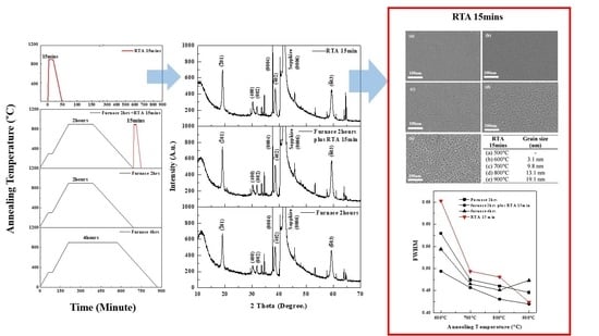
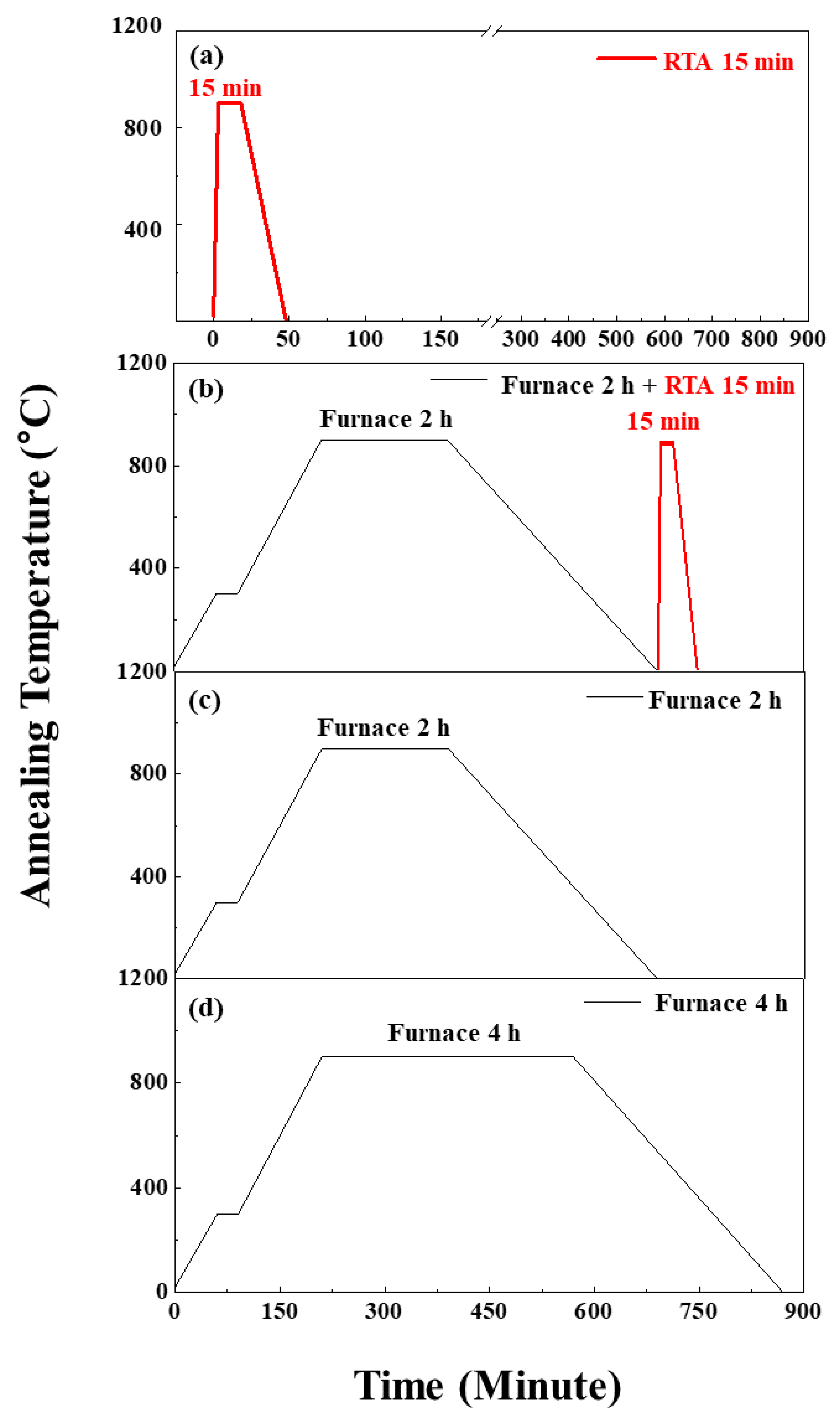
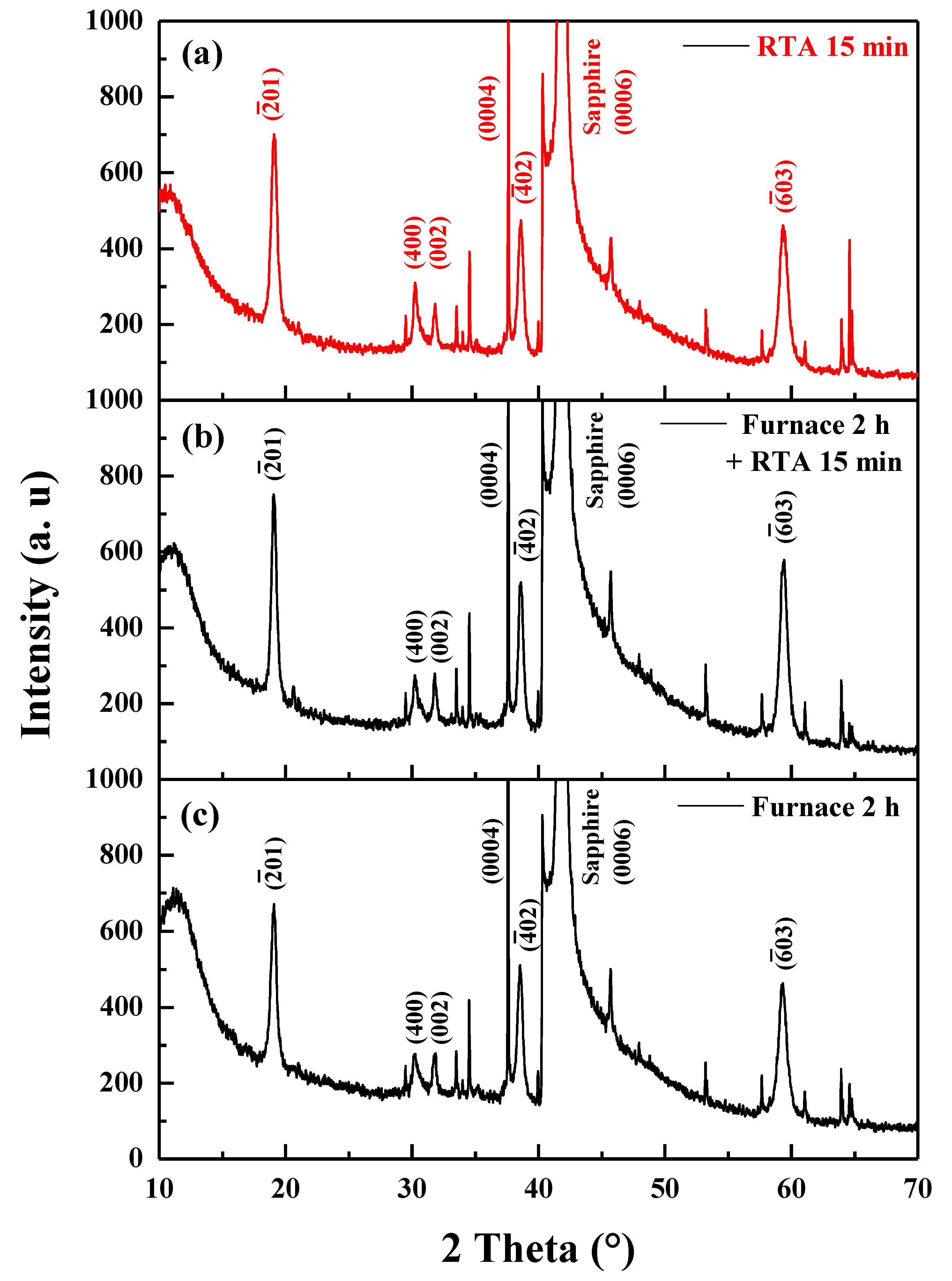
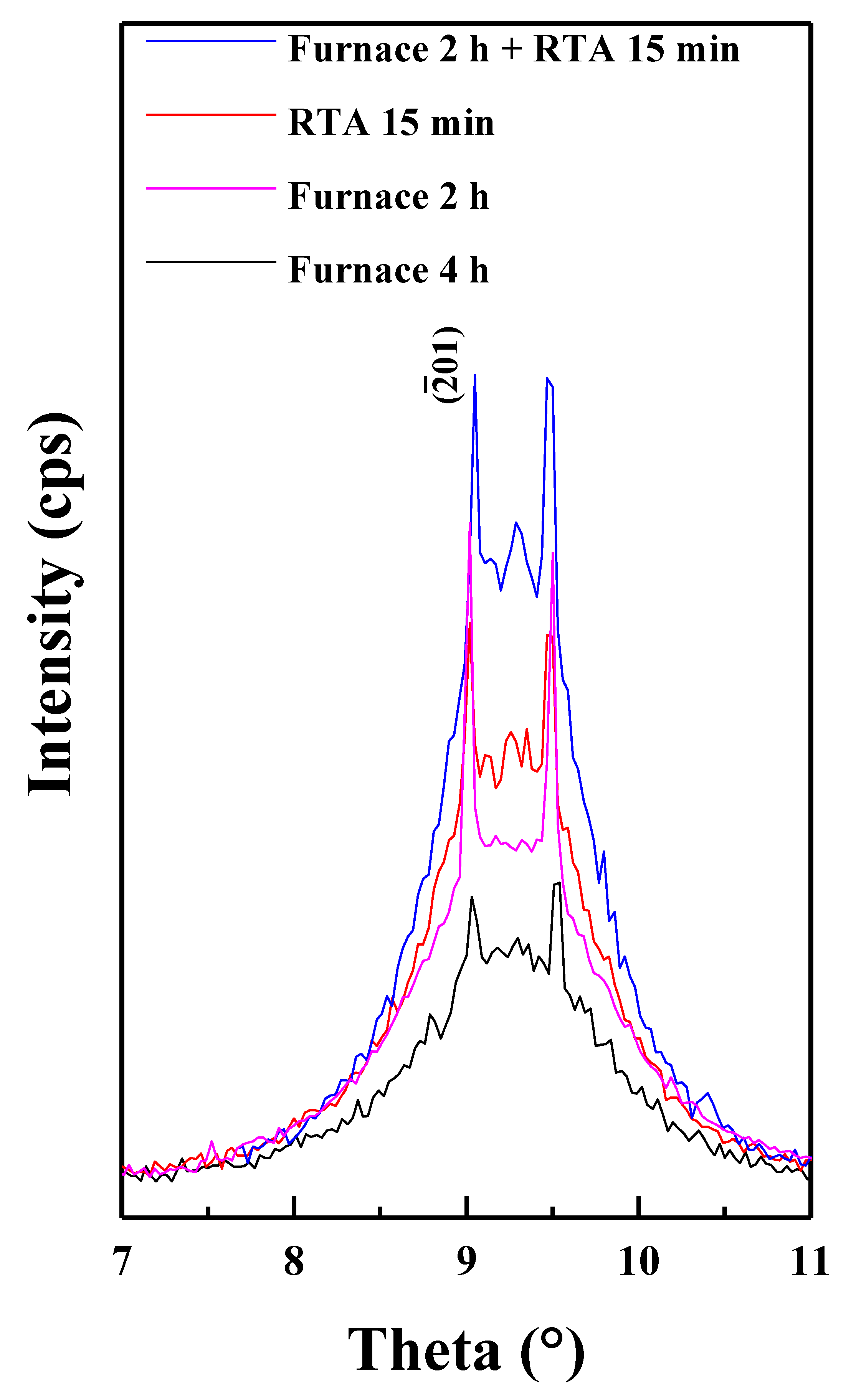
2.3. Annealing Method under Various Condition Using Electric Furnace and RTA Process

Spin coating using a solution and removing organic matter through curing of the hot plate process and annealing was carried out using an electric furnace and the RTA method. The sol–gel processed Ga2O3 thin films were annealed in the furnace for 2 and 4 h at 500–900 °C in oxygen atmosphere. As a comparative experiment, Ga2O3 thin films were annealed in a furnace for 2 h and sequentially annealed via the RTA process for 15 min. The temperature-heating rate of the furnace was set to increase by 5 °C/min, and the annealing process to remove the impurities was carried out for 2 and 4 h, respectively. The condition to raise the temperature of the RTA process was designed at 5 °C per second and maintained for 15 min at each temperature [21]. It is mentioned that the color of the substrate changes to green when the spin-coating and hot plate process are performed, but if β-Ga2O3 was obtained through annealing, the substrate changes transparently. We confirmed that these changing of colors are related with generation of β-Ga2O3 phase, and we could expect that β-Ga2O3 was formed by obtaining the same results even after the RTA process.

2.4. Thin Film Characterization

After the deposition process, the structure and qualitative measurement of the thin films were analyzed by X-ray diffraction (XRD) and high-resolution X-ray diffraction (HRXRD). First, we observed the structure analysis of the sample by X-ray diffraction (XRD, D8-Advance/Bruker-AXS, Karlsruhe, Germany). Based on the 2 theta (°) value, the process proceeded from 10 to 20 degrees., and the measurement time is 17 min. The wavelength of the X-ray is 0.154056 nm, and a Cu-Kα source was used. The β-Ga2O3 thin film quality and rocking curve was determined by high-resolution X-ray diffraction (HRXRD, D8-Discover/Bruker-AXS, Karlsruhe, Germany). It applied from 7 to 11 Theta (°). The wavelength of the X-ray is 0.154056 nm, and a Cu-Kα source was used. From the XRD result, sequential peaks of (−201), (−402), (−603), and (400), (002) were observed. This means that β-Ga2O3 thin films can be obtained by employing RTA and a high-temperature annealing process. Moreover, after increasing the annealing temperature range, the peak intensities were increased. We calculated the FWHM (full width at half maximum) from the main peak of (−201), and the crystallite size was found to be proportional to the annealing temperature using the Scherrer Equation (1) [22].
D =   0.89 × λ B × cos θ
where θ is the Bragg angle in radians, λ is the X-ray wavelength of the CuKα source of the XRD instrument, 0.89 is the constant, and B is FWHM value of the main peak in this experiment (−201) plane. Transmittance measurement and band-gap calculation were carried out to analyze the optical properties of β-Ga2O3 thin film. The transmittance spectra were obtained using the UV-vis spectrometer (Lambda 35, Perkin Elmer, Waltham, MA, USA). To measure the transmittance of β-Ga2O3 deposited on sapphire in orientation (0001), the analysis was conducted at a wavelength from 200 to 800 nm. Moreover, we employed alpha-step profiler to find thin film thickness to get the band gap. In order to extrapolate information about the energy band gap of β-Ga2O3, we derived it using from the Tauc Equation (2) [23].
α h v = C ( h v E g ) 1 / 2
where C is the optical constant, α is the coefficient, Eg is the optical bandgap, and is the photon energy. For thin film surface analysis, the characteristics could be measured using FE-SEM. Observe the surface morphology of the sample by field-emission scanning electron microscope (FE-SEM, SIGMA 300, Carl Zeiss, Jena, Germany). The ETH operating voltage was 5.00 kV, and signal A proceeded in In Lens mode and Magnification in 200.00 K. Furthermore, a comparative analysis of grain size obtained as a result of XRD and the thin film surface image was obtained through FE-SEM [24,25].

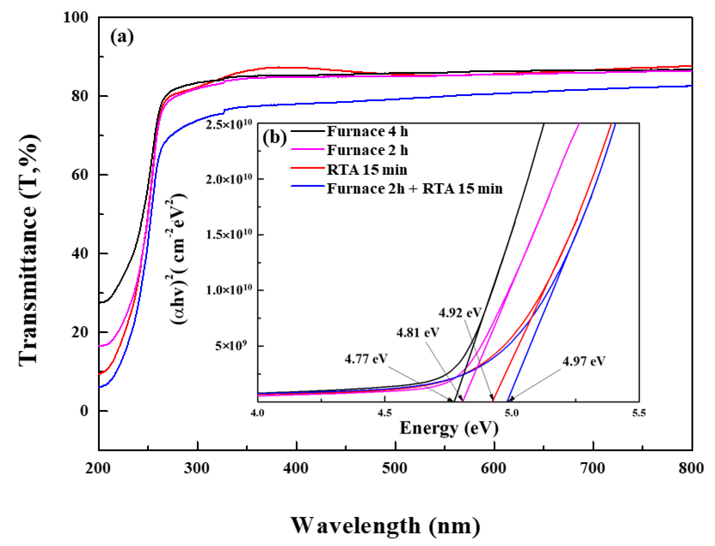
3. Results and Discussion

Figure 1 shows the schematic diagram of the β-Ga2O3 thin film annealing process employed in these experiments. We have conducted a comparative study of the thermal annealing process and optical annealing process by varying the annealing time in the furnace from 2 to 4 h, and the optical annealing process was applied to compare the annealing effects. To compare the annealing effects, a 2 and 4 h thermal annealing process, hybrid annealing process of 2 h thermal and 15 min optical energy, and optical annealing of 15 min process were employed. Before the RTA annealing process, to obtain the β-Ga2O3 thin film, a 2 h preheating process was performed at 900 °C. The RTA process was carried out very rapidly within 15 min. The furnace took about an hour to remove organic matter from the thin film surface at 300 degrees in one step. In addition, to reach 900 °C, which is the annealing temperature, it took 2 h to raise the temperature. In addition, it takes about 8 h to lower the temperature to room temperature to take out the sample. In the case of RTA, it takes about 2 min to reach 900 degrees, and it takes about 35 min, including 15 min for annealing process time and 15 min for taking out the sample at room temperature. It can be seen that RTA corresponds to 7.3% of the electric furnace process time and requires little energy in manufacturing thin films. Moreover, the amount of energy used to reach 900 °C is relatively small. Therefore, RTA is appropriate for a β-Ga2O3 thin film rapid process rather than a furnace.
Figure 2 displays the XRD pattern of the β-Ga2O3 thin film annealed by a thermal furnace at the various temperatures of 500, 600, 700, 800, and 900 °C. After the spin-coating and hot plate curing process, samples were annealed in the furnace under an oxygen ambient condition for 4 h. In general, Ga2O3 thin film can be crystalized at the high annealing temperature of 700 °C [15,26,27]. In our experiment, Ga2O3 thin film has an amorphous phase annealed at 500 °C, but it has a β-phase structure annealed at 600 °C. Moreover, after increasing the annealing temperature up to 800 °C, β-Ga2O3 thin film has a more highly oriented peak of (−201), while other minor peaks of (400) and (002) remained. However, at the annealing temperature of 900 °C, the main peak intensity of (−201) was slightly decreased, while other minor peaks of (400) and (002) were increased. The degradation of the main peak of (−201) probably comes from the thermal migration and diffusion process due to the high annealing temperature [28,29]. We believe that more high thermal energy than 700 °C is required to increase the (400), (002) peaks. Therefore, (400) and (002) remained stable during the 700 °C annealing process.
Figure 3 shows the XRD pattern of the β-Ga2O3 thin film, which performed annealing processes in the following conditions: furnace 2 h, furnace 2 h + RTA 15 min, and RTA 15 min at 900 °C, respectively. Comparing the specimens that annealed different conditions, the Ga2O3 thin film annealed at furnace 2 h + RTA 15 min showed the highest peak intensities of (−201), (−402), and (−603). We believe that this is due to the additional annealing process of RTA; during this process, Ga2O3 can have additional surface energy through post annealing. We can argue that the β-Ga2O3 thin film was formed by observing the peak of (−201). Thermal annealing of 900 °C or an additional optical annealing process can help to form the β-Ga2O3 thin film in the sapphire substrates. By comparing the XRD results of β-Ga2O3 thin film annealed at 2 h thermal annealing and thermal annealing with an optical annealing process, it can be seen that they have similar peak intensities and peak positions. It means there are no significant changes in the structural properties when the thermal appealing process was conducted at more than 900 °C.
Figure 4 shows the HRXRD rocking curve of the (−201) peak reflection by various annealing processes at 900 °C. β-Ga2O3 (−201) was obtained from 2θ at 19.07°. Thus, the measurement was carried out using HRXRD from 6° to 12°. As shown in the HRXRD results, it seems that the observed peaks were separated. Multiple peaks were observed by the rocking curves of the (−201) peak. We believe that these split multiples of the (−201) rocking curves probably come from the monoclinic phase of β-Ga2O3. Since β-Ga2O3 thin films were prepared by sol–gel and a spin-coating method, they did not have an epitaxial structure. However, by comparison of the FWHM value, we have confirmed that the β-Ga2O3 thin films have a crystalized phase with relatively high orientational structure properties. However, when comparing the tendency of the half width by the rocking curve of furnace 2 h and furnace 2 h + RTA 15 min, it was confirmed that the crystal growth was better in the (−201) direction when post annealing was applied.
Figure 5 shows the structural orientational tendency of each annealing processed specimen by considering the FWHM according to temperature. The (−201) peaks of FWHM were selected to compare the crystalline structure. From 600 to 800 °C, all four processes show the same tendency to decrease FWHM. At 700 °C, all processes were rapidly decreasing FWHM due to grain growth. Moreover, in the section where the temperature increased from 800 °C to 900 °C, as shown in the XRD result, it can be seen that the FWHM increases due to the reduced peak intensity of the furnace at 4 h. Since the furnace annealing processing was carried out for more than 4 h, we believe that a mosaic grain growth process happened. Therefore, the FWHM of the (−201) peaks increased. On the contrary, it can be seen that the FWHM of other specimens was reduced sharply due to the crystallization process of β-Ga2O3 thin films. By studying the FWHM according to various annealing process, it seems that the RTA method can be the most favorable post-annealing process to manufacture β-Ga2O3 thin films with high (−201) orientation.
Table 1 shows the experimental conditions for the FWHM and grain size of β-Ga2O3 based on the different annealing methods. Grain size was derived using a Scherrer formula with FWHM values. According to the results, it can be confirmed that the FWHM of the (−201) peaks in β-Ga2O3 decreases and the grain size increases as the annealing temperature gradually moves upward. Overall, the grain size of furnace 2 h + RTA 15 min was the largest compared to the conventional method furnace 2 h. Moreover, at 900 °C, the RTA performs a similar grain size to the other processes.
Figure 6 shows the FE-SEM images of β-Ga2O3 thin films prepared at (a) 500 °C, (b) 600 °C, (c) 700 °C, (d) 800 °C, and (e) 900 °C using different annealing methods: furnace 4 h and RTA (non-furnace). In the furnace 4 h process, we could see the tendency of the grain size to increase by up to 800 °C, but at 900 °C, we could see that the grain size became smaller as a result of excessive sintering. Whereas, in the case of RTA annealing without the furnace, as shown by the FE-SEM image, the grain size is increasing as the temperature rises. In addition, both annealing processes were identified as amorphous at 500 °C (Figure 6a), and the grain was gradually formed from 600 °C (Figure 6b). As a result, the β-phase was confirmed above 700 °C in both processes. In addition, the grain size increased as the temperature increased. In addition, when measuring the grain size, it was analyzed that the RTA and furnace processes were similar in size. It seems that increasing the annealing temperature can affect the grain growth more essentially. Therefore, RTA is an annealing process that can replace the furnace to form a β-Ga2O3 thin film.
Figure 7 shows the transmittance spectra and Tauc plots of β-Ga2O3 thin films prepared at 900 °C in various annealing processes: furnace 2 h, furnace 2 h + RTA 15 min, furnace 4 h, RTA 15 min. Depending on the various annealing processes, a transmittance measurement was performed on a β-Ga2O3 thin film deposited on a sapphire substrate within a wavelength range from 200 to 800 nm. As shown in Figure 7, the transmittance of each annealing process sample is presented as 82%, 80%, 78%, and 68% in terms of furnace 4 h, furnace 2 h, RTA 15 min, and furnace 2 h + RTA 15 min, respectively. The band gap of furnace 4 h, furnace 2 h, RTA 15 min, and furnace 2 h and RTA 15 min are presented as 4.77 eV, 4.81 eV, 4.92 eV, and 4.97 eV. These band-gap results were the same as the tendency of XRD, FE-SEM, and variation of FWHM according to the process method. Materials have their own properties and become more pronounced as the temperature increases. β-Ga2O3 is a material with a wide band gap of 4.8 eV and has insulator properties. Thus, similar to the XRD result with the highest peak intensity, the properties of the material were best revealed in furnace 2 h + RTA 15 min, which allowed for the analysis to have the largest band gap of 4.9 eV. If β-Ga2O3 is deposited with a sol–gel process through a furnace for 2 h, it can be confirmed that a typical band-gap result of 4.81 eV is obtained. Moreover, for the furnace 4 h process, the band gap is 4.77 eV, which is relatively small compared to the other processes. The reason for these results would be the effect of a long time of sintering at a high annealing temperature of 900 °C for 4 h, resulting in a defect increase in the grain caused by the diffusion of Al impurities from sapphire (Al2O3) substrate.

4. Conclusions

We proceeded with the annealing of furnace 4 h, furnace 2 h + RTA 15 min, and RTA 15 min processes (non-furnace) to compare with annealing to create a β-Ga2O3 thin film deposition. We were also able to analyze XRD, HRXRD transmittance, alpha-step, and Tauc plot, and found that the furnace 2 h + RTA 15 min process was more efficient compared to furnace 2 h, furnace 4 h, and RTA 15 min. In addition, it was found that the RTA process (non-furnace) was an overwhelmingly short process, and through the analysis of FWHM and grain size, which were obtained through rocking curves and XRD peak intensity, the crystallinity was also similar to the conventional furnace process annealed at the same temperature. As for the limitations of the proposed method, unlike a furnace, where multiple sample annealing processes are possible at a time, RTA can proceed with only one sample process. However, an eco-friendly and efficient RTA process that uses less energy can reduce the existing process time of β-Ga2O3 and provide more opportunities for wide band-gap material research.

Author Contributions

Data curation, M.-S.B. and J.-S.B.; formal analysis, M.-S.B. and J.-H.K.; investigation, M.-S.B., S.-H.K. and J.-S.B.; project administration, J.-H.K.; validation, M.-S.B.; writing—original draft M.-S.B. and S.-H.K.; writing—review and editing, M.-S.B. and J.-H.K. All authors have read and agreed to the published version of the manuscript.

Funding

This research was supported by the Chung-Ang University Research Grants in 2020 and by the Korea Institute of Energy Technology Evaluation and Planning (KETEP), the Ministry of Trade, Industry & Energy (MOTIE) of the Republic of Korea (No. 20214000000700).

Institutional Review Board Statement

Not applicable.

Informed Consent Statement

Not applicable.

Data Availability Statement

The data presented in this study are available on request from the corresponding author.

Acknowledgments

We are deeply thanks for Masaya Ichimura at Nagoya Institute of Technology for his kind guidance.

Conflicts of Interest

The authors declare no conflict of interest.

References

  1. Higashiwaki, M. Current status of Ga2O3 power devices. Appl. Phys. 2016, 55, 1202A1. [Google Scholar]
  2. Ajram, S.; Salmer, G. Ultrahigh frequency DC-to-DC converters using GaAs power switches. IEEE Trans. Power Electron. 2001, 16, 594–602. [Google Scholar] [CrossRef]
  3. Akasaki, H.; Amano, M.; Kito, K. Hiramatsu Photoluminescence of Mg-doped p-type GaN and electroluminescence of GaN p-n junction LED. J. Lumin. 1991, 48–49, 666–670. [Google Scholar] [CrossRef]
  4. Casady, J.B.; Johnson, R.W. Status of silicon carbide (SiC) as a wide-bandgap semiconductor for high-temperature applications: A review. Solid-State Electron. 1996, 39, 1409–1422. [Google Scholar] [CrossRef]
  5. Tsao, J.Y.; Chowdhury, S.; Hollis, M.A.; Jena, D.; Johnson, N.M.; Jones, K.A.; Kaplar, R.J.; Rajan, S.; Van de Walle, C.G.; Bellotti, E.; et al. Ultrawide-Bandgap Semiconductors: Research Opportunities and Challenges. Adv. Electron. Mater. 2018, 4, 1600501. [Google Scholar] [CrossRef] [Green Version]
  6. Zhang, H.; Yuan, L.; Tang, X.; Hu, J.; Sun, J.; Zhang, Y.; Zhang, Y.; Jia, R. Progress of Ultra-Wide Bandgap Ga2O3 Semiconductor Materials in Power MOSFETs. IEEE Trans. Power Electron. 2020, 35, 5157–5179. [Google Scholar] [CrossRef]
  7. Yoshioka, S.; Hayashi, H.; Kuwabara, A.; Oba, F.; Matsunaga, K.; Tanaka, I. Structures and energetics of Ga2O3 polymorphs. J. Phys. Condensed. Matter. 2007, 19, 346211. [Google Scholar] [CrossRef]
  8. Nikl, M. Wide band gap scintillation materials: Progress in the technology and material understanding. Phys. Stat. Sol. 2000, 178, 595. [Google Scholar] [CrossRef]
  9. Baliga, B.J. The future of power semiconductor device technology. Proc. IEEE 2001, 89, 822–832. [Google Scholar] [CrossRef]
  10. Rafique, S.; Han, L.; Tadjer, M.J.; Freitas, J.A., Jr.; Mahadik, N.A.; Zhao, H. Homo epitaxial growth of β-Ga2O3 thin films by low pressure chemical vapor deposition. Appl. Phys. Lett. 2016, 108, 182105. [Google Scholar] [CrossRef]
  11. Altuntas, H.; Donmez, I.; Ozgit-Akgun, C.; Biyikli, N. Electrical characteristics of β-Ga2O3 thin films grown by PEALD. J. Alloy. Compd. 2014, 593, 190–195. [Google Scholar] [CrossRef] [Green Version]
  12. Kumar Saikumar, A.; Nehate, S.D.; Sundaram, K.B. Review—RF Sputtered Films of Ga2O3. ECS J. Solid State Sci. Technol. 2019, 8, Q3064–Q3078. [Google Scholar] [CrossRef]
  13. Sasaki, K.; Higashiwaki, M.; Kuramata, A.; Masui, T.; Yamakoshi, S. MBE grown Ga2O3 and its power device applications. J. Cryst. Growth 2013, 378, 591–595. [Google Scholar] [CrossRef]
  14. Zhang, F.B.; Saito, K.; Tanaka, T.; Nishio, M.; Guo, Q.X. Structural and optical properties of Ga2O3 films on sapphire substrates by pulsed laser deposition. J. Cryst. Growth 2014, 387, 96–100. [Google Scholar] [CrossRef]
  15. Kokubun, Y.; Miura, K.; Endo, F.; Nakagomi, S. Sol-gel prepared β-Ga2O3 thin films for ultraviolet photodetectors. Appl. Phys. Lett. 2007, 90, 031912. [Google Scholar] [CrossRef]
  16. Xiang, Y.; Zhou, C.; Wang, W. Characterization of spin-coated gallium oxide films and application as surface passivation layer on silicon. J. Alloy. Compd. 2017, 699, 1192–1198. [Google Scholar] [CrossRef]
  17. Rafique, S.; Han, L.; Zhao, H. Thermal annealing effect on β-Ga2O3 thin film solar blind photodetector hetero epitaxially grown on sapphire substrate. Phys. Status Solidi A 2017, 214, 1700063. [Google Scholar] [CrossRef]
  18. Kang, H.S.; Kang, J.S.; Kim, J.W.; Lee, S.Y. Annealing effect on the property of ultraviolet and green emissions of ZnO thin films. J. Appl. Phys. 2004, 95, 1246. [Google Scholar] [CrossRef]
  19. Wang, J.; Ye, L.; Wang, X.; Zhang, H.; Li, L.; Kong, C.; Li, W. High transmittance β-Ga2O3 thin films deposited by magnetron sputtering and post-annealing for solar-blind ultraviolet photodetector. J. Alloy. Compd. 2019, 803, 9–15. [Google Scholar] [CrossRef]
  20. Dong, L.; Jia, R.; Xin, B. Effects of post-annealing temperature and oxygen concentration during sputtering on the structural and optical properties of β-Ga2O3 films. J. Vac. Sci. Technol. 2016, A34, 060602. [Google Scholar] [CrossRef]
  21. Jo, G.H.; Koh, J.H. Laser annealing effects on Ga dopants for ZnO thin films for transparent conducting oxide applications. Ceram. Int. 2019, 45, 6190–6197. [Google Scholar] [CrossRef]
  22. Holzwarth, U.; Gibson, N. The Scherrer equation versus the ‘Debye-Scherrer equation’. Nat. Nanotech. 2011, 6, 534. [Google Scholar] [CrossRef] [PubMed]
  23. Sangiorgi, N.; Aversa, L.; Tatti, R.; Verucchi, R.; Sanson, A. Spectrophotometric method for optical band gap and electronic transitions determination of semiconductor materials. Opt. Mater. 2017, 64, 18–25. [Google Scholar] [CrossRef]
  24. Țălu, Ș. Micro and Nanoscale Characterization of Three Dimensional Surfaces. Basics and Applications; Napoca Star Publishing House: Cluj-Napoca, Romania, 2015; pp. 21–27. [Google Scholar]
  25. Țălu, Ș.; Kulesza, S.; Bramowicz, M.; Stepien, K.; Dastan, D. Analysis of the Surface Microtexture of Sputtered Indium Tin Oxide Thin Films. Arch. Metall. Mater. 2021, 66, 443–450. [Google Scholar]
  26. Ghose, S.; Rahman, S.; Hong, L.; Rojas-Ramirez, J.S.; Jin, H.B.; Park, K.B.; Klie, R.; Droopad, R. Growth and characterization of β-Ga2O3 thin films by molecular beam epitaxy for deep-UV photodetectors. J. Appl. Phys. 2017, 122, 095302. [Google Scholar] [CrossRef]
  27. Pearton, S.J.; Yang, J.; Cary, P.H., IV; Ren, F.; Kim, J.H.; Tadjer, M.J.; Mastro, M.A. A review of Ga2O3 materials, processing, and devices. Appl. Phys. Rev. 2018, 5, 011301. [Google Scholar] [CrossRef] [Green Version]
  28. Krishnamurthy, G.V.; Chirumamilla, M.; Rout, S.S.; Furlan, K.P.; Krekeler, T.; Ritter, M.; Becker, H.-W.; Yu Petrov, A.; Eich, M.; Störmer, M. Structural degradation of tungsten sandwiched in hafnia layers determined by in-situ XRD up to 1520 °C. Sci. Rep. 2021, 11, 3330. [Google Scholar] [CrossRef]
  29. Wu, X.; Bek, A.; Bittner, A.M.; Eggs, C.; Ossadnik, C.; Veprek, S. The effect of annealing conditions on the red photoluminescence of nanocrystalline Si/SiO films. Thin Solid Films 2003, 425, 175–184. [Google Scholar] [CrossRef]
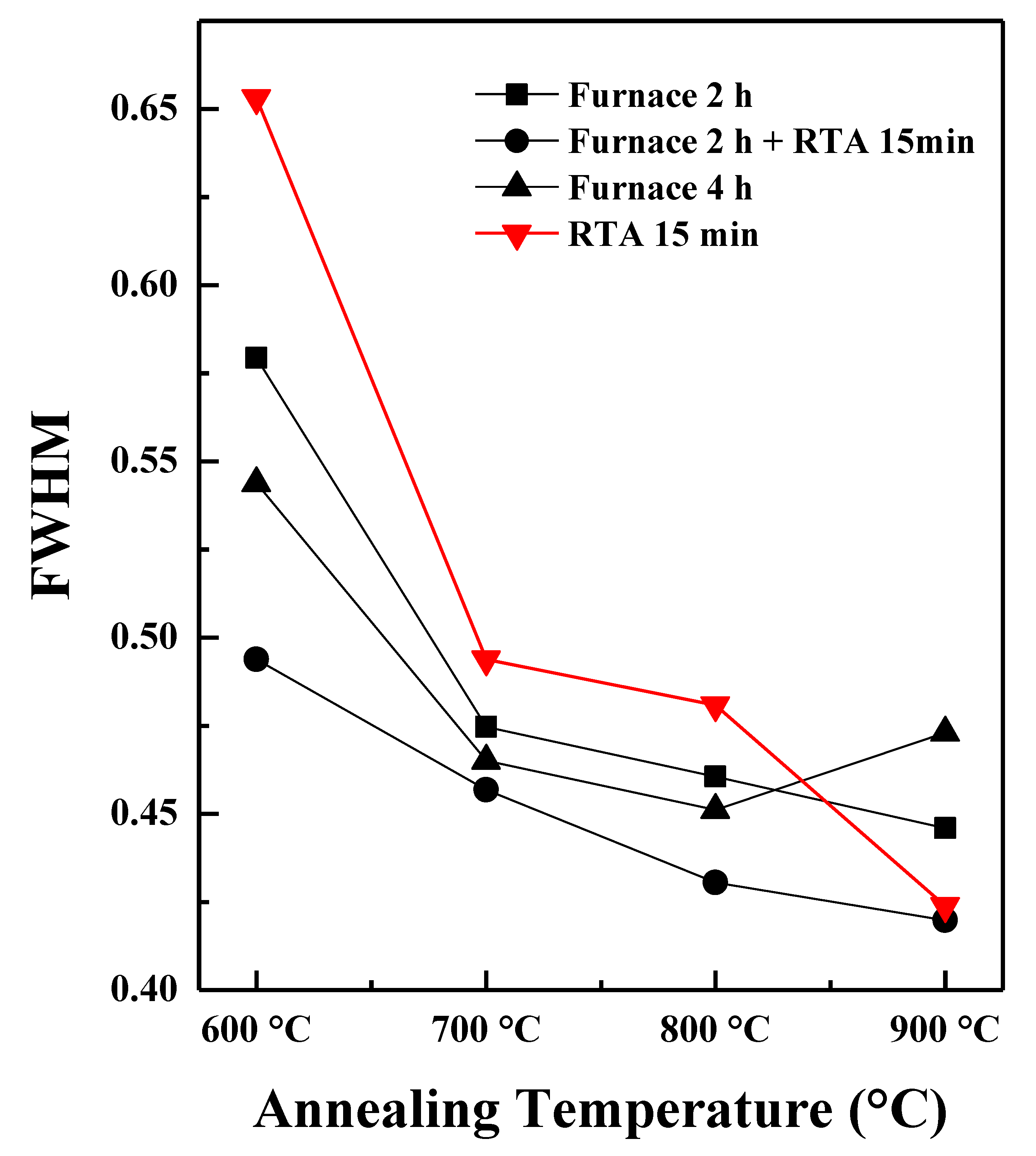
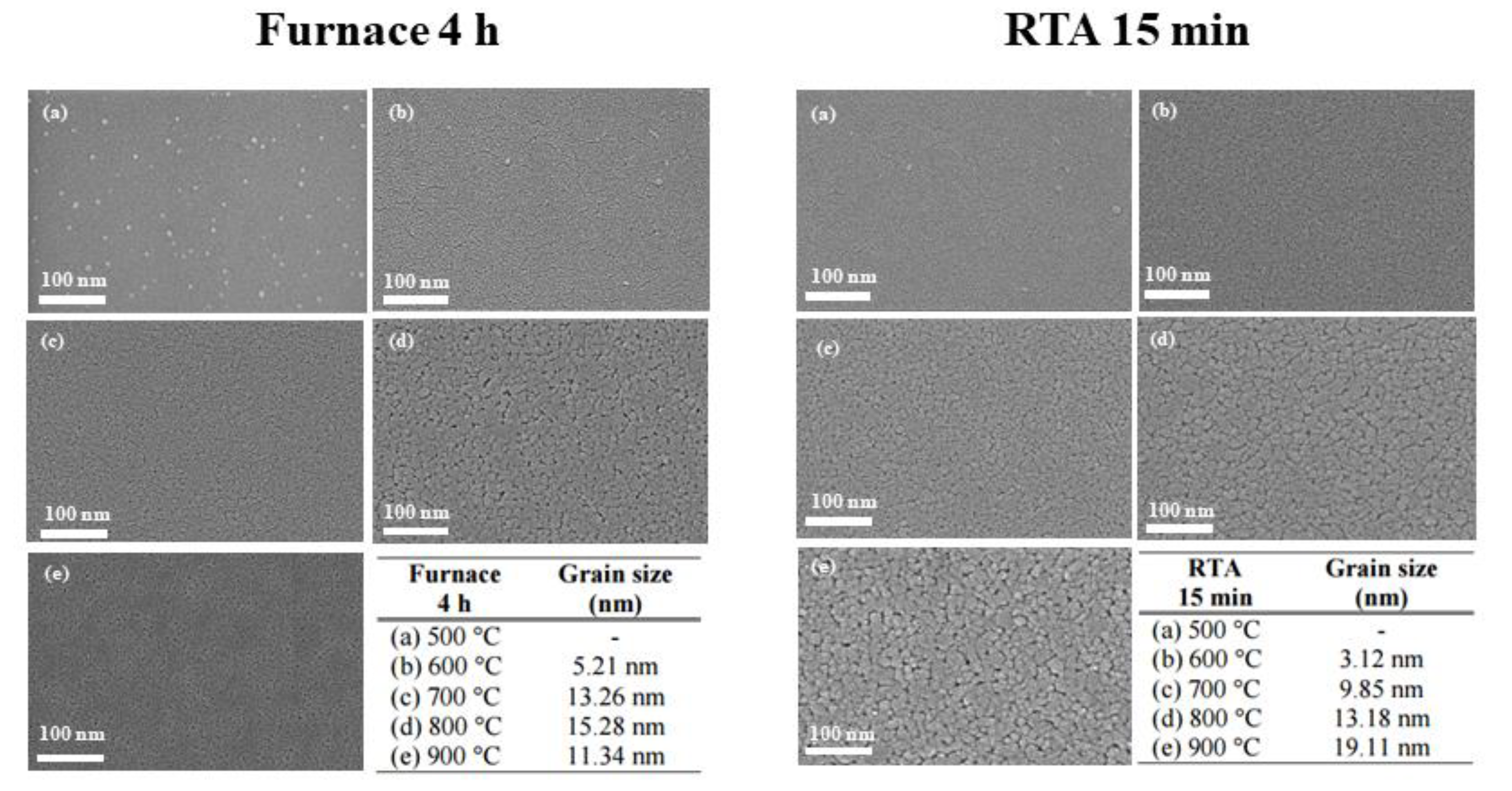
Figure 1. Schematic diagram of β-Ga2O3 thin film annealing method applied with various processes. (a) RTA 15 min, (b) furnace 2 h + RTA 15 min, (c) furnace 2 h, (d) furnace 4 h.
Coatings 11 01220 g001
Figure 2. X-ray diffraction patterns of post-annealed β-Ga2O3 thin films with various temperature ranges from 500 to 900 °C in the furnace.
Coatings 11 01220 g002
Figure 3. X-ray diffraction patterns of β-Ga2O3 thin films proceeded at various annealing methods: (a)—RTA 15 min at 900 °C, (b)—furnace 2 h + RTA 15 min, and (c)—furnace 2 h.
Coatings 11 01220 g003
Figure 4. X-ray rocking curve of the super lattice for (−201) reflection in various annealing processes.
Coatings 11 01220 g004
Figure 5. Results of FWHM and grain size by various annealing processes and temperatures.
Coatings 11 01220 g005
Figure 6. FE-SEM images of β-Ga2O3 thin films prepared via furnace and RTA processes: (a)—500 °C, (b)—600 °C, (c)—700 °C, (d)—800 °C, and (e)—900 °C using different annealing methods: furnace 4 h and RTA (non-furnace). Magnification: 200.00 K X; Acceleration voltage: 5.00 kV; Working distance: 4.8 mm. Image resolution pixel: 1024 × 768 pixel.
Coatings 11 01220 g006
Figure 7. (a) Transmittance spectra and (b) Tauc plots of β-Ga2O3 thin films prepared at 900°C in various annealing processes: furnace 2 h, furnace 2 h + RTA 15 min, furnace 4 h, RTA 15 min.
Coatings 11 01220 g007
Table 1. FWHM and grain size of β-Ga2O3 based on the different annealing methods.
Annealing MethodSampleFWHMGrain Size (nm)
Furnace 2 h600 °C0.5814.5
700 °C0.4717.7
800 °C0.4618.3
900 °C0.4518.9
Furnace 2 h
+ RTA 15 min
600 °C0.4917.1
700 °C0.4618.4
800 °C0.4319.5
900 °C0.4220.2
Furnace 4 h600 °C0.5415.5
700 °C0.4618.1
800 °C0.4518.6
900 °C0.4717.8
RTA 15 min600 °C0.6512.9
700 °C0.4917.1
800 °C0.4817.5
900 °C0.4219.9
Publisher’s Note: MDPI stays neutral with regard to jurisdictional claims in published maps and institutional affiliations.

