Article

Study on the Electrical, Structural, Chemical and Optical Properties of PVD Ta(N) Films Deposited with Different N2 Flow Rates

1
Department of Microelectronics, North China University of Technology, Beijing 100144, China
2
Department of Physics, Dhaka University of Engineering & Technology, Gazipur 1707, Bangladesh
3
High-Tech Innovation Institute, North China University of Technology, Beijing 100144, China
4
Research and Education Center “Technological Center”, MIREA—Russian Technological University, 119454 Moscow, Russia
*
Authors to whom correspondence should be addressed.
Coatings 2021, 11(8), 937; https://doi.org/10.3390/coatings11080937
Submission received: 4 July 2021 / Revised: 29 July 2021 / Accepted: 29 July 2021 / Published: 5 August 2021

Abstract

:
By reactive DC magnetron sputtering from a pure Ta target onto silicon substrates, Ta(N) films were prepared with different N2 flow rates of 0, 12, 17, 25, 38, and 58 sccm. The effects of N2 flow rate on the electrical properties, crystal structure, elemental composition, and optical properties of Ta(N) were studied. These properties were characterized by the four-probe method, X-ray diffraction (XRD), X-ray photoelectron spectroscopy (XPS), and spectroscopic ellipsometry (SE). Results show that the deposition rate decreases with an increase of N2 flows. Furthermore, as resistivity increases, the crystal size decreases, the crystal structure transitions from β-Ta to TaN(111), and finally becomes the N-rich phase Ta3N5(130, 040). Studying the optical properties, it is found that there are differences in the refractive index (n) and extinction coefficient (k) of Ta(N) with different thicknesses and different N2 flow rates, depending on the crystal size and crystal phase structure.

1. Introduction

Transition metal nitrides, especially tantalum nitride (TaN), are in high demand for a wide range of applications due to their high melting point, hardness, excellent wear and corrosion resistance, refractory character, mechanical and high-temperature stability, chemical inertness, and histocompatibility [1,2,3,4,5,6]. Some prominent examples of such applications are as a protective coating material against oxidation and corrosion [7], as a diffusion barrier for Al and Cu metallization in advanced microelectronics [8,9,10,11], in phosphide and nitride optoelectronics as ohmic contact [3,4], in artificial heart valves as histocompatibility materials [12], thin film resistors [13], as ceramic pressure sensors [14], and also different mechanical applications [5,6]. The large interest for TaN arises since it is considered recently as a high thermal conductive material in microelectronic chips for the θ-TaN phase [15].
Furthermore, TaN belongs to the class of complex nitride phases of compounds which can vary from stoichiometry due to lattice vacancies. Diversifications in phase structure are common in TaN, from hexagonal-Ta2N, cubic-TaN, hexagonal-TaN, hexagonal-Ta5N6, tetragonal-Ta4N5, and orthorhombic-Ta3N5 including TaN, which led to large differences in physical, chemical, and mechanical properties. The TaN alloy forms a variety of phases depending on the deposition technique and growth conditions [16,17]. Numerous reports have been published to characterize sputtered TaN films based on various sputtering parameters such as nitrogen (N2) partial pressure ratio [18,19], N2/Ar flow rate ratio [20,21,22], sputtering power [23], and substrate temperature [24] during deposition. By controlling these different parameters, their influence on the structural, chemical, electrical, and optical properties of the TaN film have been investigated.
Among them, there are quite a few studies on how the N2 flow or N2/Ar flow rate ratio and the N2/(N2 + Ar) partial pressure ratio affect the properties of TaN film. Chen et al. [25] used a magnetron sputtering low-power radio frequency deposition method with variable nitrogen flow rate to deposit TaNx barrier layers on silicon. They found that as the N2 flow rate increases, the surface roughness of the deposited TaNx film is slightly increased, and the amorphous structure of TaNx is formed with good thermal stability. Zaman et al. [26] prepared a TaN film with a 3% to 25% N2/(N2 + Ar) ratio on Si substrate by reactive magnetron sputtering and studied the effect of N2 partial pressure on the crystal structure and hardness of the TaN film. It was found that the deposited films with 5% and 3% N2 content show the highest hardness (33 Pa).
Although sputtered TaN films have been widely investigated for their different properties, their optical properties have not yet been analyzed as much. Recent studies show that spectroscopic ellipsometry (SE) can be used to characterize and measure thin film thickness because of its fast and non-destructive nature [2,27,28,29]. Aouadi et al. [2] have studied the effects of varying N2 flow rates from 1 to 4 sccm on the structural and optical properties of TaN thin films. They report that the optical constants (ε1, ε2) may be used in conjunction with real-time SE to monitor and control the growth of tantalum nitride films. Cherfi et al. [30] deposited TaN films with an N2 flow rate of 0–12 sccm on Si (100) and glass substrates by DC magnetron sputtering to show the influence of nitrogen flow on the crystal structure and optical properties of TaN. It was shown that for low N2 flow (1 and 2 sccm), the TaN films show good conductor performance; a further increase of N2 flow shows non-metallic behavior. At the same time, samples with similar structural properties have similar behaviors in terms of optical properties. Waechtler et al. show that SE can be used to examine the optical properties of Ta and TaN thin films from 75 to 380 nm thickness. They found a good agreement of optical properties with narrow-band data available for similar thin films. It was also shown that the optical properties of the films strongly depend on both substrate and film thickness [27]. Ma et al. studied the temperature-dependent dielectric function of TiN films by SE [28]. Recently, Xu et al. [31] used the method of comparing the measured the refractive index of low-k film under the Ta(N) diffusion barrier with the refractive index of the blank low-k film to study the integrity of the Ta(N) diffusion barrier using the approach developed by Shamiryan et al. [32]. The abbreviation Ta(N), used hereinafter, refers to the complex films containing both Ta and TaN with different nitrogen concentrations. The Ta/TaN stacks are used, for instance, as metal diffusion barriers in advanced microelectronics.
However, there has been limited study of the optical behavior of the different stoichiometries of thicker TaN films by SE with varying N2 flow rates in conjunction with electronic, structural, and chemical composition. The study of the optical properties of TaN can provide us with more information about TaN films and some potential possibilities for the development of new applications. Thus, the systematic study of TaN films for understanding the electrical, structural, chemical composition, and optical properties are required.
Therefore, we first focused our attention on the optical properties of TaN films by SE, a non-destructive testing method. By examining the optical properties of the sample, it can provide some guidance for the deposited sample. However, past studies did not focus on the influence of process conditions on either the refractive index (n) or extinction coefficient (k), which are important optical parameters for Ta and TaN films because n and k are regarded as “fingerprints of thin film materials”. Then, the effects of deposition rate and N2 flow on the deposition of Ta(N) films on the electrical, structural, and optical properties (n & k), as well as the elemental composition, of TaN films were studied by using the four-probe method, X-ray diffraction (XRD), and X-ray photoelectron spectroscopy. The observation of different phases and chemical composition evaluation observed by XRD, XPS were correlated with optical properties.

2. Materials and Methods

Ta(N) films were synthesized using a standard magnetron sputtering (JS35-80G) system. The Ta(N) films were deposited on Si (100) wafers using magnetron sputtering of a Ta target (8.0 cm in diameter and 6.0 mm thick) of 99.95% purity. The substrate holder (located in the center of the chamber) was a 25 cm diameter plate, with rotation set to 10 rpm without heating the substrate for all of the depositions to improve the uniformity of the films. The target-to-substrate distance was 13.0 cm, and a negative bias was applied to the Ta target. After placing the Si (100) substrate in the deposition chamber, the chamber was evacuated to 9.6 × 10⁻⁴ Pa (by a turbo-molecular pump, Beijing Taiyueheng Vacuum Technology Research Institute, Beijing, China), the background vacuum was sufficient to ensure the vacuum required for Ta(N) film sputtering. Ar (99.999% purity) and N2 (99.999% purity) were introduced into the reaction chamber through a mass flow controller (Beijing Qixing Huachuang Electronics Co., Ltd., Beijing, China) and used as sputtering and reaction gases, respectively. The Ta target and the Si-substrate were sputter cleaned with Ar plasma before the Ta(N) films deposition for 5 min. Following cleaning, Ta(N) film was deposited at 9.56 × 10⁻⁴ Pa background pressure and 200 W DC power was applied in a mixture of Ar and N2.
To study the influence of different N2 flow rates on the properties of the sputtered Ta(N) film, in all sputtering processes, the flow rate of Ar was fixed at 58 sccm with various N2 flow rates from 0 to 58 sccm. The ratio of the reactive gas (N2, 0–58 sccm) to the sputter gas (argon, 58 sccm) were varied from 0 to 0.20, 0.29, 0.43, 0.65, and 1.00. The deposition time was also varied from 10 to 30 min to study whether the thickness of the film affects the optical properties, among other properties, of Ta(N) under each N2 flow rate. However, when the N2 flow was 12 and 17 sccm, the sputtering process commenced for only 10 min.
The thickness of the film was measured by a German Bruker Dektak step meter (Berlin, Germany). The resolution of the Dektak profilometer was 4 angstroms. The thickness was determined from the step height between the film and a masked substrate area. The resistivity of the sample was measured by a double-electric four-point resistance resistivity tester (FT-341) and was obtained from the current between two external probes and by measuring the voltage through the internal probes.
The crystallographic structure of the sputtered Ta(N) films was measured by an X-ray diffractometer (Rigaku Ultima IV, Tokyo, Japan) using a θ–2θ scan with a 1.54 Å wavelength Cu Kα radiation, at room temperature, working at 40 kV and 30 mA, which recorded the diffraction intensity in the scattering angle range of 20°–60°.
X-ray photoelectron spectroscopy (XPS) was used to investigate the elemental composition and chemical states in Ta(N) films using PHI 5300 (PerkinElmer, Fremont, CA, USA) with an Mg Kα (1253.6 eV) excitation source. This source was operated using a voltage of 12.5 kV and an emission current of 20 mA. The films were sputter cleaned in an Ar+ environment with 89.45 eV pass energy for 5 min prior to measurement. Survey scans were conducted in the 0–1100 eV range.
The optical characterization of the films was carried out using a SENpro spectroscopic ellipsometer (SENTECH, Berlin, Germany) to measure phase (Δ) and amplitude ratio (Ψ) changes in the reflected light. The incident angle was fixed at 70° in the spectral range from 400 to 1050 at 5 nm increments. In all cases, the ellipsometric data were processed using SpectraRay/3 software (SpectraRay/3 V2022-125) for the data analysis. By treating the Ψ−∆ spectra, the refractive index (n) and extinction coefficient (k) of the corresponding Ta(N) films were extracted by using E. Kondoh ELLIPSHEET [33] for an infinitely thick film. The validity of this approach is proved below in the ellipsometry part of this paper. The specific details and film thicknesses are given in Table 1.

3. Results and Discussion

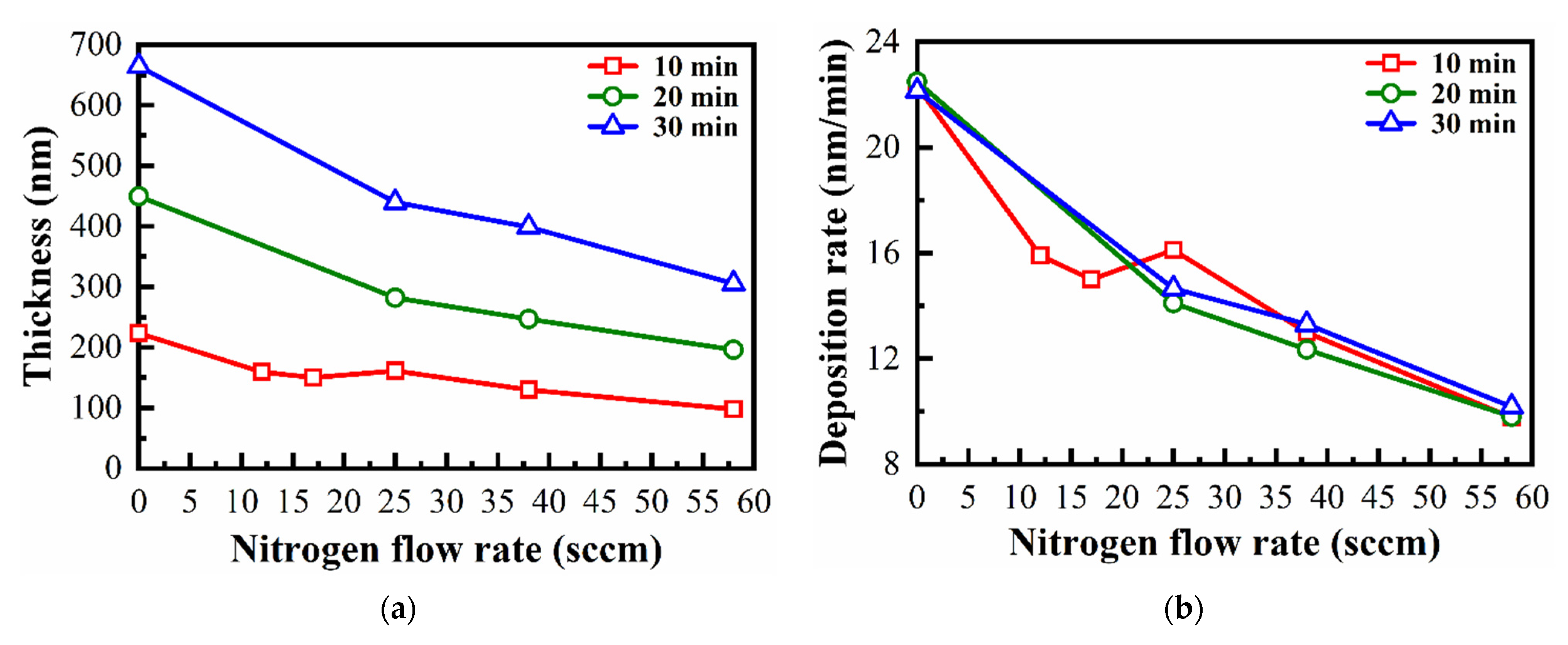
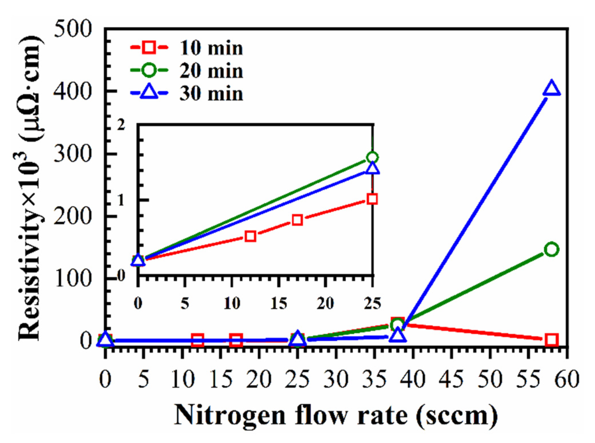
3.1. Deposition Rate and Resistivity

The deposition rate of Ta(N) films, sheet resistance, and resistivity depend on the flow of nitrogen. The film thickness decreases with an increasing flow of nitrogen, as shown in Figure 1a. The increase of sputtering time from 10 to 30 min makes the film thicker. However, the deposition rate does not depend on the sputtering time (Figure 1b). With the increase of nitrogen flow in the sputtering atmosphere of ionized Ar+, the intensity of ion bombardment of the Ta target decreases due to the reduction of the mean free path length. The number of sputtered Ta atoms also decreases, leading to a gradual reduction in deposition rate [34]. In addition, since there are a large number of active N atoms in the sputtering atmosphere (an increase of the N2 flow rate), the number of active N atoms in the atmosphere gradually increases, which increases the chemical reaction between active N atoms and the surface of the Ta target. There is a possibility of the TaN compound causing a slight poisoning of the target [35,36] and thereby reducing the sputtering rate.
The electrical resistivity of pure Ta films sputtered for 10, 20, and 30 min are nearly the same (193.5, 197.4, and 193.9 µΩ·cm, respectively (Table 1)). It is interesting to notice that the measured resistivity for pure Ta films is similar to the values reported for tetragonal crystalline Ta (β-Ta) films (165 µΩ·cm, Schauer et al. [37]; 210 µΩ·cm, Cuong et al. [38]) and 242 µΩ·cm, Arshi et al. [39]). Therefore, our pure Ta films are most likely β-Ta. The electrical resistivity of Ta(N) films deposited with different nitrogen flows is shown in Figure 2. It can be seen that the resistivity of TaN is higher than the resistivity of pure Ta observed at zero nitrogen flow. The introduction of nitrogen increases resistivity, changing linearly (embedded graph), with the thinner film offering lower resistivity. The trend of increased resistivity can be attributed to the decreasing of the low resistivity Ta phase in the deposited Ta-N films and the increasing of the low resistivity N-rich TaN phase. A much more dramatic change of resistivity is observed in the films deposited with 58 sccm N2 flow, especially after 30 min deposition (relatively thick films, see Table 1).
Further increase of N2 flow increases the resistivity of Ta(N) film and may depend on the formation of different surface topographies, grain sizes, changes of composition, amorphous structure formations, and defects/imperfections (scattering from grain boundary) [40]. The resistivity of TaN films in the current work is similar to the values reported in the literature [40,41]. When the N2 flow rate is 12 sccm, the resistivity of the sputtered TaN film is increased to 524 µΩ·cm and close to FCC TaN [42,43,44,45], or cubic TaN(111) [39], or Ta3N5, or Ta5N6 [46,47,48]. After a further increase in the nitrogen flow to 25 sccm, the resistivity of the sputtered TaN film is close to the resistivity of Ta3N5 (1126 µΩ·cm, [39]). Remarkably, when the increase of N2 flow is increased to 38 and 58 sccm, the resistivity of the sputtered TaN films drastically increases, with the only exception being the 10 min deposition TaN films. Normally, this can be explained by increasing electron scattering from interstitial N atoms. [39]. However, this model does not explain so strong a difference between the films deposited with 38 and 58 sccm [49]. It is also well-known that an excess of N2 flow rate will decrease the mean free path of ionized Ta atoms, disturb the formation of TaN structures [40,50], and also increase electron scattering from interstitial N atoms. Therefore, the phase of the TaN film generated under our N2 flow rate will also be different. The existence of N-rich phases in the TaN films at higher nitrogen flows is consistent with both the XRD patterns and the XPS analysis.

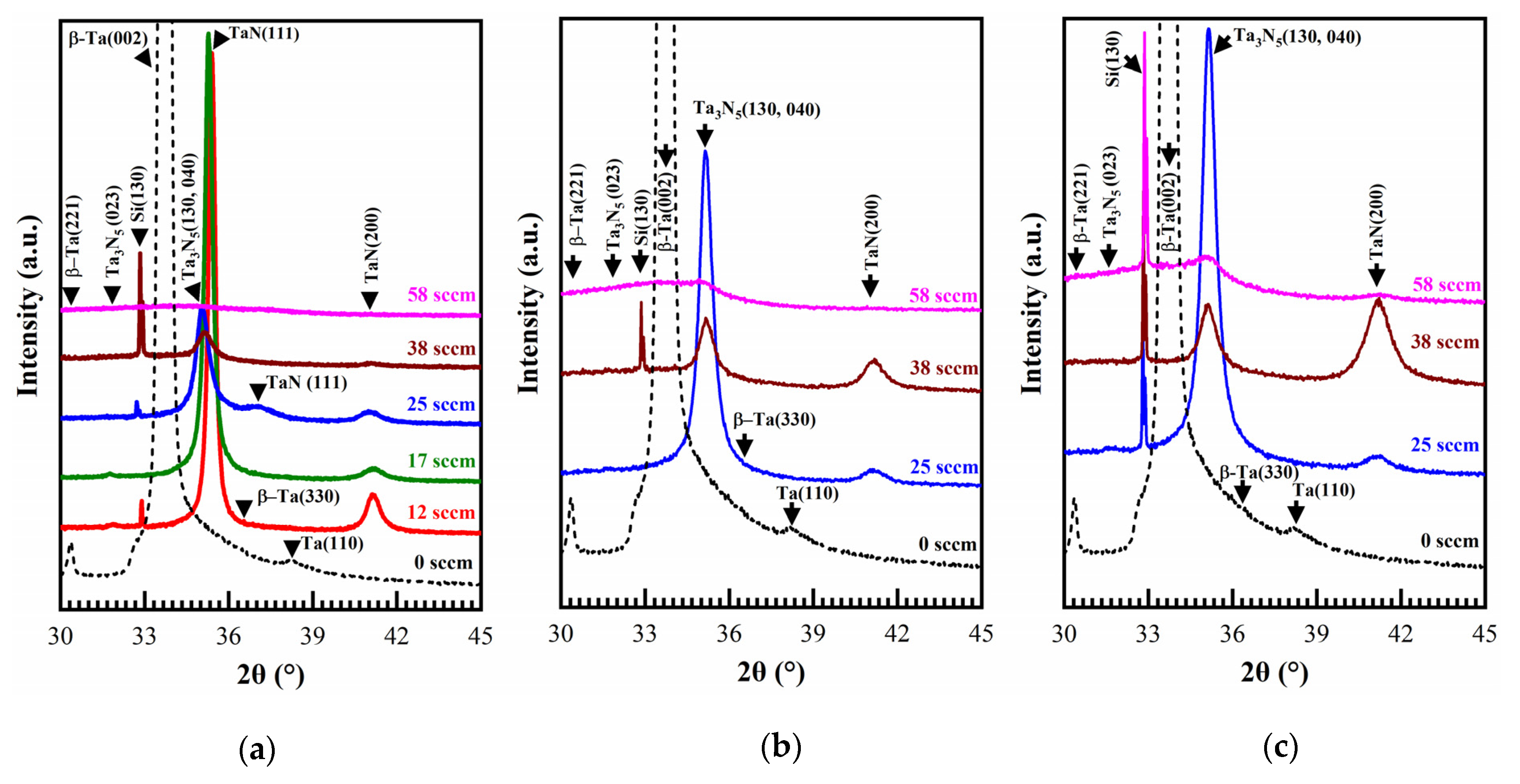
3.2. Structural Properties (XRD Analysis)

Figure 3 shows the X-ray diffraction (XRD) patterns of the Ta(N) films deposited for 10, 20, and 30 min with different N2 flows in the gas mixture varying from 0 to 58 sccm. The XRD spectra of the Ta films (N2 flow rate is 0) shows a mixed phase of β-Ta (221), β-Ta (002), β-Ta (330), and Ta (110). The diffraction intensity of (002) is the highest, and the peak area of the diffraction peak is the largest, which indicates that the Ta film that was sputtered is mainly β-Ta (002) preferred orientation (PDF#: 04-0788). Peaks at 35.40°, 37.04°, and 41.20° are indexed to be the TaN (111), TaN (111) [39], and TaN (200) (PDF#: 49-1283) structures respectively (Figure 3a). The peaks at 31.86°, and 35.10° correspond to Ta3N5 (123) and Ta3N5 (130) or (040) compounds respectively [51].
When the N2 flow rate is 12 and 17 sccm, a mixed phase of TaN (111) and TaN (200) appears, and the diffraction peak of Ta3N5 (023) also appears when the N2 flow rate is 17 sccm. However, the diffraction peak of TaN (111) is the highest, and the diffraction peak area is also the largest, which indicates that the preferred orientation of the TaN film under these two flow rates is TaN (111). Similarly, when the N2 flow rate is 38 and 58 sccm, the TaN film has a preferred orientation of Ta3N5 (130,040). At the same time, when the N2 flow rate increases, the diffraction peaks gradually widen, indicating that the grain size is gradually decreasing, leading to high resistivity (Table 1). Correspondingly, this could be attributed to the mixture of fcc TaN and its amorphous structure [46,52,53]. These phenomena observed by XRD are in line with our previous conjectures in the section on resistivity and are similar to those reported in an earlier study [43,44].
When the nitrogen flow rate is increased, the phase of the film evolves gradually from TaN (111) to Ta3N5 (130), or Ta3N5 (040) (35.40° to 35.03°) [51]. Furthermore, the TaN (200) peaks are gradually decreasing. A broad peak corresponding to Ta3N5 appears for the 58 sccm sample and significant broadening of the peaks may be due to the formation of a two-phase nanocomposite structure. This may be attributed to the high nitrogen fraction, which is known to inhibit the crystallization of nitrogen-rich TaNx sputtered films. At the same time, the XRD patterns of TaN films with a nitrogen flow rate of 25–58 sccm and a sputtering time of 10–30 min were compared (Figure 3b,c), and it was found that the XRD patterns of TaN films with the same nitrogen flow rate but different sputtering times/different thicknesses did not change much, showing that the thickness of the film does not affect the formation of the crystal structure of the film. Generally, the films deposited with 58 sccm of nitrogen do not have pronounced patterns and this suggests that the films are losing their crystalline structure and becoming more amorphous (Table 2). The full width at half maximum (FWHM) was obtained by Gaussian fitting and corresponding crystallite size was calculated by a Debye–Scherrer equation (D = 0.9λ/βcosθ), where D is the crystal size, λ is the wavelength of X-ray, θ is the Braggs angle in radians, and β is the FWHM of the peak in radians. For each peak of XRD spectra one sample was used. The crystallite sizes presented in Table 2 are obtained from Figure 3a samples.

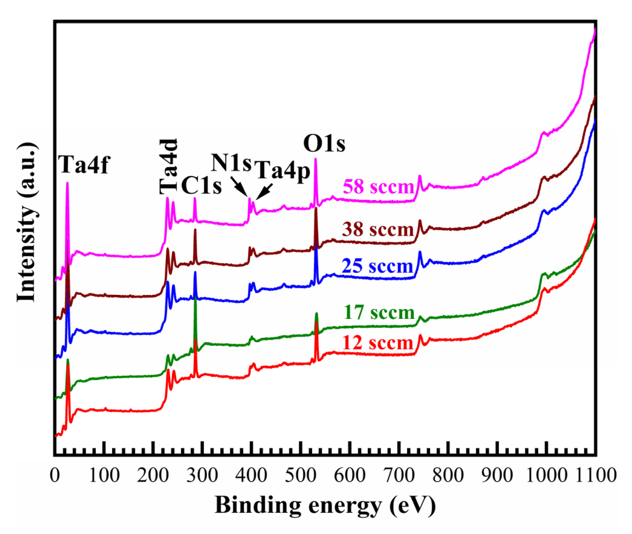
3.3. Elemental Composition (XPS Studies)

XPS spectra were obtained to ascertain the elemental composition of the deposited TaN films. Figure 4 illustrates an evolution of the XPS survey spectrum of the deposited TaN films as a function of N2 flow rate in the binding energy range of 0–1150 eV and show the Ta, O, N, and C signals. It is confirmed that the survey does not contain additional components that arise in the Si2p spectrum because our films were thicker. The O and C signal in these spectra might come from the ambient atmosphere and/or the presence of background oxygen in the sputtering chamber during sputtering, and/or from organic residues during the storage, as already reported in the literature [35,39,53], which may vary depending on the different sputtering instruments used. There is a chemical shift for both O and C in the lower binding energy with an increase in the N2 flow rates due to the formation of Ta2O5 (Figure 5a,b). It can be assumed that the most probable origin of these residues is associated with impurities present in the nitrogen and/or a decrease in the Ta sputtering rate, which increases the effect of residual gases.
The XPS core-level spectra of Ta4f, Ta4d, and N1s for different N2 flow rates (12–58 sccm) are shown in Figure 6a–c, respectively. Figure 6a shows the XPS region of Ta4f, revealing that it is composed of three overlaying bonding environments: Ta4f5/2 of Ta-Ox (Ta bonded with O), Ta4f7/2,5/2 of Ta-N, and Ta4f7/2 of Ta-N located at 30.25, 28.15, and 25.97 eV, respectively. As shown in Figure 6a, increasing the flow of N2 from 12 to 58 sccm is likely to chemically shift the Ta4f7/2 peaks from 25.97 to 25.78 eV, which were attributed to TaN Ta4f5/2 peaks. Furthermore, the chemical shift from 30.25 to 29.81 reveals that O-rich films composed of Ta2O5 with an increase of N2 flows were observed.
Figure 7 shows the deconvoluted spectra of Ta4f for the TaN films with an N2 flow of 12 sccm. Compared with the referred Ta binding energy values of TaN and TaOx, the binding energy values in the Ta4f spectrum (Ta4f7/2 = 25.7 eV and Ta4f5/2 = 27.7 eV) accorded with the chemical state of Ta in Ta–O binding [54]. The Ta4f doublet at binding energy Ta4f7/2 = 27.3 eV and Ta4f5/2 = 29.0 eV matched Ta5+ state in Ta2O5 [55,56], while the corresponding Ta4f doublet peaks are located respectively at Ta4f7/2 = ~25.1 eV and Ta4f5/2 = ~27.3 eV that should be attributed to N-rich TaN phase [57,58]. The existence of the Ta–N bonding in the film is further confirmed by the N1s peak located around 397.0 eV [59]. As the nitrogen flow rate increases, more Ta–N bonds form and the N 1s peak also increases. This is consistent with the XRD spectra. It can be seen from Figure 6c that the N1s peak shifts from 397.55 to 398.85 eV for nitrogen flow from 12 to 58 sccm, while the Ta4p3/2 peak also shifts from 406.4 to 404.95 eV. It is noteworthy that there are uncertainties on the exact value for Ta4p binding energy. Nyholm et al. reported a Ta4p value of 400.9 eV [60] and Tian et al. [61] reported a relatively high value of 406.0 eV. This shift in the binding energy for the N1s peaks toward lower values are in agreement with a previous study [35,39], while the binding energies for the Ta4f doublets also shift toward lower energy values and do not agree with previous studies.

3.4. Optical Properties

Spectroscopy ellipsometry (SE) is broadly used as an important tool for thin films thickness, refractive indices and optical properties analysis, and its basic principle is shown elsewhere [62]. In this study, the films were optically thick and the measured Ψ and Δ of all Ta films and TaN films were used for direct calculation of optical characteristics by using the substrate model. The n and k values of the corresponding film were obtained by using E. Kondoh ELLIPSHEET [33]. For each curve (n and k) of SE, one sample was used for the calculation.
Figure 8a,b depict the complex refractive index (n) and extinction coefficient (k), respectively for Ta films and with a comparison with the literature report. After comparing with the data of Tompkins et al. [63]. and Waechtler et al. [27], it is found that the changing trends of n and k of Ta films with different thicknesses are roughly the same, and the thickness does have an effect on the optical properties of Ta films. This is different to Waechtler et al., who reported the same n, k of Ta films with different thicknesses.
In Figure 9, we compare the refractive index (n) and extinction coefficient (k) of our sputtered TaN film with an N2 flow rate of 12–58 sccm with the data of Aouadi et al. [2] and Waechtler et al. [27]. Also, it is found that when the N2 flow rate is 12 and 17 sccm, the n and k of our sputtered TaN film are close to the values in the reference. However, as the N2 flow rate increases, the n and k values of our sputtered TaN film become further from the n and k values in the references (Figure 9a,b). Furthermore, different N2 flow rates and different thicknesses of TaN films have significant differences in n and k, which shows that both N2 flow rate and thickness affect the optical properties of TaN. In addition, we can see that there are differences in the n and k values and curve shapes of TaN films with different crystal structures. The influence of N2 flow rate on the n and k of TaN film may be caused by the different crystal structures and grain sizes of TaN film deposited with different N2 flow rates. It is interesting that the extinction coefficient of TaN films deposited at high nitrogen flows (38 and 58 sccm) decreases starting from 700 nm and especially from 900 nm. The reduction of the extinction coefficient suggests that the films are becoming more dielectric-like and explains the drastic increase of their resistivity (Figure 2).
In this work, we used optically thick films to extract optical characteristics. The thicknesses of these films are measured by using a Bruker Dektak step meter that is used only for relatively thick film. However, many applications of Ta and TaN layers need very low thickness. For instance, when they are used as diffusion barriers in advanced microelectronics. Taking this into account, we examined the applicability of ellipsometry to measure the thickness of the thin Ta and TaN layers. For this purpose, we used the values of the optical characteristics of these layers found in literature and measured in our work. Then we calculated Δ–Ψ trajectories for the films with different thicknesses (Figure 10). The presented curves demonstrate that Ta(N) film thickness can be measured by ellipsometry when d ≤ 100 nm. The sensitivity is reduced with thickness, but it can be very good for evaluation of Ta(N) films deposited as diffusion barriers for microelectronics application (d < 10 nm). It is also apparent that ellipsometry may be efficient for evaluation of d < 100 nm films, as it was in [31,32].

4. Conclusions

The Ta(N) film with different N2 flow rates (0–58 sccm) and sputtering times of 10–30 min was deposited by the DC reactive magnetron sputtering method, and it was found that the Ta(N) film deposition rate, electrical, structural, chemical and optical properties depend on N2 flow rate. As the N2 flow rate increases from 0 to 58 sccm, the crystal structure of the sputtered film transitions from β-Ta to TaN (111) and finally becomes the N-rich phase Ta3N5 (130) or Ta3N5 (040). When the N2 flow rate increases, the diffraction peaks gradually widen, which indicates that the grain size is decreasing, leading to higher resistivity (Table 1), and so correspondingly could be attributed to the mixture of fcc TaN and its amorphous structure The films deposited with 58 sccm of nitrogen lose specific crystallographic patterns and therefore become amorphous. In studying the optical properties, we can see that both the thickness and the N2 flow rate affect the refractive index (n) and extinction coefficient (k) of TaN film, and have a greater impact on k. The curve shapes of n and k of similar crystal structures have a small difference. The influence of N2 flow rate on the refractive index and extinction coefficient of TaN film may be caused by the different crystal structures and grain size of TaN film deposited with different N2 flow rates. The extinction coefficient of the films deposited with 58 sccm of nitrogen decreases, which suggests the formation of a more dielectric-like nature of the deposited films. This fact explains the drastic increase in the resistivity of the films shown in Figure 2. The reason for the transformation to the dielectric state is the incorporation of Ta oxide that can be seen from XPS data. When the nitrogen flow is so large, it reduces the free path length of sputtered atoms, poisons the Ta target and therefore reduces the effective deposition rate. As a result, the role of the residual oxygen is drastically increased and the deposited film becomes tantalum oxynitride with much higher resistivity. This effect becomes more pronounced when the deposition time is longer, which is the reason for the strong difference in resistivity between the films deposited during 10 and 30 min. If deposition time is short, the target poisoning might be negligible.
Finally, the presented results suggest the resistivity of TaN films deposited by magnetron sputtering can be precisely controlled by changing nitrogen concentration during deposition. It is also important to note that too high a concentration of nitrogen may have the negative effect of increasing the impact of gas phase impurities.

Author Contributions

Conceptualization, M.R.B.; methodology, Y.H. and M.R.; validation, J.Z., J.Y., and M.R.B.; formal analysis, Y.H., M.R., Y.W., J.Z., J.Y., and M.R.B.; resources, Y.W., J.Z., and J.Y.; data curation, Y.H. and M.R.; writing—original draft preparation, Y.H. and M.R.; writing—review and editing, Y.H., M.R., and M.R.B.; visualization, Y.H. and M.R.; supervision, Y.W., J.Z., J.Y., and M.R.B.; funding acquisition, J.Z., J.Y., and M.R.B. All authors have read and agreed to the published version of the manuscript.

Funding

This research was funded by the National Natural Science Foundation of China (NSFC), Grant No. 61874002 and Russian Foundation for Basic Research (RFBR), Grant No. 18-29-27022. The APC was funded by NSFC, Grant No. 61874002.

Institutional Review Board Statement

Not applicable.

Informed Consent Statement

Not applicable.

Data Availability Statement

Not applicable.

Acknowledgments

We would like to express sincere thanks to Eiichi Kondoh from University of Yamanashi, Japan for his help to calculate the n and k from Δ and Ψ.

Conflicts of Interest

The authors declare no conflict of interest.

References

  1. Han, J.H.; Kim, H.Y.; Lee, S.C.; Kim, D.H.; Park, B.K.; Park, J.-S.; Jeon, D.J.; Chung, T.-M.; Kim, C.G. Growth of tantalum nitride film as a Cu diffusion barrier by plasma-enhanced atomic layer deposition from bis((2-(dimethylamino)ethyl) (methyl)amido)methyl(tert-butylimido)tantalum complex. Appl. Surf. Sci. 2016, 362, 176–181. [Google Scholar] [CrossRef]
  2. Aouadi, S.M.; Debessai, M. Optical properties of tantalum nitride films fabricated using reactive unbalanced magnetron sputtering. J. Vac. Sci. Technol. A Vac. Surf. Film 2004, 22, 1975–1979. [Google Scholar] [CrossRef]
  3. Kang, S.M.; Yoon, S.G.; Suh, S.J.; Yoon, D.H. Control of electrical resistivity of TaN thin films by reactive sputtering for embedded passive resistors. Thin Solid Films 2008, 516, 3568–3571. [Google Scholar] [CrossRef]
  4. Lovejoy, M.L.; Patrizi, G.A.; Roger, D.J.; Barbour, J.C. Thin-film tantalum-nitride resistor technology for phosphide-based optoelectronics. Thin Solid Films 1996, 290–291, 513–517. [Google Scholar] [CrossRef]
  5. Shin, C.-S.; Kim, Y.-W.; Hellgren, N.; Gall, D.; Petrov, I.; Greene, J.E. Epitaxial growth of metastable δ-TaN layers on MgO(001) using low-energy, high-flux ion irradiation during ultrahigh vacuum reactive magnetron sputtering. J. Vac. Sci. Technol. A Vac. Surf. Film 2002, 20, 2007. [Google Scholar] [CrossRef] [Green Version]
  6. Shin, C.-S.; Gall, D.; Kim, Y.-W.; Hellgren, N.; Petrov, I.; Greene, J.E. Development of preferred orientation in polycrystalline NaCl-structure δ-TaN layers grown by reactive magnetron sputtering: Role of low-energy ion surface interactions. J. Appl. Phys. 2002, 92, 5084–5093. [Google Scholar] [CrossRef]
  7. Patel, A.; Gladczuk, L.; Paur, C.S.; Sosnowski, M. Tantalum Nitride Seed Layers for Bcc Tantalum Coatings Deposited on Steel by Magnetron Sputtering. MRS Proc. 2002, 750, 523. [Google Scholar] [CrossRef]
  8. Dalili, N.; Liu, Q.; Ivey, D.G. Thermal and electrical stability of TaNx diffusion barriers for Cu metallization. J. Mater. Sci. 2013, 48, 489–501. [Google Scholar] [CrossRef]
  9. Volpi, F.; Cadix, L.; Berthomé, G.; Coindeau, S.; Encinas, T.; Jourdan, N.; Blanquet, E. Impact of silica-substrate chemistry on tantalum nitride thin films deposited by atomic layer deposition: Microstructure, chemistry and electrical behaviors. Thin Solid Films 2019, 669, 392–398. [Google Scholar] [CrossRef]
  10. Liu, C.H.; Liu, W.; Wang, Y.H.; Wang, Y.; An, Z.; Song, Z.X.; Xu, K.W. Interface stability and microstructure of an ultrathin α-Ta/graded Ta(N)/TaN multilayer diffusion barrier. Microelectron. Eng. 2012, 98, 80–84. [Google Scholar] [CrossRef]
  11. Witt, C.; Yeap, K.B.; Lesniewska, A.; Wan, D.; Jordan, N.; Ciofi, I.; Wu, C.; Tokei, Z. Testing The Limits of TaN Barrier Scaling. In Proceedings of the 2018 IEEE International Interconnect Technology Conference (IITC), Santa Clara, CA, USA, 4–7 June 2018; pp. 54–56. [Google Scholar]
  12. Leng, Y.; Sun, H.; Yang, P.; Chen, J.; Wang, J.; Wan, G.; Huang, N.; Tian, X.; Wang, L.; Chu, P. Biomedical properties of tantalum nitride films synthesized by reactive magnetron sputtering. Thin Solid Films 2001, 398–399, 471–475. [Google Scholar] [CrossRef]
  13. Shostachenko, S.A.; Zakharchenko, R.V.; Ryzhuk, R.V.; Leshchev, S.V. Thermal stability of tantalum nitride based thin film resistors. IOP Conf. Ser. Mater. Sci. Eng. 2019, 498, 012014. [Google Scholar] [CrossRef]
  14. Ayerdi, I.; Castaño, E.; García-Alonso, A.; Gracia, J. High-temperature ceramic pressure sensor. Sens. Actuators A Phys. 1997, 60, 72–75. [Google Scholar] [CrossRef]
  15. Kundu, A.; Yang, X.; Ma, J.; Feng, T.; Carrete, J.; Ruan, X.; Madsen, G.K.H.; Li, W. Ultrahigh Thermal Conductivity of θ-Phase Tantalum Nitride. Phys. Rev. Lett. 2021, 126, 115901. [Google Scholar] [CrossRef] [PubMed]
  16. Aouadi, S.M. Structural and mechanical properties of TaZrN films: Experimental and ab initio studies. J. Appl. Phys. 2006, 99, 053507. [Google Scholar] [CrossRef] [Green Version]
  17. Aouadi, S.M.; Bohnhoff, A.; Amriou, T.; Williams, M.; Hilfiker, J.N.; Singh, N.; Woollam, J.A. Vacuum ultra-violet spectroscopic ellipsometry study of single- and multi-phase nitride protective films. J. Phys. Condens. Matter 2006, 18, S1691–S1701. [Google Scholar] [CrossRef]
  18. Nazon, J.; Sarradin, J.; Flaud, V.; Tedenac, J.C.; Fréty, N. Effects of processing parameters on the properties of tantalum nitride thin films deposited by reactive sputtering. J. Alloys Compd. 2008, 464, 526–531. [Google Scholar] [CrossRef]
  19. Tsukimoto, S.; Moriyama, M.; Murakami, M. Microstructure of amorphous tantalum nitride thin films. Thin Solid Films 2004, 460, 222–226. [Google Scholar] [CrossRef]
  20. Bernoulli, D.; Müller, U.; Schwarzenberger, M.; Hauert, R.; Spolenak, R. Magnetron sputter deposited tantalum and tantalum nitride thin films: An analysis of phase, hardness and composition. Thin Solid Films 2013, 548, 157–161. [Google Scholar] [CrossRef]
  21. Lee, W.-H.; Lin, J.-C.; Lee, C. Characterization of tantalum nitride films deposited by reactive sputtering of Ta in N2/Ar gas mixtures. Mater. Chem. Phys. 2001, 68, 266–271. [Google Scholar] [CrossRef]
  22. Wang, J.H.; Chen, L.J.; Lu, Z.C.; Hsiung, C.S.; Hsieh, W.Y.; Yew, T.R. Ta and Ta–N diffusion barriers sputtered with various N2/Ar ratios for Cu metallization. J. Vac. Sci. Technol. B Microelectron. Nanom. Struct. 2002, 20, 1522. [Google Scholar] [CrossRef]
  23. Lee, T.; Watson, K.; Fen, C.; Gill, J.; Harmon, D.; Sullivan, T.; Li, B. Characterization and reliability of TaN thin film resistors. In Proceedings of the 2004 IEEE International Reliability Physics Symposium, Phoenix, AZ, USA, 25–29 April 2004; pp. 502–508. [Google Scholar]
  24. Hantehzadeh, M.R.; Mortazavi, S.H.; Faryadras, S.; Ghoranneviss, M. The effect of temperature on the structure of tantalum nitride (TaN) thin films deposited by DC plasma. J. Fusion Energy 2012, 31, 84–88. [Google Scholar] [CrossRef]
  25. Chen, S.-F.; Wang, S.-J.; Yang, T.-H.; Yang, Z.-D.; Bor, H.-Y.; Wei, C.-N. Effect of nitrogen flow rate on TaN diffusion barrier layer deposited between a Cu layer and a Si-based substrate. Ceram. Int. 2017, 43, 12505–12510. [Google Scholar] [CrossRef]
  26. Zaman, A.; Meletis, E. Microstructure and Mechanical Properties of TaN Thin Films Prepared by Reactive Magnetron Sputtering. Coatings 2017, 7, 209. [Google Scholar] [CrossRef] [Green Version]
  27. Waechtler, T.; Gruska, B.; Zimmermann, S.; Schulz, S.; Gessner, T. Characterization of Sputtered Ta and TaN Films by Spectroscopic Ellipsometry. In Proceedings of the 2006 8th International Conference on Solid-State and Integrated Circuit Technology, Shanghai, China, 23–26 October 2006; pp. 2184–2186. [Google Scholar]
  28. Ma, Q.; Shi, X.; Bi, L.; Li, J.; Zhou, Q.; Zhu, B. Influence of the deposition temperature on the optical and electrical properties of TiN film by spectroscopic ellipsometry. Superlattices Microstruct. 2021, 151, 106815. [Google Scholar] [CrossRef]
  29. Johs, B.D.; Hale, J.; Ianno, N.J.; Herzinger, C.M.; Tiwald, T.E.; Woollam, J.A. Recent developments in spectroscopic ellipsometry for in situ applications. In Optical Metrology Roadmap for the Semiconductor, Optical, and Data Storage Industries II.; Duparre, A., Singh, B., Eds.; International Society for Optics and Photonics: Bellingham, WA, USA, 2001; Volume 4449, pp. 41–57. [Google Scholar]
  30. Cherfi, D.E.; Guemmaz, M.; Bourahli, M.E.H.; Ouadfel, M.A.; Maabed, S. Effects of Nitrogen Flow Rate on the Structural, Morphological and Optical Properties of TaN Thin Films Grown by the DC Magnetron Sputtered Technique. Acta Phys. Pol. A 2019, 136, 849–854. [Google Scholar] [CrossRef]
  31. Xu, H.; Hu, Z.-J.; Qu, X.-P.; Wan, H.; Yan, S.-S.; Li, M.; Chen, S.-M.; Zhao, Y.-H.; Zhang, J.; Baklanov, M.R. Effect of thickness scaling on the permeability and thermal stability of Ta(N) diffusion barrier. Appl. Surf. Sci. 2019, 498, 143887. [Google Scholar] [CrossRef]
  32. Shamiryan, D.; Baklanov, M.R.; Maex, K. Diffusion barrier integrity evaluation by ellipsometric porosimetry. J. Vac. Sci. Technol. B Microelectron. Nanom. Struct. 2003, 21, 220. [Google Scholar] [CrossRef]
  33. Kondoh, E. Ellipsheet: Spreadsheet Ellipsometry (Excel Ellipsometer). Available online: http://www.ccn.yamanashi.ac.jp/~kondoh/ellips.html (accessed on 1 January 2021).
  34. Lee, K.; Lee, K. Optical Properties and X-ray Photoelectron Spectroscopy Study ofReactive-sputtered Ta-N Thin Films. J. Korean Phys. Soc. 2009, 55, 966–970. [Google Scholar] [CrossRef]
  35. Arshi, N.; Lu, J.; Joo, Y.K.; Yoon, J.H.; Koo, B.H. Effects of nitrogen composition on the resistivity of reactively sputtered TaN thin films. Surf. Interface Anal. 2015, 47, 154–160. [Google Scholar] [CrossRef]
  36. Cheviot, M.; Gouné, M.; Poulon-Quintin, A. Monitoring tantalum nitride thin film structure by reactive RF magnetron sputtering: Influence of processing parameters. Surf. Coatings Technol. 2015, 284, 192–197. [Google Scholar] [CrossRef]
  37. Schauer, A.; Roschy, M.R.F. sputtered β-tantalum and b.c.c. tantalum films. Thin Solid Films 1972, 12, 313–317. [Google Scholar] [CrossRef]
  38. Cuong, N.D.; Kim, D.-J.; Kang, B.-D.; Kim, C.S.; Yu, K.-M.; Yoon, S.-G. Characterization of Tantalum Nitride Thin Films Deposited on SiO2/Si Substrates Using dc Magnetron Sputtering for Thin Film Resistors. J. Electrochem. Soc. 2006, 153, G164. [Google Scholar] [CrossRef]
  39. Arshi, N.; Lu, J.; Lee, C.G.; Koo, B.H.; Ahmed, F. Effects of Nitrogen Content on the Phase and Resistivity of TaN Thin Films Deposited by Electron Beam Evaporation. JOM 2014, 66, 1893–1899. [Google Scholar] [CrossRef]
  40. Rossnagel, S.M. Characteristics of ultrathin Ta and TaN films. J. Vac. Sci. Technol. B Microelectron. Nanom. Struct. 2002, 20, 2328. [Google Scholar] [CrossRef]
  41. Lu, Y.; Weng, R.; Hwang, W.; Yang, Y. Study of phase transition and electrical resistivity of tantalum nitride films prepared by DC magnetron sputtering with OES detection system. Thin Solid Films 2001, 398–399, 356–360. [Google Scholar] [CrossRef]
  42. Oku, T.; Kawakami, E.; Uekubo, M.; Takahiro, K.; Yamaguchi, S.; Murakami, M. Diffusion barrier property of TaN between Si and Cu. Appl. Surf. Sci. 1996, 99, 265–272. [Google Scholar] [CrossRef]
  43. Willmott, D.J. Effect of nitrogen on the electrical and structural properties of triode-sputtered tantalum films. J. Appl. Phys. 1972, 43, 4865–4871. [Google Scholar] [CrossRef]
  44. Nie, H.B.; Xu, S.Y.; Wang, S.J.; You, L.P.; Yang, Z.; Ong, C.K.; Li, J.; Liew, T.Y.F. Structural and electrical properties of tantalum nitride thin films fabricated by using reactive radio-frequency magnetron sputtering. Appl. Phys. A Mater. Sci. Process. 2001, 73, 229–236. [Google Scholar] [CrossRef] [Green Version]
  45. Riekkinen, T.; Molarius, J.; Laurila, T.; Nurmela, A.; Suni, I.; Kivilahti, J. Reactive sputter deposition and properties of TaxN thin films. Microelectron. Eng. 2002, 64, 289–297. [Google Scholar] [CrossRef]
  46. Sun, X.; Kolawa, E.; Chen, J.-S.; Reid, J.S.; Nicolet, M.-A. Properties of reactively sputter-deposited Ta–N thin films. Thin Solid Films 1993, 236, 347–351. [Google Scholar] [CrossRef]
  47. Stampfl, C.; Freeman, A.J. Stable and metastable structures of the multiphase tantalum nitride system. Phys. Rev. B 2005, 71, 024111. [Google Scholar] [CrossRef] [Green Version]
  48. Ishikawa, A.; Takata, T.; Matsumura, T.; Kondo, J.N.; Hara, M.; Kobayashi, H.; Domen, K. Oxysulfides Ln2Ti2S2O5 as Stable Photocatalysts for Water Oxidation and Reduction under Visible-Light Irradiation. J. Phys. Chem. B 2004, 108, 2637–2642. [Google Scholar] [CrossRef]
  49. Fang, Z.; Aspinall, H.C.; Odedra, R.; Potter, R.J. Atomic layer deposition of TaN and Ta3N5 using pentakis(dimethylamino)tantalum and either ammonia or monomethylhydrazine. J. Cryst. Growth 2011, 331, 33–39. [Google Scholar] [CrossRef]
  50. Stampfl, C.; Freeman, A.J. Metallic to insulating nature of TaNx: Role of Ta and N vacancies. Phys. Rev. B 2003, 67, 064108. [Google Scholar] [CrossRef] [Green Version]
  51. Wang, C.; Hisatomi, T.; Minegishi, T.; Nakabayashi, M.; Shibata, N.; Katayama, M.; Domen, K. Thin film transfer for the fabrication of tantalum nitride photoelectrodes with controllable layered structures for water splitting. Chem. Sci. 2016, 7, 5821–5826. [Google Scholar] [CrossRef] [PubMed] [Green Version]
  52. Hashizume, T.; Saiki, A.; Terayama, K. Fabrication of Tantalum nitride thin film using the low vacuum magnetron sputtering system. IOP Conf. Ser. Mater. Sci. Eng. 2011, 18, 092032. [Google Scholar] [CrossRef]
  53. Sung, Y.-M.; Kim, H.-J. Optimum substrate bias condition for TiN thin film deposition using an ECR sputter system. Surf. Coatings Technol. 2003, 171, 75–82. [Google Scholar] [CrossRef]
  54. Chang, C.-C.; Jeng, J.; Chen, J. Microstructural and electrical characteristics of reactively sputtered Ta-N thin films. Thin Solid Films 2002, 413, 46–51. [Google Scholar] [CrossRef]
  55. Chuang, J.; Chen, M. Passivation of Cu by Sputter-Deposited Ta and Reactively Sputter-Deposited Ta-Nitride Layers. J. Electrochem. Soc. 1998, 145, 3170–3177. [Google Scholar] [CrossRef]
  56. Liu, X.; Ma, G.J.; Sun, G.; Duan, Y.P.; Liu, S.H. Effect of deposition and annealing temperature on mechanical properties of TaN film. Appl. Surf. Sci. 2011, 258, 1033–1037. [Google Scholar] [CrossRef]
  57. Sreenivasan, R.; Sugawara, T.; Saraswat, K.C.; McIntyre, P.C. High temperature phase transformation of tantalum nitride films deposited by plasma enhanced atomic layer deposition for gate electrode applications. Appl. Phys. Lett. 2007, 90, 102101. [Google Scholar] [CrossRef]
  58. Chun, W.-J.; Ishikawa, A.; Fujisawa, H.; Takata, T.; Kondo, J.N.; Hara, M.; Kawai, M.; Matsumoto, Y.; Domen, K. Conduction and Valence Band Positions of Ta2O5, TaON, and Ta3N5 by UPS and Electrochemical Methods. J. Phys. Chem. B 2003, 107, 1798–1803. [Google Scholar] [CrossRef]
  59. Bertóti, I. Characterization of nitride coatings by XPS. Surf. Coat. Technol. 2002, 151–152, 194–203. [Google Scholar] [CrossRef]
  60. Nyholm, R.; Berndtsson, A.; Martensson, N. Core level binding energies for the elements Hf to Bi (Z=72-83). J. Phys. C Solid State Phys. 1980, 13, L1091–L1096. [Google Scholar] [CrossRef]
  61. Tian, X.; Gong, C.; Huang, Y.; Jiang, H.; Yang, S.; Fu, R.K.Y.; Chu, P.K. Ion trajectories in plasma ion implantation of slender cylindrical bores using a small inner end source. Appl. Phys. Lett. 2008, 93, 191501. [Google Scholar] [CrossRef]
  62. Azzam, R.M.A.; Bashara, N.M. Ellipsometry and Polarized Light, 1st ed.; North-Holland Pub. Co.: Amsterdam, The Netherlands, 1977; pp. 1–529. [Google Scholar]
  63. Tompkins, H.G.; Zhu, T.; Chen, E. Determining thickness of thin metal films with spectroscopic ellipsometry for applications in magnetic random-access memory. J. Vac. Sci. Technol. A Vac. Surf. Film 1998, 16, 1297–1302. [Google Scholar] [CrossRef]
Figure 1. Change of Ta(N) film thickness measured by Dektak step meter (a) and the deposition rates (b) for different nitrogen flows and sputtering time.
Coatings 11 00937 g001
Figure 2. The resistivity TaN films at different nitrogen flow. The embedded graph is a zoom of data corresponding to the low nitrogen flow region.
Coatings 11 00937 g002
Figure 3. XRD patterns of Ta (20 min) and TaN films deposited for (a) 10 min, (b) 20 min, and (c) 30 min with different N2 flows.
Coatings 11 00937 g003
Figure 4. Evolution of the XPS survey spectra in the binding energy range of 0–1100 eV as a function of N2 flows (12–58 sccm, 10 min deposition) showing the Ta, O, N and C signals for TaN films.
Coatings 11 00937 g004
Figure 5. XPS core levels spectra of (a) O 1s, and (b) C 1s for the TaN films at different N2 flows (12–58 sccm, 10 min deposition).
Coatings 11 00937 g005
Figure 6. XPS core levels spectra of (a) Ta4f, (b) Ta4d and (c) N1s for the TaN films at different N2 flows (12–58 sccm, 10 min deposition).
Coatings 11 00937 g006
Figure 7. Deconvoluted spectra of Ta4f for the TaN films with N2 flow of 12 sccm for 10 min deposition.
Coatings 11 00937 g007
Figure 8. (a) Refractive index (n) and (b) extinction coefficient (k) of Ta films sputtered for 20 min (450 nm) and 30 min (664 nm) are compared with literature data.
Coatings 11 00937 g008
Figure 9. (a) The refractive index (n) and (b) extinction coefficient (k) of TaN(12–58 sccm) films sputtered for 10 min are compared with those in the literature.
Coatings 11 00937 g009
Figure 10. Optical characteristics (the calculated Δ–Ψ trajectories) of deposited (a) Ta and (b) TaN films with different thicknesses. The solid curves were calculated by using optical characteristics at 633 nm measured in our films deposited with 12 sccm N2. The dashed curves are based on optical characteristics reported in Ref. [27] (633 nm, Ar to N2 ratio = 4:1, the flow rate is not reported).
Coatings 11 00937 g010
Table 1. The thickness, sheet resistance, and resistivity of Ta(N) film deposited with different N2 flow rates and different sputtering times.
FilmSputtering Time
(min)
Argon Flow
(sccm)
N2 Flow
(sccm)
Thickness
(nm)
Sheet Resistance
(Ω/sq)
Resistivity
(µΩ·cm)
Ta10580223.188.67193.5
20449.634.39197.4
30664.352.92193.9
TaN105812159.0033.03524.00
TaN105817150.0047.18738.00
TaN105825161.0763.231018.4
20282.0855.571567.5
30439.5132.101410.8
TaN105838129.842090.027,136.6
20246.841020.025,177.7
30399.00174.836975.7
TaN1097.64160.701568.9
205858195.937480146,555.6
30305.1913,200402,850.8
Table 2. Calculated crystallite sizes of Ta and TaN films.
Flow Rate of N2 (sccm)PeaksPeak Position, 2θ (deg)FWHM, θ
(deg)
Average Crystalline size (±0.5 nm)
0β-Ta(002)33.720.26631.22
12TaN(111)35.400.34024.54
17TaN(111)35.280.39421.15
25Ta3N5(130,040)35.040.54315.34
38Ta3N5(130,040)35.120.8909.37
58Ta3N5(130,040)34.243.3942.45
Publisher’s Note: MDPI stays neutral with regard to jurisdictional claims in published maps and institutional affiliations.

