1. Introduction
Integrated microwave photonics (IMWP) is a scientific field that uses optical devices and techniques to generate, process, control and distribute high-speed radiofrequency (microwave) signals. It has been at the center of interest of the research community for the past 30 years [
1]. The primary areas of integrated microwave photonics applications are communication systems (cellular, wireless, and satellite), cable television, distributed antenna systems, optical signal processing, and the Internet of Things [
2]. Integrated photonics not only makes it possible to reduce the footprint and complexity of microwave photonics systems, but offers much more. In the past years, the primary monolithic materials used for wafer-scale fabrication of integrated photonic devices have been III–IV (compound) semiconductors (InP, GaAs), element semiconductors (SOI—silicon-on-insulator), and dielectrics (silica and silicon nitride) [
1].
Silicon oxynitride (SiON) is an attractive nonstoichiometric dielectric material with interesting properties for photonic applications. SiON films have variable parameters, ranging from silicon dioxide (SiO
2) to silicon nitride (Si
3N
4). SiON films have lower mechanical stress [
3], higher resistance to cracking than silicon nitride (Si
3N
4) [
4], and better diffusion barrier properties [
5]. The versatile properties of SiON films offer many possibilities of application in different fields, such as microelectronics [
6,
7], optoelectronics [
7], integrated microwave photonics [
1], or in the micro-electro-mechanical systems (MEMS) technology [
8] as passivation layers [
9,
10], antireflective coatings (ARCs) [
11], and multilayer interference coatings [
12,
13].
Deposition of the SiON film is possible through a wide range of different techniques, including plasma-enhanced chemical vapor deposition (PECVD) [
5,
9,
10,
11,
14], low-pressure chemical vapor deposition (LPCVD) [
5], pulsed magnetron sputtering (PMS) [
13,
15], ion-assisted deposition [
16], radio-frequency sputtering deposition [
8,
12], ion-beam sputtering [
17], and liquid source chemical vapor deposition (LSCVD) [
18].
SiON waveguides have considerably lower refractive index contrasts than silicon-based (SOI) waveguides. SiON, as a core, has a refractive index in the range of
n ≈ 1.45 to ≈ 2.1 (Si core has
n ≈ 3.5) to a cladding layer (SiO
x) with
n ≈ 1.45. Therefore, SiON waveguides exhibit lower optical losses (0.01–0.6 dB/cm) [
19,
20,
21] allowing much longer waveguides (delay lines). The physical properties of SiON films can be altered from SiO
2 to Si
3N
4 by changing the chemical concentration of oxygen (O
2) and nitrogen (N
2) in the film. By changing the ratio of oxygen and nitrogen in the SiON waveguide, one can tune the refractive index in the range from ≈1.45 (SiO
2) to ≈2.1 (Si
3N
4). This great flexibility of the refractive index selection allows for the construction of planar waveguides with a favorable compromise between compactness, comparable dimensions with telecommunication optical fibers, and possible variations for technological production processes [
19]. This quality increases the attractiveness of this material for the preparation of photonic integrated circuits (PICs) for information and communication systems applications and optical sensing.
This paper is focused on the deposition and characterization of SiON films using various process parameters to obtain the suitable waveguide core for low refractive index contrast SiON waveguides. Based on simulations done by Chovan et al. [
22], the goal is to deposit SiON films with a thickness of 2.5 µm and a refractive index of 1.6 for λ = 1.55 µm. The width of a SiON waveguide of 2.3 µm and the thickness of 2.5 µm are the largest dimensions the still maintain single-mode SiON waveguides [
22] using the mentioned refractive index and wavelength.
2. Materials and Methods
SiON films were deposited by the PECVD technology process using a parallel plate configuration reactor (Plasmalab 80+, Oxford Instruments, Abingdon, UK). Standard 100 mm (4 in) polished Si wafers with (100) crystal orientation, the thickness of 525 ± 20 µm, and 100 nm of thermal oxide on the surface were used as substrates for the fabrication of the SiON films. This structure is shown in
Figure 1a. Since the SiON film has a lower refractive index than the Si substrate, a sufficiently thick SiO
2 layer is needed to prevent light from leaking into the Si substrate. However, for structural analysis of SiON film properties, only a 100 nm thick thermal SiO
2 layer was used. Silicon wafers were cleaned in an ultrasonic bath with acetone, followed by ultrasonic cleaning in isopropyl alcohol and then rinsed with demi water before deposition. Precursor gas mixture for the deposition process contained silane (SiH
4) (10% in Ar), nitrous oxide (N
2O), and ammonia (NH
3), all diluted in N
2. The frequency of the PECVD reactor was set to 13.56 Mhz. Deposition temperature was set to 300 °C, base pressure to 1 Torr, and source power to 20 W. The values of SiH
4(10%)/Ar, NH
3, and N
2 flow rates were set to 200, 20, and 600 sccm, respectively. The alteration of the SiON film parameters was achieved using variations of the N
2O flow rate.
In order to analyze the refractive index and chemical composition of SiON films more accurately, SiN and SiOx films were also deposited by PECVD technology. For the deposition of the SiOx film, a standard recipe was used with a SiH4 flow rate set to 85 sccm and N2O flow rate set to 710 sccm. The deposition temperature, frequency, base pressure, and source power were the same as in the SiON film deposition. SiN film was prepared using a SiH4 flow rate of 200 sccm, an NH3 flow rate of 20 sccm, and an N2 flow rate of 300 sccm. The deposition temperature, frequency, base pressure, and source power were the same as in the SiON film deposition.
The thickness, uniformity, and refractive index of all samples were obtained using Micro-spot spectroscopic reflectometry (FilmTek 2000M, SCI, Carlsbad, CA, USA) and confirmed by spectroscopic ellipsometry (PhE-102, Angstrom Advanced Inc., Stoughton, MA, USA). The refractive index obtained by both methods was calculated using the Cauchy model. The deposition rates were calculated from the measured film parameters. The chemical composition of all films with a thickness of ≈500 nm was also analyzed by Secondary Ion Mass Spectrometry (SIMS IV, Ion-TOF, Münster, Germany) with liquid metal ion gun Bi+ operated at 25 keV and Cs+ ion sputtering operated at 2 keV in the dual-beam mode. Surface roughness was analyzed using Atomic Force Microscopy (AFM, XE-100, Park Systems, Suwon, Korea) in the tapping mode.
After structural analysis of the various SiON films with a thickness of ≈500 nm, a 2500 nm thick SiON film was deposited on a standard 100 mm (4 in) polished Si wafer with (100) crystal orientation, a thickness of 525 ± 20 µm, and 10 µm of thermal oxide on the surface. The model of this structure is shown in
Figure 1b. The cleaning procedure before the deposition was the same as in the experiment above. The thickness, refractive index, and uniformities of thickness and refractive index of the deposited SiON film were analyzed by Micro-spot spectroscopic reflectometry (FilmTek 2000M, SCI, Carlsbad, CA, USA) using the SCI model. These films were not analyzed by spectroscopic ellipsometry because the measurements were highly inaccurate.
3. Results and Discussion
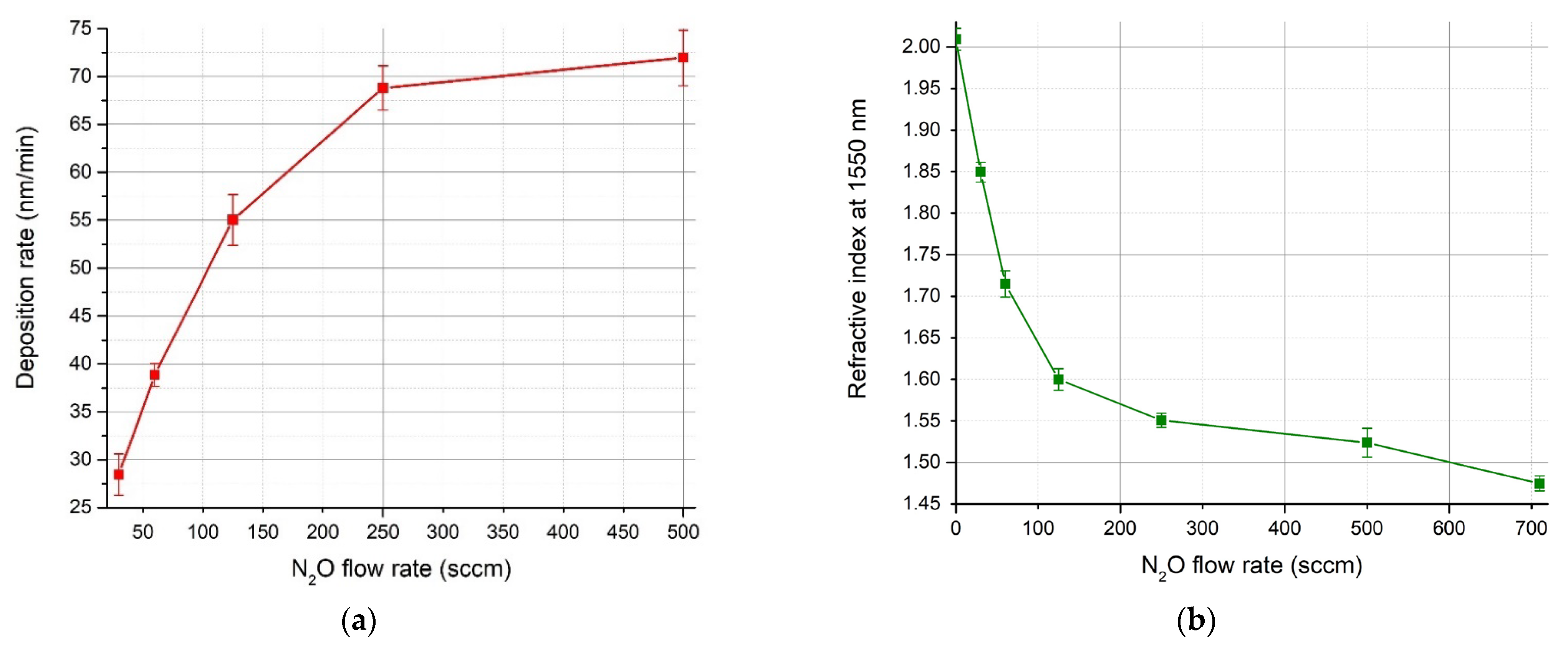
Figure 2a shows the deposition rate (nm/min) of the SiON film as a function of N
2O flow rate resulting from micro-spot spectroscopic reflectometry measurements. The deposition rate of SiON films increases with increasing N
2O flow rate causing more oxygen to be incorporated into the deposited film. It is known that the deposition rate of the SiO
x films fabricated using the PECVD method is several times higher compared to the deposition rate of SiN films. Thus, it is to be expected that the increase of the N
2O flow rate resulted in the higher deposition rate of the SiON film.
Figure 2b shows the refractive index dependence of SiON, SiN, and SiO
x films at λ = 1550 nm on the N
2O flow rate. It is apparent that the refractive index decreases with an increasing N
2O flow rate and has an exponential character. This is explained by the fact that, during the deposition of SiON films utilizing the PECVD method, the most probable reaction is the formation of Si–O bonds. Therefore, even a slight increase of N
2O flow rate, i.e., from 0 to 30 sccm, results in a significant decrease in the refractive index. It is also evident that the refractive index closest to the target value of
n = 1.6 is for the SiON film deposited with N
2O flow rate = 120 sccm.
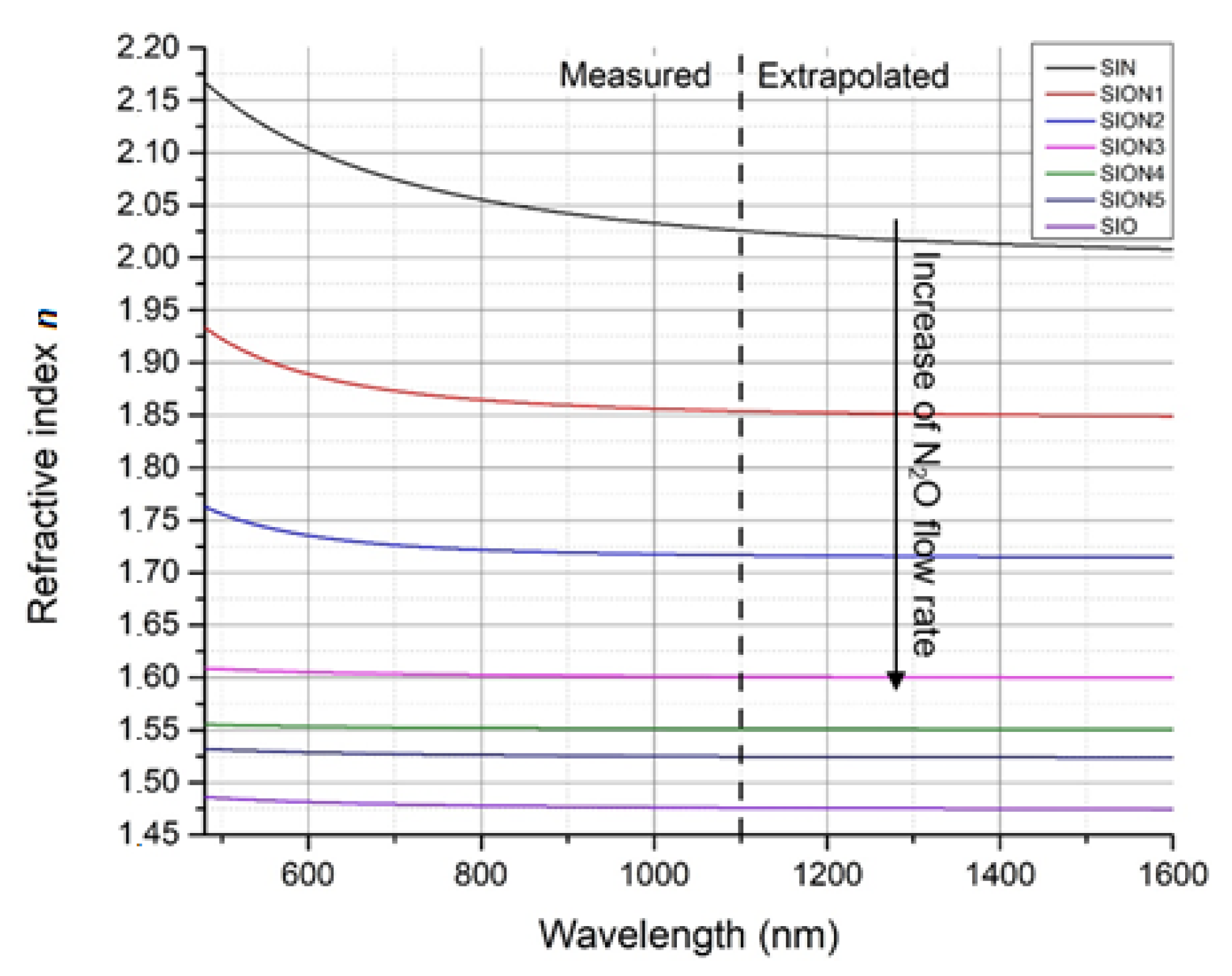
The refractive index as a function of wavelength for SiN, SiO
x, and SiON films is shown in
Figure 3. Functions labeled as SION1–5 in
Figure 3 represent SiON films deposited with N
2O flow rate = 30, 60, 125, 250, and 500 sccm, respectively, as shown in
Table 1. The values in the range from 1100 to 1600 nm were extrapolated from the measured data as the equipment does not allow the measurement in this range. From the analysis of the measured data, it follows that the refractive index of the deposited SiON films can be precisely controlled by the N
2O flow rate. One can also assume that it is possible to increase the refractive index by increasing the NH
3 flow rate. From the results of the analysis, the most suitable gas mixture for the fabrication of films with the target value of the refractive index
n = 1.6 at λ = 1550 nm was the gas mixture of 200(SiH
4):20(NH
3):130(N
2O):600(N
2) sccm.
Figure 4a shows the SIMS analysis of the SiON film with an N
2O flow rate of 30 sccm. In
Figure 4a, the interface between the deposited SiON film and the thermal SiO
2 film and between the thermal SiO
2 film and the Si wafer is visible. The exponential growth of the intensity of all elements in the SiON film is caused by the change of material conductivity with the measurement depth. Unrelated elements with low intensity, i.e., sulfur (S-), nickel (Ni-), carbon (C-, C
2-), and fluorine (F-), are not shown and can be disregarded. From the analysis of all samples, it is clear that the concentration of nitrogen-based elements (SiN-, SiNO- and SiNO
2-) decreases with increasing N
2O flow rate, and the concentration of oxygen based-elements (O-, O
2-, SiO-, and SiO
2-) increases with an increasing N
2O flow rate, as expected. Furthermore, it has been confirmed that the Si–O bonds are dominant over the Si–N bonds in SiON film deposited utilizing the PECVD process. Additionally, the slow increase of deposition rate and a slight decrease of the refractive index at higher N
2O flow rate is caused by saturation of O
2 during the PECVD process. This also confirms the analysis of the refractive index and the deposition rate as functions of the N
2O flow rate shown in
Figure 2a,b.
The standard growth process includes hydrogen as a component from SiH
4 and NH
3. The hydrogen itself is crucial from the absorption peak point of view at λ = 1550 nm. Therefore, it would be useful to estimate the hydrogen concentration level. One method of hydrogen concentration estimation is to compare the relative hydrogen concentration regarding the N
2O flow rate.
Figure 4b shows the relative concentration of hydrogen as a function of N
2O flow rate, where 100% intensity is the intensity measured at an N
2O flow rate of 0 sccm (Si
3N
4 sample). This behavior is not linear and decreases with the N
2O flow rate increase, which is implicit since the overall concentration of gases that contain hydrogen (NH
3, SiH
4) decreases with a increasing N
2O flow rate.
Figure 5a shows the dependence of the refractive index at λ = 1550 nm on the O/(O + N) concentration ratio. The blue squares represent the results acquired from SIMS measurements, and the line represents a calculation of refractive index according to the Bruggeman effective medium approximation method (EMA) [
23,
24] using the following equations:
where
f1 and
f2 are volume fractions of SiO
2 and Si
3N
4 in the SiON film, respectively. Therefore, all oxygen in the SiON film is represented as SiO
2, and all nitrogen is represented as Si
3N
4. The quantity
n1 represents the refractive index of SiO
2,
n2 represents the refractive index of Si
3N
4, and
n is the effective refractive index of SiON film. The value of
n1 was taken as 1.46, and the value of
n2 was 2 in the calculation. Equation (2) is used to convert the volume fraction ratio obtained by Equation (1) into the O/(O + N) concentration ratio. The factor of 1.3 stems from the difference between the atomic concentration of oxygen in SiO
2 (4.64 × 10
22 cm
−3) and that of nitrogen in Si
3N
4 (5.88 × 10
22 cm
−3) [
24]. From
Figure 5a, it is evident that the refractive index decreases with increasing oxygen concentration in the SiON film, as expected. It is also apparent that the refractive index of SiON films calculated with Equations (1) and (2) is quite linear, and the agreement between measurements and calculation is satisfactory. A multiplication of 0.7×O was used as an ionization coefficient for oxygen in the O/(O + N) concentration ratio acquired from SIMS measurements. The other minor differences are caused by ellipsometry and SIMS measurement inaccuracies.
Figure 5b shows the comparison of the O/(O + N) concentration ratio resulting from the SIMS measurement and calculated using Equations (1) and (2) as a function of N
2O gas flow rate. The O/(O + N) concentration ratio increases with the increasing ratio of the N
2O flow rate. This is caused by the oversaturation of O at higher N
2O flow rates. Since the oxygen ionizes easier during SIMS measurements, the O/(O + N) concentration ratio obtained from SIMS measurements is higher at lower N
2O flow rates than the calculated values.
The root mean square (RMS) surface roughness of all films is shown in
Table 1. It is evident that the N
2O flow rate does not affect the RMS surface roughness. The lowest RMS surface roughness is at an N
2O flow rate of 60 sccm, and the highest RMS surface roughness is at an N
2O flow rate of 30 sccm. This RMS surface roughness should not introduce additional optical losses into the SiON waveguides. Even the highest RMS surface roughness measured is much lower than half of the wavelength of transmitted optical signal in the waveguide (1550/1.6 = 969/2 = 484.5 nm). The RMS surface roughness also influences the effective refractive index of SiON films at the interface. However, the RMS roughness below 100 nm is minor compared to the wavelength of propagating light. Therefore, the change of effective refractive index caused by the RMS surface roughness is insignificant and can be neglected.
After the analysis of SiON films with a thickness of ≈500 nm, a 2500 nm thick SiON film with tailored properties was deposited on a 10 µm thick thermal oxide, as mentioned in the section above. The thickness and the uniformity of thickness of the deposited SiON film were analyzed by Micro-spot spectroscopic reflectometry. However, the Cauchy model proved insufficient for the analysis because the difference between the measured and simulated spectral reflectance was too large. Therefore, Scientific Computing International (SCI) model was used for the analysis [
25]. The SCI model is a generalization of the Lorentz oscillator model, where all oscillators are independent. In contrast, the SCI model allows for coupling between the oscillators. As the damping coefficient becomes zero, the SCI model converges to the Lorentz oscillator model. This physical coupling in the generalized model allows accurate simulation of metals, amorphous and crystalline semiconductors, and dielectric materials [
25].
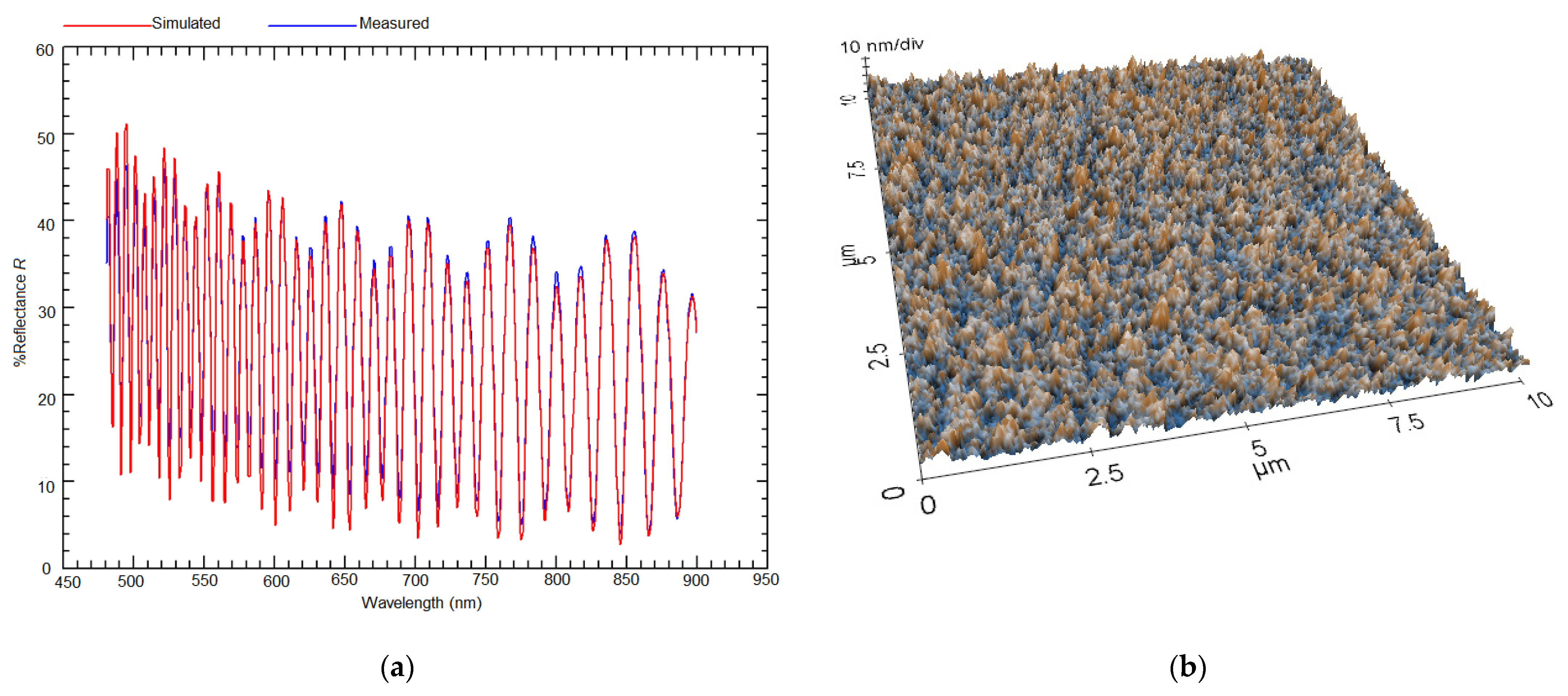
Figure 6a shows the measured and simulated spectral reflectance as a function of wavelength λ. The root mean square error (RMSE) between calculated and measured spectral reflectance is 1.9% which is acceptable. The AFM topography image of the analyzed SiON film is shown in
Figure 6b. The size of the image is 10 × 10 µm
2. In order to emphasize the surface roughness, the
z-axis was magnified 20 times. The RMS surface roughness is approximately 5.32 ± 0.46 nm, which is much lower than the RMS surface roughness measured in the experiment above. One reason for the RMS roughness difference is that different substrates were used for samples with thick films. Another reason could be the technology itself. The RMS roughness below 100 nm is negligible for the waveguide operation, and the influence was not studied further.
Figure 7 shows the thickness and the uniformity of the thickness of SiON films on the whole wafer, where
N is the number of points measured on the wafer. The thickness of SiON film is in the range of 2470–2522 nm, and the uniformity of thickness is ≈1.05%. The average thickness is ≈2505 nm, which is nearly identical to the thickness goal of 2500 nm. From
Figure 7, it is evident that the thickness of the SiON film is the highest in the center of the wafer and decreases from the center to the edges of the wafer.
Figure 8 shows the distribution of refractive index of the SiON film at λ = 1550 nm on the whole wafer, where
N is the number of points measured on the wafer. The distribution is relatively even, with only the edges of the wafer having a refractive index approximately 0.004 higher than the center of the wafer. The refractive index is in the range from
n = 1.588 to
n = 1.598 with an average value of
n = 1.594. The uniformity of the refractive index is 0.3%. This value of the refractive index is relatively close to the desired value of
n = 1.6. The difference is caused by the inaccuracies of the measurement. The extinction coefficient
k is zero.


 ,
, 


