Article

Low-Temperature Epitaxial Growth of AlN Thin Films on a Mo Electrode/Sapphire Substrate Using Reactive Sputtering

Department of Electrical Engineering, Yeungnam University, Gyeongsan 38541, Korea
Coatings 2021, 11(4), 443; https://doi.org/10.3390/coatings11040443
Submission received: 9 March 2021 / Revised: 28 March 2021 / Accepted: 7 April 2021 / Published: 12 April 2021
(This article belongs to the Special Issue Semiconductor Thin Films)

Abstract

:
High-crystalline aluminum nitride (AlN) thin films are essential for device applications, and epitaxial growth is a promising approach to improve their crystalline quality. However, a high substrate temperature is usually required for the epitaxial growth, which is not compatible with the complementary metal-oxide-semiconductor (CMOS) process. Furthermore, it is very difficult to obtain epitaxial AlN thin films on the deposited metal layers that are sometimes necessary for the bottom electrodes. In this work, epitaxial AlN thin films were successfully prepared on a molybdenum (Mo) electrode/sapphire substrate using reactive sputtering at a low substrate temperature. The structural properties, including the out-of-plane and in-plane relationships between the AlN thin film and the substrate, were investigated using X-ray diffraction (XRD) 2θ-ω, rocking curve, and pole figure scans. Additional analyses using scanning electron microscopy (SEM), atomic force microscopy (AFM), and transmission electron microscopy (TEM) were also carried out. It was shown that highly c-axis-oriented AlN thin films were grown epitaxially on the Mo/sapphire substrate with an in-plane relationship of AlN [11 2 ¯ 0]//sapphire [10 1 ¯ 0]. This epitaxial growth was attributed to the highly ordered and oriented Mo electrode layer grown on the sapphire substrate. In contrast, the AlN deposition on the Mo/SiO2/Si substrate under the same conditions caused poorly oriented films with a polycrystalline structure. There coexisted two different low-crystalline phases of Mo (110) and Mo (211) in the Mo layer on the SiO2/Si substrate, which led to the high mosaicity and polycrystalline structure of the AlN thin films.

1. Introduction

Aluminum nitride (AlN) is a versatile III-V compound semiconductor that has emerged as a promising candidate for various applications. Because of its wide bandgap (6.2 eV), AlN is useful for optoelectronic applications, including UV emitters and detectors [1,2,3,4]. It can also be used in high-power/temperature electronics due to its high thermal conductivity, high chemical stability, high-temperature stability, and large dielectric breakdown field [5,6]. In addition, AlN offers interesting properties for microelectromechanical system (MEMS) applications, such as a high acoustic velocity and high piezoelectric coefficients [7,8,9,10].
It is well known that AlN thin films have a hexagonal wurtzite structure with lattice constants of a = 0.311 nm and c = 0.498 nm [11]. The crystalline quality of AlN thin films is very important because it has a great influence on the properties mentioned above. The growth orientation is also significant, especially for MEMS applications. The highly c-axis-oriented growth of AlN thin films is known to be essential for obtaining high piezoelectric coefficients [12]. Therefore, many researchers have devoted considerable effort to developing highly c-axis-oriented AlN thin films with high crystalline quality [13,14,15,16,17,18,19,20]. Epitaxial growth is an attractive method to realize this, and c-plane sapphire is one of the most practical and widely used substrates due to a reasonable lattice mismatch (around 13%) and cost [21,22]. However, high growth temperatures are generally required for epitaxial growth, which in some cases, is not compatible with other fabrication techniques, such as the complementary metal-oxide-semiconductor (CMOS) process. Therefore, the development of a method that allows for the epitaxial growth of AlN thin films at a low temperature is needed.
In some cases, the growth of AlN thin films on deposited metal layers is necessary since there are strong requirements for using bottom electrodes for various applications. For example, most of the electronic devices based on dielectric and piezoelectric properties of AlN need underlying conducting layers [14]. In order to acquire highly crystalline and c-axis-oriented AlN thin films on a metal electrode, the appropriate selection of the bottom electrode material is necessary since the structural and surface properties of the deposited metal are extremely different from those of a single-crystalline substrate. Among many materials, molybdenum (Mo) is a strong candidate owing to its high electrical conductivity, small difference in thermal expansion coefficient, and good adhesion to AlN [23,24,25]. However, although Mo has such advantages, it is not easy to obtain highly c-axis-oriented AlN thin films on a Mo electrode. Moreover, it is even more difficult to grow epitaxial AlN thin films because the deposited metal layers have relatively low crystalline quality. As far as we are aware, there are no previous reports on the epitaxial growth of AlN thin films on a Mo electrode. If the epitaxial growth is feasible, it would be ideal for applications that require a bottom electrode and highly crystalline AlN thin films.
In this study, the epitaxial growth of AlN thin films on a Mo electrode/sapphire substrate at a low substrate temperature using reactive sputtering was explicitly demonstrated. A Mo thin film with a sufficient thickness of 100 nm was deposited as the bottom electrode on a sapphire substrate. After that, a highly c-axis-oriented AlN thin film was successfully grown epitaxially on the Mo electrode. The compatibility with the CMOS process was also maintained by limiting the substrate temperature to 350 °C without any additional annealing step. For comparison, an AlN thin film on a Mo electrode/SiO2/Si substrate was also prepared under the same deposition conditions. To investigate the structural properties of the AlN thin films, X-ray diffraction (XRD) 2θ-ω, rocking curve, and pole figure scans were carried out. Additional analyses using scanning electron microscopy (SEM), atomic force microscopy (AFM), and transmission electron microscopy (TEM) were also undertaken.

2. Experimental

Every sample was prepared using a customized pulsed DC magnetron sputtering system. Two metal targets (Mo and Al) with a diameter of 100 mm were mounted on the upper side of the process chamber, and a 4-inch substrate was placed 100 mm away from the target on a substrate chuck. The substrate was heated using a SiC heater and rotated during the deposition for better uniformity. Before preparing the samples, the target angle was adjusted to provide the optimal incident angle of the sputtered particles. The angle was determined experimentally in advance by measuring the uniformity of the deposited films. The sputtering chamber was pumped down to below 6.6 × 10⁻⁵ Pa prior to every deposition. A Mo thin film was deposited in situ on a sapphire (001) substrate at a substrate temperature of 300 °C using a pulsed DC power of 300 W and the Mo metal target in an Ar atmosphere. The pulse frequency was kept at 20 kHz with a duty cycle of 45%. After that, the Al target was sputtered in a reactive nitrogen atmosphere with an Ar–N2 gas mixture for the deposition of a 200 nm thick AlN thin film. The deposition was carried out at a working pressure of 0.32 Pa and a DC power of 500 W. The substrate temperature was maintained at 350 °C. The same process was applied to a SiO2/Si substrate to prepare an AlN thin film on the Mo electrode/SiO2/Si substrate for comparison. The structural properties of the AlN thin films were analyzed using a high-resolution XRD (PANalytical, Almelo, The Netherlands) with CuKα radiation. XRD 2θ-ω, rocking curve, and pole figure scans were carried out to identify the in-plane and out-of-plane orientations of the films. The surface morphology and cross-section of the AlN thin films were observed using SEM (TESCAN, Brno, Czech Republic) and AFM (JPK instruments, Berlin, Germany). TEM (JEOL, Tokyo, Japan) combined with a focused ion beam (FIB) tool was also utilized to evaluate the crystalline properties in more detail.

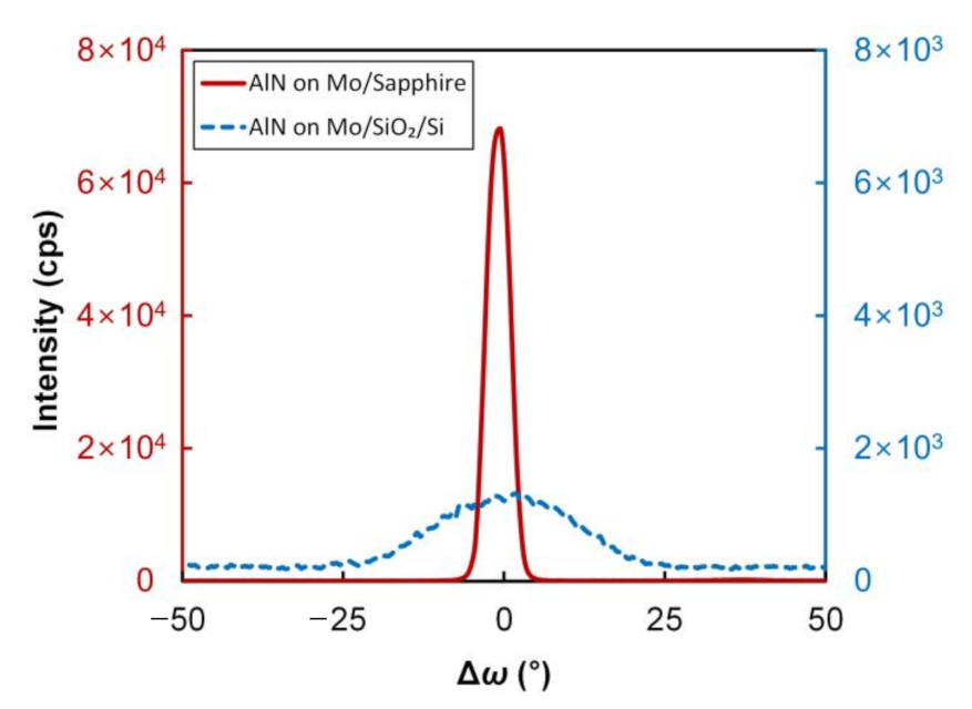
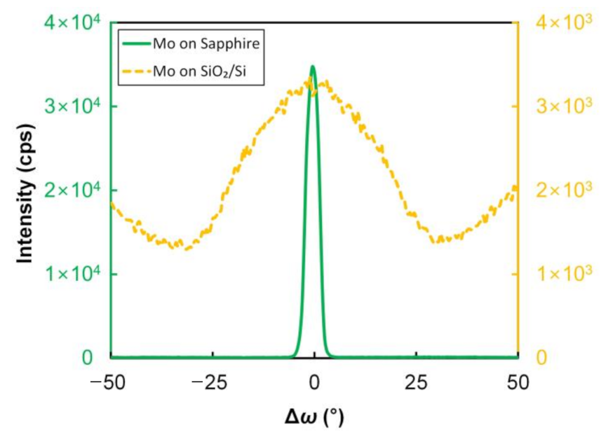
3. Results and Discussion

Figure 1 shows the results of XRD 2θ-ω scan for the AlN thin film on the Mo electrode/sapphire substrate (red) and the Mo electrode/SiO2/Si substrate (blue). It can be clearly seen that the diffraction peaks of AlN (002) and AlN (004) appeared at around 2θ = 36.1° and 76.5° for the AlN thin film on the Mo/sapphire substrate (The International Centre for Diffraction Data (ICDD) No. 00-025-1133). The diffraction peaks at around 2θ = 40.9° and 2θ = 41.8° corresponded to Mo (110) and sapphire (006), respectively (ICDD No. 00-042-1120 and 00-046-1212). These results imply that a c-axis-oriented AlN thin film was grown on the Mo electrode. In addition, it can be stated that the Mo electrode layer was also formed with a preferred orientation along the (110) crystallographic plane. However, quite different results were observed for the AlN thin film on the Mo/SiO2/Si substrate. The peak of AlN (002) was also appeared, but the intensity of the peak was much weaker, indicating a poor crystallization degree of the AlN thin film on the Mo/SiO2/Si substrate. In addition, the peak of Mo (110) was considerably weaker, and there was an additional peak at around 2θ = 74.1° corresponding to Mo (211). This means that the Mo electrode layer had also a low crystallinity and was not highly oriented. The peaks at 2θ = 33.0° and 2θ = 69.2° were caused by the diffraction from the Si substrate (ICDD No. 00-027-1402).
The crystalline quality, namely, the distribution of preferred orientation, was further analyzed using XRD rocking curve measurements. Figure 2 shows the comparison of the XRD rocking curves of AlN (002) on the Mo/sapphire and Mo/SiO2/Si substrates. The diffraction peak from the AlN thin film on the Mo/sapphire substrate was much stronger and sharper than that from the AlN thin film on the Mo/ SiO2/Si substrate. The full width at half maximum (FWHM) value calculated from the former was 4.15° while the FWHM from the latter was larger than 13°, which indicates that the degree of orientation of the AlN thin film on the Mo/sapphire substrate was much higher than that on the Mo/SiO2/Si substrate. In addition, whereas only a single peak was detected for the AlN thin film on the Mo/sapphire substrate, extra signals (not 0) appeared on either side of the central peak for the AlN thin film on the Mo/SiO2/Si substrate, which indicates a poorly oriented AlN thin film on the Mo/SiO2/Si substrate with high mosaicity.
It should be pointed out that the structural properties of the Mo electrode on the sapphire and SiO2/Si substrates were revealed to be different from each other in the XRD 2θ-ω scan (Figure 1). While the Mo electrode layer on the sapphire substrate was grown with a preferred orientation in the (110) plane, the Mo layer on the SiO2/Si substrate was not highly oriented and had low crystallinity. This seemed to affect the growth of the AlN thin films in the succeeding deposition. Thus, to evaluate the degree of orientation of the Mo, the XRD rocking curve was taken again by measuring the (110) reflection of the Mo layers without the AlN depositions. Figure 3 shows the comparison of the XRD rocking curves of Mo (110) on the sapphire and SiO2/Si substrates. As expected, the Mo electrode layer on the sapphire substrate showed a considerably stronger and sharper peak, implying a high degree of orientation. However, on the SiO2/Si substrate, the low crystalline quality of the Mo layer was verified. The existence of other phases besides Mo (110) was also confirmed by detecting the additional broad components on either side of the peak, which is in good agreement with the 2θ-ω scan result shown in Figure 1.
The in-plane orientational relationship between the AlN thin film and sapphire substrate was verified using XRD pole figure measurements. Figure 4a shows the XRD pole figure of AlN (101) from the AlN thin film on the Mo/sapphire substrate. The AlN (101) poles appeared at six symmetrical positions separated by 60° (φ) at around ψ = 61.5°, which strongly suggests that the AlN thin film was grown epitaxially along the c-axis on the Mo/sapphire substrate. The negligibly weak central pattern was presumably due to the effect of the Mo (110). The pole figure of AlN (002) from the AlN thin film on the Mo/sapphire substrate is depicted in Figure 4b to illustrate the in-plane relationship. The clear evidence of the c-axis-oriented growth of the AlN thin film was confirmed again by detecting the very strong central pole. The three sharp symmetrical poles separated by 120° (φ) indicated the sapphire (104), which has a similar d-spacing to AlN (002). By comparing these three symmetrical poles with the six symmetrical AlN (101) poles in Figure 4a, the in-plane relationship between the AlN thin film and the sapphire substrate was defined. The three symmetrical sapphire (104) poles appeared with a 30° shift in the azimuthal angle relative to the six symmetrical AlN (101) poles; therefore, it can be said that the AlN thin film was grown epitaxially with a 30° rotation of the unit cell with respect to the sapphire substrate. That is to say, the in-plane orientational relationship between the AlN thin film and sapphire substrate was defined as AlN [11 2 ¯ 0]//sapphire [10 1 ¯ 0]. These results agree with other studies suggesting that epitaxial growth of AlN thin films can be achieved on sapphire substrates with an in-plane rotation of 30° [26,27,28,29]. This rotation is caused by the lattice mismatch between the AlN and the sapphire substrate. Because sapphire has a lattice constant of a = 0.476 nm, there exists a lattice mismatch of around 34.6% relative to AlN thin films. However, with this rotation, the lattice mismatch can decrease to 13.4%, which enables the epitaxial growth of AlN thin films [26]. In this work, it should be emphasized that there was a Mo electrode between the AlN thin film and the sapphire substrate. It was confirmed that the epitaxial growth of the AlN thin films could still be achieved even on the Mo electrode formed on the sapphire substrate, and the Mo layer could transfer the crystallographic information of the underlying sapphire substrate to the AlN thin films. For comparison, the XRD pole figure of AlN (101) from the AlN thin film on the Mo/SiO2/Si substrate is depicted in Figure 4c. The relatively strong ring pattern at around ψ = 61.5° indicates that the AlN thin film was grown with no preferred in-plane orientation, which means that a polycrystalline structure was present. Furthermore, it was easily shown by other weak irregular patterns that the AlN thin film on the Mo/SiO2/Si substrate was not highly c-axis-oriented.
The surface morphology of the AlN thin film on the Mo/sapphire substrate that was observed using SEM is shown in Figure 5a. High-density crystal grains with a diameter of less than 20 nm can be seen, indicating the three-dimensional growth mode of the sputtering [30]. In contrast, in the case of the AlN thin film on the Mo/SiO2/Si substrate, separations of the grains with clear and wide grain boundaries are shown in the SEM image in Figure 5c. As described above, the AlN thin film on the Mo/SiO2/Si substrate tended to grow without a preferred orientation parallel to the surface, and this is directly revealed in Figure 5c. The growth disorder in the AlN thin film caused the wide grain boundaries on the surface. The cross-sectional SEM images of the AlN thin film on the Mo/sapphire and Mo/SiO2/Si substrates are presented in Figure 5b,d. Figure 5b clearly reveals the growth of the AlN thin film with a columnar structure on the Mo/sapphire substrate. However, a relatively irregular structure due to the low crystalline quality was observed for the AlN thin film on the Mo/SiO2/Si substrate in Figure 5d.
The AFM images of the AlN thin film on the Mo/sapphire and Mo/SiO2/Si substrates are depicted in Figure 6a,b. The AFM analysis revealed a low root-mean-square (RMS) surface roughness of 1.06 nm for the AlN thin film on the Mo/sapphire substrate. However, the AlN thin film on the Mo/SiO2/Si substrate showed a higher RMS surface roughness of 2.06 nm. It was confirmed that the surface morphology and roughness of both samples observed using AFM corresponded with the SEM results in Figure 5a,c.
Figure 7a shows the cross-sectional bright-field TEM image of the AlN thin film on the Mo/sapphire substrate structure. The high-resolution image of the AlN thin film is also presented in Figure 7b. The Mo electrode layer exhibited a preferentially oriented columnar structure. In addition, as already observed in Figure 5b, the AlN thin film also had a successive columnar structure that was highly ordered and c-axis-oriented. These results are consistent with the findings from the XRD analysis described above showing that the Mo electrode on the sapphire substrate was well oriented and the high-crystalline AlN thin film was grown epitaxially on it. It should be noticed in the XRD results that the Mo electrode on the SiO2/Si substrate was not highly oriented, that is, there coexisted at least two different low-crystalline phases of Mo (110) and Mo (211). As a result, the AlN thin film on the Mo/SiO2/Si substrate was also poorly oriented and had a polycrystalline structure. Therefore, the epitaxial growth is considered to be attributed to the highly ordered and oriented Mo electrode layer grown on the sapphire substrate. The epitaxial growth of the AlN thin film on the Mo/sapphire substrate was confirmed again in the selected area electron diffraction (SAED) pattern that is shown in Figure 7c. From these results, it can be concluded that highly c-axis-oriented AlN thin films can be grown epitaxially on the Mo/sapphire substrate, where this growth behavior will be very useful for practical applications requiring high-quality AlN thin films and bottom electrodes.

4. Conclusions

It was shown that AlN thin films could be grown epitaxially on a Mo electrode/sapphire substrate using reactive sputtering at a low substrate temperature. Highly c-axis-oriented epitaxial AlN thin films were obtained with an in-plane relationship of AlN [11 2 ¯ 0]//sapphire [10 1 ¯ 0]. The well-oriented Mo electrode layer on the sapphire substrate led to the epitaxial growth of AlN thin films with high crystalline quality. On the other hand, in the case of the AlN thin film on the Mo electrode/SiO2/Si substrate, because of the coexistence of the different low-crystalline phases, that is, Mo (110) and Mo (211) in the Mo layer, the AlN thin film had a polycrystalline structure with high mosaicity. This work demonstrated the possibility of the epitaxial growth of AlN thin films, even on an underlying metal electrode, which will be beneficial for several application areas. Further study on the effects of the epitaxial growth on various material properties and device applications using the Mo bottom electrode will be the subject of future work.

Funding

This research was supported by a Yeungnam University Research Grant (220A580080).

Institutional Review Board Statement

Not applicable.

Informed Consent Statement

Not applicable.

Data Availability Statement

Data is contained within the article.

Acknowledgments

The author thanks Korea Basic Science Institute (KBSI) in Daegu, Korea, for XRD measurements.

Conflicts of Interest

The author declares no conflict of interest.

References

  1. Bairagi, S.; Järrendahl, K.; Eriksson, F.; Hultman, L.; Birch, J.; Hsiao, C. Glancing Angle Deposition and Growth Mechanism of Inclined AlN Nanostructures using Reactive Magnetron Sputtering. Coatings 2020, 10, 768. [Google Scholar] [CrossRef]
  2. Bayerl, D.; Islam, S.M.; Jones, C.M.; Protasenko, V.; Jena, D.; Kioupakis, E. Deep Ultraviolet Emission from Ultra-Thin GaN/AlN Heterostructures. Appl. Phys. Lett. 2016, 109, 241102. [Google Scholar] [CrossRef]
  3. Chen, G.; Zhang, Y.; Zhang, H.; Xie, L.; Xing, Z.; Cheng, Z.; Li, H.; Xiao, Y.; Liang, H.; Liu, H. Ultraviolet Optical Properties Analysis of Wurtzite AlN Films Grown by Vapor Phase Epitaxy. Opt. Mater. 2021, 111, 110678. [Google Scholar] [CrossRef]
  4. Li, T.; Wang, F.; Lin, R.; Xie, W.; Li, Y.; Zheng, W.; Huang, F. In-Plane Enhanced Epitaxy for Step-Flow AlN Yielding a High-Performance Vacuum-Ultraviolet Photovoltaic Detector. CrystEngComm 2020, 22, 654–659. [Google Scholar] [CrossRef]
  5. Motamedi, P.; Cadien, K. XPS Analysis of AlN Thin Films Deposited by Plasma Enhanced Atomic Layer Deposition. Appl. Surf. Sci. 2014, 315, 104–109. [Google Scholar] [CrossRef]
  6. Kim, T.; Kim, J.; Dalmau, R.; Schlesser, R.; Preble, E.; Jiang, X. High-Temperature Electromechanical Characterization of AlN Single Crystals. IEEE Trans. Ultrason. Ferroelectr. Freq. Control 2015, 62, 1880–1887. [Google Scholar] [CrossRef] [PubMed]
  7. Tonisch, K.; Cimalla, V.; Foerster, C.; Romanus, H.; Ambacher, O.; Dontsov, D. Piezoelectric Properties of Polycrystalline AlN Thin Films for MEMS Application. Sens. Actuators A Phys. 2006, 132, 658–663. [Google Scholar] [CrossRef]
  8. Ababneh, A.; Alsumady, M.; Seidel, H.; Manzaneque, T.; Hernando-García, J.; Sánchez-Rojas, J.L.; Bittner, A.; Schmid, U. C-Axis Orientation and Piezoelectric Coefficients of AlN Thin Films Sputter-Deposited on Titanium Bottom Electrodes. Appl. Surf. Sci. 2012, 259, 59–65. [Google Scholar] [CrossRef]
  9. Musa, I.; Qamhieh, N.; Said, K.; Mahmoud, S.T.; Alawadhi, H. Fabrication and Characterization of Aluminum Nitride Nanoparticles by RF Magnetron Sputtering and Inert Gas Condensation Technique. Coatings 2020, 10, 411. [Google Scholar] [CrossRef] [Green Version]
  10. Jackson, N.; Keeney, L.; Mathewson, A. Flexible-CMOS and Biocompatible Piezoelectric AlN Material for MEMS Applications. Smart Mater. Struct. 2013, 22, 115033. [Google Scholar] [CrossRef]
  11. Galca, A.C.; Stan, G.E.; Trinca, L.M.; Negrila, C.C.; Nistor, L.C. Structural and Optical Properties of C-Axis Oriented Aluminum Nitride Thin Films Prepared at Low Temperature by Reactive Radio-Frequency Magnetron Sputtering. Thin Solid Films 2012, 524, 328–333. [Google Scholar] [CrossRef]
  12. Iriarte, G.F.; Rodríguez, J.G.; Calle, F. Synthesis of C-Axis Oriented AlN Thin Films on Different Substrates: A Review. Mater. Res. Bull. 2010, 45, 1039–1045. [Google Scholar] [CrossRef]
  13. Imran, S.; Yuan, J.; Yin, G.; Ma, Y.; He, S. Influence of Metal Electrodes on C-axis Orientation of AlN Thin Films Deposited by DC Magnetron Sputtering. Surf. Interface Anal. 2017, 49, 885–891. [Google Scholar] [CrossRef]
  14. Pawar, S.; Singh, K.; Sharma, S.; Pandey, A.; Dutta, S.; Kaur, D. Growth Assessment and Scrutinize Dielectric Reliability of C-Axis Oriented Insulating AlN Thin Films in MIM Structures for Microelectronics Applications. Mater. Chem. Phys. 2018, 219, 74–81. [Google Scholar] [CrossRef]
  15. Alizadeh, M.; Mehdipour, H.; Ganesh, V.; Ameera, A.N.; Goh, B.T.; Shuhaimi, A.; Rahman, S.A. Plasma-Assisted Hot Filament Chemical Vapor Deposition of AlN Thin Films on ZnO Buffer Layer: Toward Highly C-Axis-Oriented, Uniform, Insulative Films. Appl. Phys. A 2014, 117, 2217–2224. [Google Scholar] [CrossRef]
  16. Tavsanoglu, T. Synthesis of C-Axis Oriented AlN Thin Films at Room Temperature. Surf. Eng. 2017, 33, 249–254. [Google Scholar] [CrossRef]
  17. Jiang, J.; Peng, B.; Zhang, W.; Wang, Y.; Shu, L.; Wang, R. Growth of C-Axis Oriented AlN Thin Films on Titanium Alloy Substrate by Middle Frequency Magnetron Sputtering. J. Vac. Sci. Technol. A Vac. Surf. Film. 2015, 33, 041509. [Google Scholar] [CrossRef]
  18. Monteagudo-Lerma, L.; Naranjo, F.B.; González-Herráez, M.; Fernández, S. Influence of Substrate Biasing on the Growth of C-axis Oriented AlN Thin Films by RF Reactive Sputtering in Pure Nitrogen. Phys. Status Solidi C 2012, 9, 1074–1078. [Google Scholar] [CrossRef]
  19. Wistrela, E.; Schneider, M.; Bittner, A.; Schmid, U. Impact of the Substrate Dependent Polarity Distribution in C-Axis Oriented AlN Thin Films on the Etching Behaviour and the Piezoelectric Properties. Microsyst. Technol. 2016, 22, 1691–1700. [Google Scholar] [CrossRef]
  20. Pandey, A.; Kaushik, J.; Dutta, S.; Kapoor, A.K.; Kaur, D. Electrical and Structural Characteristics of Sputtered C-Oriented AlN Thin Films on Si (100) and Si (110) Substrates. Thin Solid Films 2018, 666, 143–149. [Google Scholar] [CrossRef]
  21. Zhang, X.; Xu, F.J.; Wang, J.M.; He, C.G.; Zhang, L.S.; Huang, J.; Cheng, J.P.; Qin, Z.X.; Yang, X.L.; Tang, N. Epitaxial Growth of AlN Films on Sapphire via a Multilayer Structure Adopting a Low-and High-Temperature Alternation Technique. CrystEngComm 2015, 17, 7496–7499. [Google Scholar] [CrossRef]
  22. Paduano, Q.S.; Weyburne, D.W.; Jasinski, J.; Liliental-Weber, Z. Effect of Initial Process Conditions on the Structural Properties of AlN Films. J. Cryst. Growth 2004, 261, 259–265. [Google Scholar] [CrossRef]
  23. Yang, J.; Jiao, X.; Zhang, R.; Zhong, H.; Shi, Y.; Du, B. Growth of AlN Films as a Function of Temperature on Mo Films Deposited by Different Techniques. J. Electron. Mater. 2014, 43, 369–374. [Google Scholar] [CrossRef]
  24. Kamohara, T.; Akiyama, M.; Ueno, N.; Kuwano, N. Improvement in Crystal Orientation of AlN Thin Films Prepared on Mo Electrodes using AlN Interlayers. Ceram. Int. 2008, 34, 985–989. [Google Scholar] [CrossRef]
  25. Chauhan, S.S.; Joglekar, M.M.; Manhas, S.K. Influence of Process Parameters and Formation of Highly C-Axis Oriented AlN Thin Films on Mo by Reactive Sputtering. J. Electron. Mater. 2018, 47, 7520–7530. [Google Scholar] [CrossRef]
  26. Seo, H.; Petrov, I.; Kim, K. Structural Properties of AlN Grown on Sapphire at Plasma Self-Heating Conditions using Reactive Magnetron Sputter Deposition. J. Electron. Mater. 2010, 39, 1146–1151. [Google Scholar] [CrossRef]
  27. Six, S.; Gerlach, J.W.; Rauschenbach, B. Epitaxial Aluminum Nitride Films on Sapphire Formed by Pulsed Laser Deposition. Thin Solid Films 2000, 370, 1–4. [Google Scholar] [CrossRef]
  28. Okamoto, M.; Mori, Y.; Sasaki, T. Epitaxial Growth of AlN Thin Films on Sapphire by Pulsed Laser Deposition and Effect of N2 Ambient on Crystallinity. Jpn. J. Appl. Phys. 1999, 38, 2114. [Google Scholar] [CrossRef]
  29. He, C.; Zhao, W.; Wu, H.; Zhang, S.; Zhang, K.; He, L.; Liu, N.; Chen, Z.; Shen, B. High-Quality AlN Film Grown on Sputtered AlN/Sapphire Via Growth-Mode Modification. Cryst. Growth Des. 2018, 18, 6816–6823. [Google Scholar] [CrossRef]
  30. Zhao, L.; Yang, K.; Ai, Y.; Zhang, L.; Niu, X.; Lv, H.; Zhang, Y. Crystal Quality Improvement of Sputtered AlN Film on Sapphire Substrate by High-Temperature Annealing. J. Mater. Sci. Mater. Electron. 2018, 29, 13766–13773. [Google Scholar] [CrossRef]
Figure 1. X-ray diffraction (XRD) 2θ-ω scan patterns for the AlN thin films on the Mo electrode/sapphire and Mo electrode/SiO2/Si substrates.
Coatings 11 00443 g001
Figure 2. Comparison of the XRD rocking curves of AlN (002) on the Mo/sapphire and Mo/SiO2/Si substrates.
Coatings 11 00443 g002
Figure 3. Comparison of the XRD rocking curves of Mo (110) on the sapphire and SiO2/Si substrates.
Coatings 11 00443 g003
Figure 4. XRD pole figure pattern of (a) AlN (101) from the AlN thin film on the Mo/sapphire substrate, (b) AlN (002) from the AlN thin film on the Mo/sapphire substrate, and (c) AlN (101) from the AlN thin film on the Mo/SiO2/Si substrate.
Coatings 11 00443 g004
Figure 5. Scanning electron microscopy (SEM) images of the AlN thin film. (a) Top-view and (b) cross-sectional view of the AlN thin film on the Mo/sapphire substrate. (c) Top-view and (d) cross-sectional view of the AlN thin film on the Mo/SiO2/Si substrate.
Coatings 11 00443 g005
Figure 6. Atomic force microscopy (AFM) images of the AlN thin film on (a) the Mo electrode/sapphire substrate and (b) the Mo electrode/SiO2/Si substrate.
Coatings 11 00443 g006
Figure 7. (a) Cross-sectional transmission electron microscopy (TEM) image of the AlN thin film on the Mo/sapphire substrate structure. (b) High-resolution TEM image and (c) selected area electron diffraction (SAED) pattern of the AlN thin film on the Mo/sapphire substrate.
Coatings 11 00443 g007
Publisher’s Note: MDPI stays neutral with regard to jurisdictional claims in published maps and institutional affiliations.

