Article

Influence of the Physical Properties on the Antibacterial and Photocatalytic Behavior of Ag-Doped Indium Sulfide Film Deposited by Spray Pyrolysis

1
Laboratory of Physics of Materials and Nanomaterials Applied at Environment, Faculty of Sciences in Gabes, Gabes University, Cité Erriadh, Zrig, 6072 Gabes, Tunisia
2
Unité de Recherche Matériaux Avancés et Nanotechnologies (URMAN), Institut Supérieur des Sciences, Appliquées et de Technologie de Kasserine, Kairouan University, BP 471 Kasserine 1200, Tunisia
3
Materials Science and Engineering Faculty, Transilvania University, 500036 Brasov, Romania
4
Department of Materials and Products Characterization for Electrical and Energy Engineering, R&D National Institute for Electrical Engineering ICPE-CA Bucharest, 030138 Bucharest, Romania
5
Physics Center of Minho and Porto Universities—CF-UM-UP, University of Minho, Campus de Gualtar, 4710-057 Braga, Portugal
*
Authors to whom correspondence should be addressed.
Coatings 2021, 11(4), 370; https://doi.org/10.3390/coatings11040370
Submission received: 19 February 2021 / Revised: 15 March 2021 / Accepted: 19 March 2021 / Published: 24 March 2021
(This article belongs to the Collection Feature Paper Collection in Thin Films)

Abstract

:
Spray pyrolysis was used to deposit indium sulfide (In2S3) films, with or without silver doping. The films are polycrystalline, and the inclusion of Ag in the In2S3 structure leads to the formation of a solid solution, with the crystallite size of the order of tens of nanometers. In2S3 films exhibit a semiconductive behavior, and the incorporation of Ag leads to an increase of the charge carrier concentration, enhancing the electrical conductivity of the films. The small polaron hopping mechanism, deduced by the fittings according to the double Jonscher variation, explains the evolution of the direct current (dc) conductivity at high temperature of the Ag-doped indium sulfide. From impedance spectroscopy, it was found that the doped film presents dielectric relaxation, and Nyquist diagrams indicate the importance of the grain and the grain boundaries’ contributions to the transport phenomena. The physical characteristics of the films have an influence on the photocatalytic performance, achieving photodegradation efficiency above 80% (85.5% in the case of Ag doping), and on the antibacterial activity. The obtained results indicate that indium sulfide films are good candidates for environmental and biological applications, confirming a multifunctional nature.

1. Introduction

Environmental pollution, energy efficiency, pharmaceutical research, and biomaterials are some of the hot topics of today’s world. Toxic organic pollutants are harmful to human beings and hinder sustainable development [1,2]. Some of these fields work in opposite directions. As an example, pharmaceutical research is extremely important, but the resultant pollution by antimicrobial agents, for instance, can be a huge problem. One of the most promising solutions for the degradation of various types of antibiotic contaminants is performed by semiconductor-based heterogeneous photocatalysis. This approach has received considerable attention, particularly because it is an environmentally friendly technology [3,4,5]. Under sunlight, photocatalysis may break the chemical bonds in water and produce oxygen and hydrogen, helping the removal of contaminants. Using photocatalysis to degrade contaminants may help solve some of the environmental problems [6,7,8]. To degrade organic pollutants, various semiconductors such as metal oxides (ZnO/In2O3, TiO2), sulfides (CdS), halides (APbBr4), organometallic complexes (MMCs), and other metal-free (FeP/g-C3N4) photocatalysts have been widely studied and used in many photocatalytic applications [9,10,11,12,13]. Among popular semiconductors, indium sulfide (In2S3) is a promising material that has generated enthusiasm in the domain of photocatalysis investigation. In2S3 is classified as an n-type III–VI chalcogenide semiconductor [14]. It reveals direct band gap energy, ranging from 2.0 to 3.0 eV and high transmittance in the visible and near-infrared regions of the electromagnetic spectrum [15,16]. At atmospheric pressure, In2S3 may appear in three allotropic forms (α, β, and γ) with phase transitions at temperatures of 420 and 754 °C, respectively [17]. Thermodynamically, the most stable form is β-In2S3, which was reported to exhibit exceptional optoelectronic performances [18]. This β form has been widely considered for photocatalysis, photovoltaic systems, antibacterial activity [19,20,21,22], and also as a photosensor material. It has been reported that solar cell devices using β-In2S3 as a buffer layer provide a fractional conversion value close to that of the standard cadmium sulfide (CdS) buffer layer (16.4%) [23]. Due to the high toxicity of Cd2+, and having in mind the pollution reduction, researchers reported that Cd2+ can be replaced by In3+ ions because of its low toxicity [24]. Different types of micro/nanostructures of β-In2S3 can be prepared by different synthesis methods [18,25,26,27,28,29,30,31,32]. Among the reported techniques, spray pyrolysis is a good choice to obtain In2S3 nanostructured layers and has the capacity to prepare thin films on large surfaces, easily and with low cost. This is particularly important for industrial production. Spray pyrolysis is also important to produce films for photocatalysis because it is possible to produce films with a high specific surface area (surface area/volume ratio) due to the relatively high roughness of the surface of the produced films [33]. In2S3 thin films deposited by the spray pyrolysis technique have relatively high electrical resistivity. Although some properties of this material are adequate for certain applications, sometimes higher conductivity might be needed [34]. The stable phases of intrinsic In2S3 may show limited electrical conductivity for certain applications due to its forbidden band energy. Doping the host materials with metal elements (Cu, Al, Mn, Ag, etc.) alters the electronic and optical properties relative to the intrinsic material and is one of the effective techniques to improve these properties of a material [35,36,37,38]. For example, Poudel et al. describe the incorporation of Ag nanoparticles to enhance the electrochemical performance of materials for electrodes of molybdenum sulfide and tungsten [39]. Other authors observed that Ag incorporation affects the physical properties of In2S3, particularly the electrical properties, leading to decrease of the electrical resistivity due to an increase of the concentration of electric charge carriers [40,41,42,43].
Despite the bibliography about In2S3, only few studies have been interested in electrical properties but not in detail. In this work, a very detailed work on the electrical behavior has been done, namely direct current (dc) and alternating current (ac) conductivity, conduction mechanism, activation energy, relaxation time, grains and grains boundaries’ conductivity contribution, and Ag doping. Moreover, the correlation between the physical properties (structure, morphology, electrical) and photodegradation efficiency as well as the antibacterial activity was also investigated.

2. Materials and Methods

Indium sulfide films were deposited by spray pyrolysis on microscope glass substrates (1 cm × 1 cm) at 350 °C. The films were prepared by spraying 50 mL of aqueous solution containing 0.1106 g of indium chloride (InCl3) and 0.1142 g of thiourea (SC(NH2)2), as precursors. To produce the Ag-doped indium sulfide sample, 0.0014 g of silver nitrate (AgNO3) was added to the solution. The solutions were sprayed at a flow rate of 2.6 mL/min onto the glass substrates. The composition of the films was obtained by energy-dispersive X-ray spectroscopy (EDX) using a Zeiss FESEM Ultra Plus scanning electron microscope (Zeiss, Oberkochen, Germany). The atomic compositions are presented in Table 1. From this point forward, the undoped and Ag-doped films will be referred as In2S3 and In2S3:Ag, respectively. Detailed explanations about the experimental protocols for the fabrication of the indium sulfide thin films can be found in a previous work [44].
Structural analysis by X-ray diffraction (XRD) was performed using BRUKER-ADVANCE D8 diffractometer (Bruker, Billerica, MA, USA). A CuKα source with a wavelength of 1.5418 Å was used. The XRD patterns were obtained in the range of 20° < 2θ < 70°, with step size of 0.02°.
Morphological examination and the determination of surface roughness were performed by atomic force microscopy (AFM, NT-MDT Spectrum Instruments, Moscow, Russia) at room temperature, using a Pro-M NT-MDT system, in non-contact mode (NC-AFM). AFM scans on random zones were carried out. The 2D and 3D AFM images were processed using Nova software.
The electrical characterization was carried out by electrical impedance spectroscopy (EIS), using an Agilent 4294A impedance analyzer (Keysight, Santa Rosa, CA, USA). Prior to the measurements, two silver electrodes (28 nm thick) were deposited on the surface of the films. The range of frequencies and temperatures explored were between 40 Hz and 110 MHz, and 460 to 600 K, respectively. The alternating excitation signal had an amplitude of 50 mV.
The photocatalysis experiments consisted in the degradation of a methylene blue (MB) solution (initial concentration of 10−5 M and pH = 6.5) under visible-light irradiation. The films, deposited on the microscope glass substrates, were submerged in 10 mL of MB solution, inside a closed cylindrical reactor containing four light bulbs, irradiating in the visible region of the electromagnetic spectrum, for 270 min, at room temperature (22 °C).
Absorbance spectra of the MB solution, before and after irradiation, were obtained with a Dynamica Halo XB-10 spectrophotometer (Dynamica Scientific Ltd., Livingston, UK). The estimation of the MB concentration after the 270 min irradiation ( c f i n a l ), was estimated by the absorbance value of the solution, at λ = 665 nm, and using a calibration curve. The photodegradation efficiency (η) was obtained by using Equation (1):
η % = c i n i t i a l c f i n a l c i n i t i a l × 100
The antibacterial tests were performed on In2S3:Ag films, sterilized in an autoclave (Prestige Medical Classic, Blackburn, UK), at 126 °C, for 0.5 h. A freeze-dried strain of the Gram-negative bacteria Pseudomonas aeruginosa was used as the microbial agent. The bacteria were grown in a solid medium containing glucose (0.2 g/L), yeast extract (1 g/L), sodium nitrate (5 g/L), and agar-agar (18 g/L). In order to evaluate the antimicrobial/anti-biofilm potential of In2S3 and In2S3:Ag, four test solutions were prepared in Eppendorf tubes. Three of the solutions contained 1 µL of Pseudomonas aeruginosa (taken from the solid medium), which was added to 100 mL of an aqueous solution with yeast extract (0.6 g/L), sodium nitrate (1 g/L), and glucose (3 g/L). One of these three tubes was considered as the control solution (Cont.). The remaining two tubes contained the same solution as the control solution, in which the In2S3:Ag and In2S3 samples were immersed. The tubes were identified as In2S3:Ag and In2S3. The fourth Eppendorf tube contained 1250 µL of the aqueous growth solution, without the addition of the bacterial strain, and it is considered as the reference solution (Ref.). All of the Eppendorf tubes were incubated at 33 °C for 24 h, to stimulate the growth of the bacteria. After the period of incubation, 250 µL of the redox indicator Resazurin (0.015%) was added in all of the tubes. This indicator allows the perception of any signs of bacterial growth. Resazurin is reduced to resorufin by the aerobic respiration of metabolically active cells, and it can be used as an indicator of cell viability. The dye responds to diaphorases and changes from purple to pink (resorufin form) or to colorless (hydroresorufin form), based on the quantity of viable cells. After incubation and dye addition, absorbance spectra of the solutions were obtained using a Dynamica Halo XB-10 UV–Vis spectrophotometer (Dynamica Scientific Ltd., Livingston, UK).

3. Results and Discussion

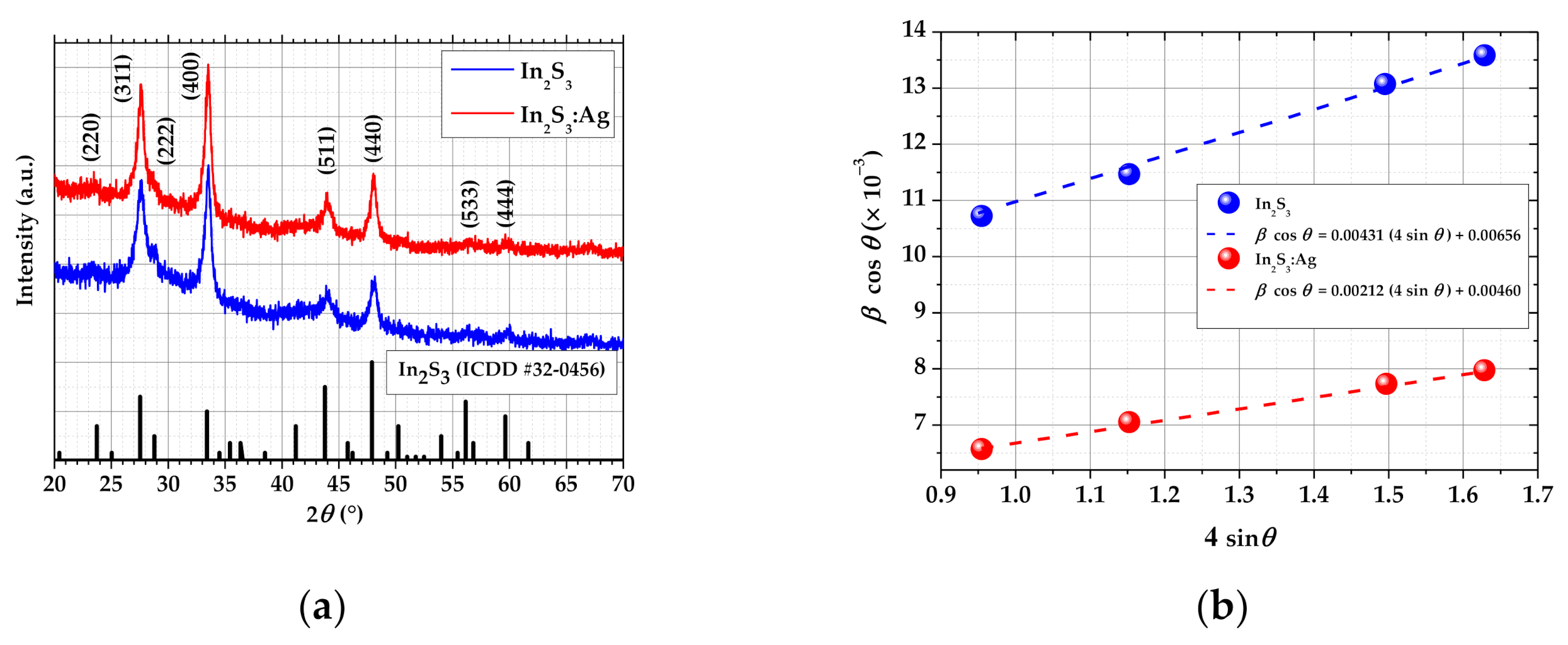
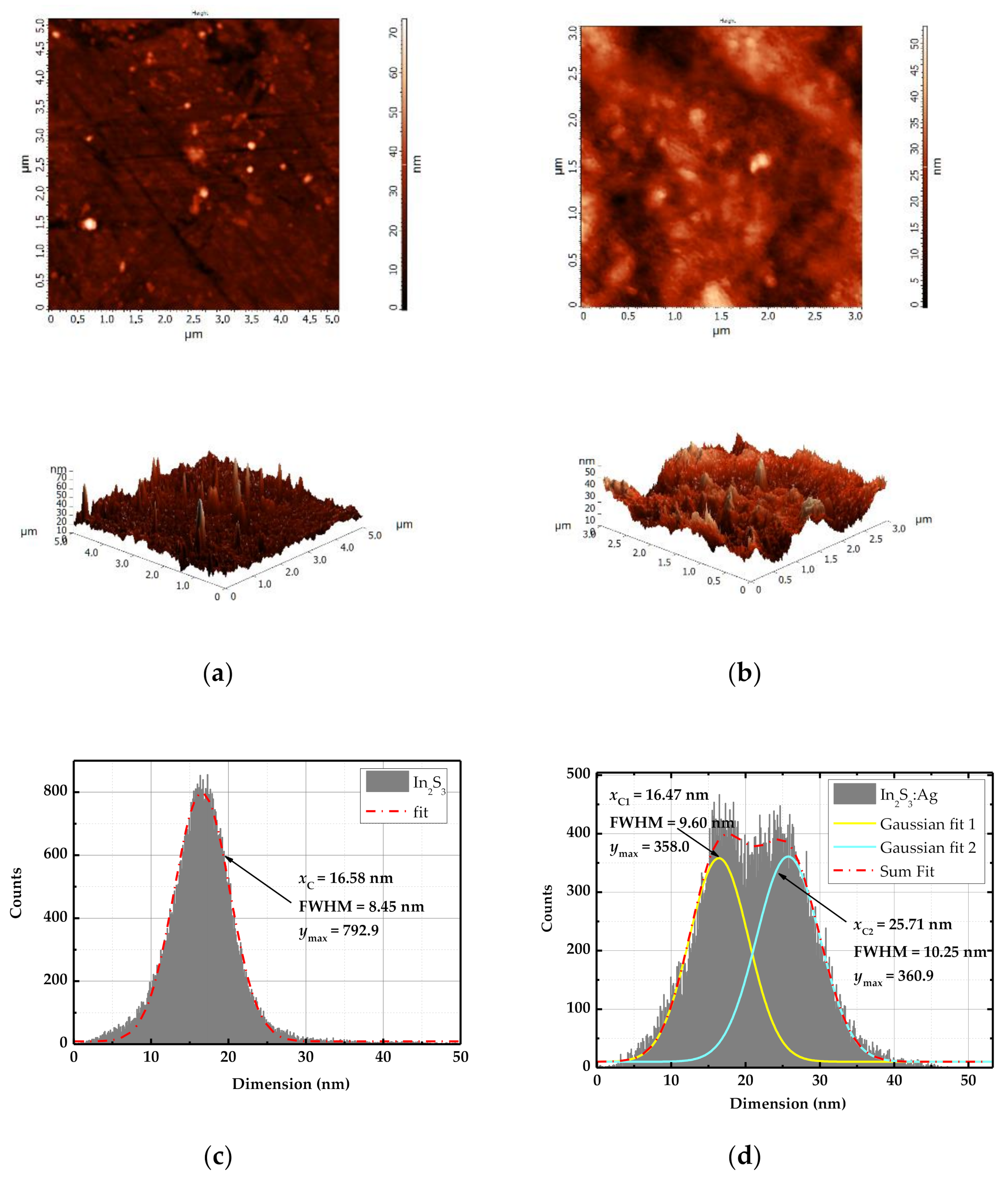
3.1. Structural and Morphological Analysis

The XRD patterns of the films are represented in Figure 1a. It is observed that the Ag doping does not significantly affect the crystallinity. Both films were revealed to be polycrystalline and the XRD patterns suggest that the Ag-doped sample is a solid solution. The In2S3 peaks are indexed in the figure, according to ICDD (International Centre for Diffraction Data) card number 32-0456. The most intense peaks ((311), (400), (511), and (440)) were used to estimate the crystallites’ size by the Williamson–Hall method [45,46]. The obtained data (Figure 1b) show linear trends, and thus, they can be fitted by the Williamson–Hall equation (Equation (2)) [46]:
β cos θ = K λ D + 4 ε sin θ
where β is the full width at half maximum (FWHM) of the referred peaks; θ the correspondent diffraction angle, D , is the crystallite size; λ is the X-ray wavelength; K = 0.9 ; and ε is the microstrain. The slopes of the linear fits ((4.3 ± 0.8) × 10−3 for In2S3 and (2.1 ± 0.2) × 10−3 for In2S3:Ag) correspond to the microstrain, and the crystallite size (around 21 nm for In2S3 and around 30 nm for In2S3:Ag) can be calculated from the intercept of the fit with y-axis.
Figure 2a,b shows the 2D and 3D AFM images of representative scans of the surface of both films (5 μm × 5 μm for In2S3 and 3 μm × 3 μm for In2S3:Ag). From the 3D scans, while the surface of the undoped sample (Figure 3a) reveals a rough surface (RMS (Root Mean Square) roughness 24 nm), the Ag-doped sample surface reveals a combination of roughness (RMS roughness 20 nm) and waviness, with a wavelength of the order of the micrometer. Although this waviness is not observed in the pure In2S3 sample, this surface morphology is certainly resultant of the production technique and of the cooling process. It should not be forgotten that the precursors are sprayed onto the substrates, which are heated at a temperature of 350 °C. Figure 2c,d represent histograms with the size distribution of the diameter of the roughness columns of the as-deposited films, in the scanned areas. The term diameter is used by assuming a circular section for the columns. According to the image processing software, the density of the columns of the doped film is almost three times higher (around 2620 µm−2 for In2S3 and 7280 µm−2 for In2S3:Ag). The column size distribution is also different. While for the sample In2S3, the diameter size of the columns is Gaussian distributed around the 16.6 nm value (FWHM = 8.5 nm) (Figure 2c), in the case of the In2S3:Ag sample, Figure 2d suggests two Gaussian size distributions, centered at 16.5 nm (FWHM = 9.6 nm) and 25.7 nm (FWHM = 10.3 nm). Therefore, the AFM analysis reveals that the roughness is similar for both (slightly lower in the case of the doped sample), but the types of features that cause the roughness are more homogeneous in the case of the undoped sample. In the silver-doped sample, around half of the features are similar to those of the pure In2S3, and the remaining features are around 55% broader.

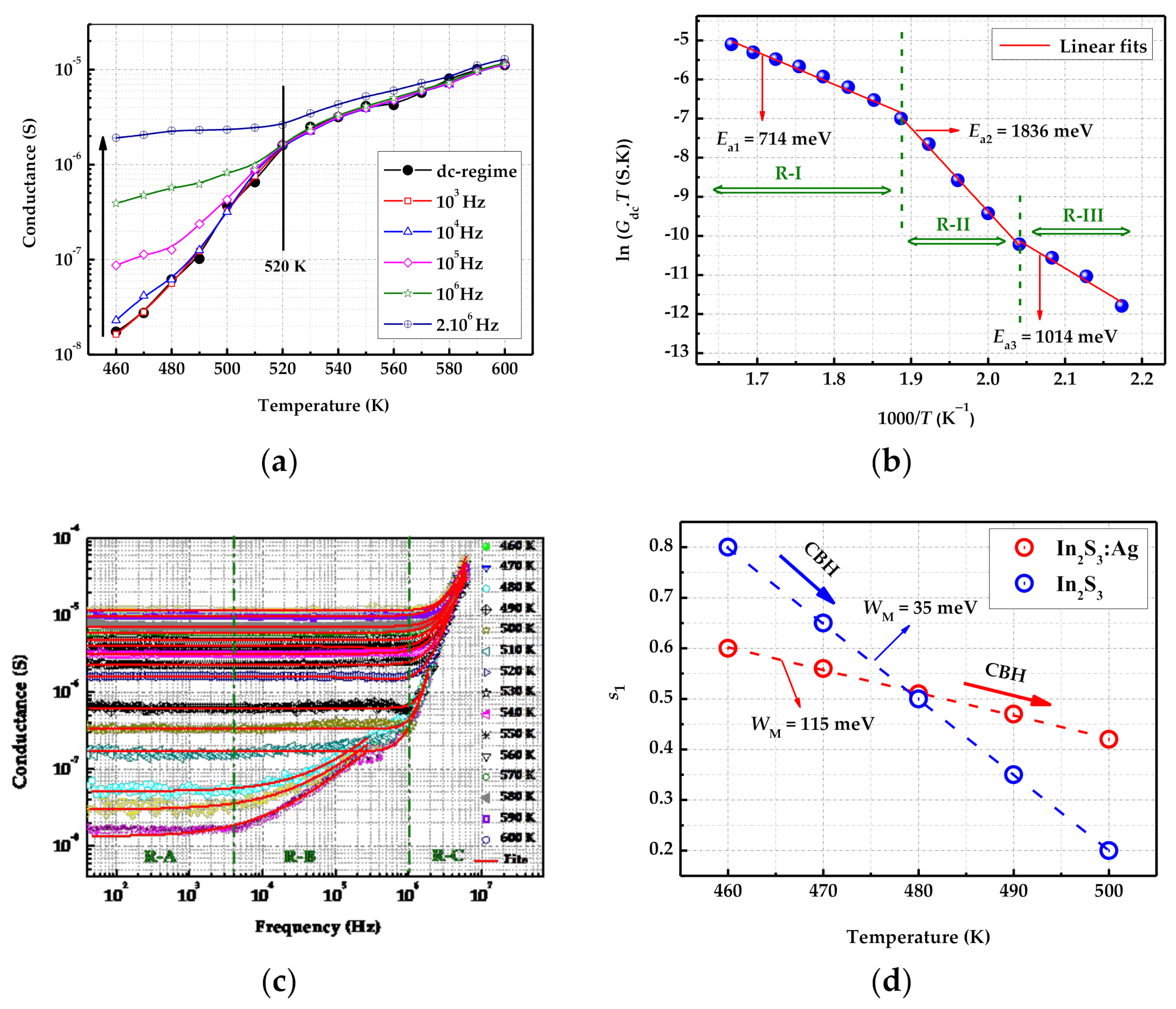
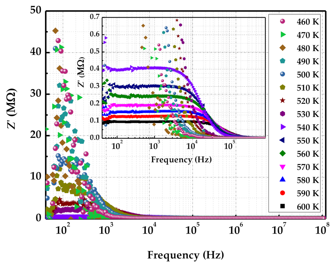
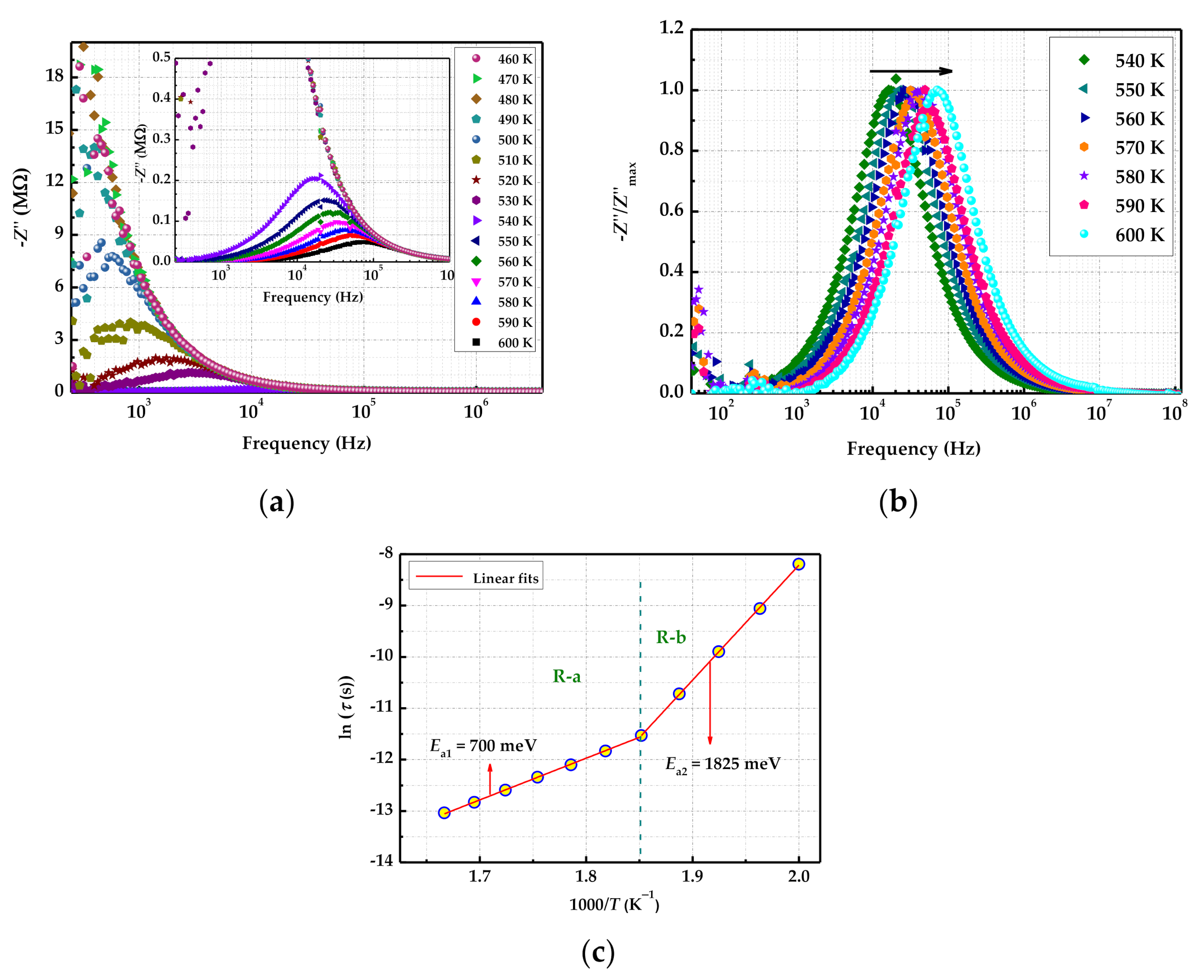
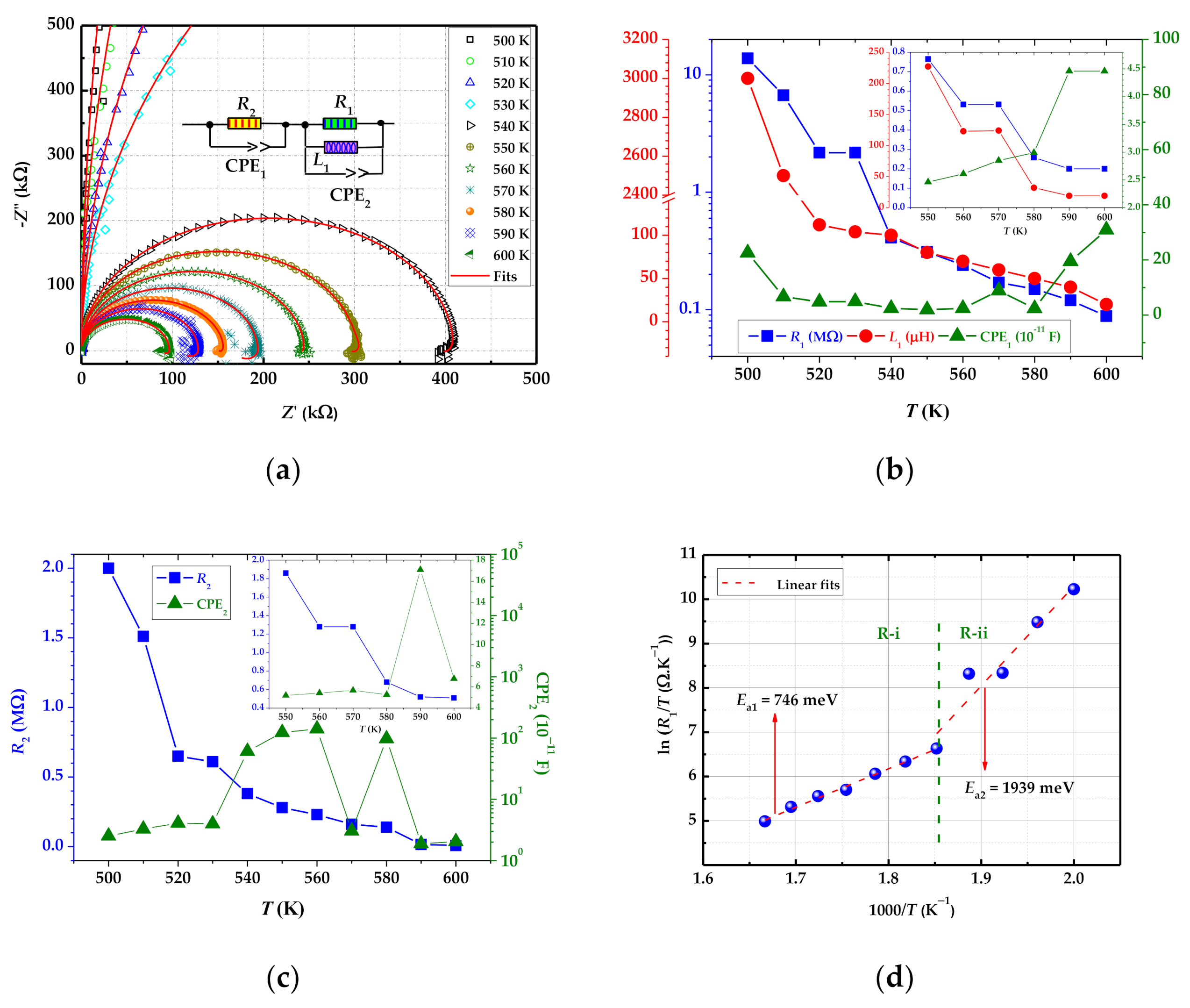
3.2. Electrical Properties

To characterize the films in terms of the electrical conductivity, the direct current (dc) conductance was measured as a function of the temperature. In order to identify the conduction mechanism, the alternating current (ac) conductance was also measured as a function of the temperature. Figure 3a depicts the dependences of dc and ac conductance with the temperature of the In2S3:Ag sample. For both dc and ac measurements, the conductance increases with the temperature, confirming the semiconductor behavior of the material, in the 460 ℃ ≤ T ≤ 600 °C temperature and 1 kHz ≤ f ≤ 2 MHz frequency ranges. The dc conductance of the undoped sample (In2S3) was measured previously [47]. The behavior is also conductive, but the dc conductance is lower, particularly for temperatures above 480 K, where it can be around one order of magnitude lower. The dc conductance ( G dc ) obeys the Arrhenius law [48]. The type of observed variation is reported to happen in disordered and polycrystalline materials [48,49,50,51,52,53,54].
In manganite polycrystalline systems [48,49,50], the semiconductor behavior of the materials is correlated with the activation of a number of conduction processes, such as the small polaron hopping (SPH) and the variable range hopping mechanisms. In theoretical works [51,52,53,54], Mott assumes that the high temperature range of G dc must be investigated in terms of a thermally activated SPH model. To confirm the activation of the SPH mechanism and to calculate the activation energy values in the tested temperature range, the evolution of ln G dc T was plotted as a function of 1000/T (Figure 3b). Three linear fits with different slopes were observed in three temperature ranges. At high temperatures (R-I), the observed linear slope confirms the thermal activation of the SPH mechanism via the activation energy E a 1 = 714 meV. In the second and third temperature ranges, (R-II) and (R-III), the obtained activation energies are E a 2 = 1836 meV and E a 3 = 1014 meV, respectively. The activation energy of the undoped sample (In2S3) obtained by the dc conductance vs. temperature plot for the temperature ranges R-I and R-II, is 999 meV [47]. This result is almost 300 meV higher or more than 800 meV lower than for the case of the In2S3:Ag sample, in the ranges R-I and R-II, respectively.
Besides the semiconductor nature of In2S3:Ag, it is observed, in Figure 3a, that the conductance becomes frequency independent at high temperature (520 K ≤ T ≤ 600 K) and for the frequencies f ≤ 106 Hz. The dc regime is included in this behavior. In this frequency range, the thermally activated SPH process is frequency independent. The aforementioned parameter (frequency) has a strong effect on the conductance variation only in the temperature range 460 K ≤ T ≤ 520 K.
Figure 3c shows the frequency and the temperature dependence of the ac conductance of In2S3:Ag. In the analyzed temperature range, three distinct frequency regions can be observed: a large plateau region (R-A) and two dispersive regions (R-B) and (R-C). This behavior suggests that the variation of the conductance with the angular frequency (ω = 2πf) obeys the Bruce equation (Equation (3)) [55].
G ω = G dc + A 1 ω s 1 + A 2 ω s 2
A1 and A2 are two frequency-independent parameters, and the exponents s1 and s2 are obtained from the fits of the curves of the two dispersive regions, R-B and R-C, respectively, observed in Figure 3c.
The obtained s1 values are presented in Figure 3d, for both doped and undoped samples. This parameter informs about the nature of the activated conduction process in the ac conductance regime [48,49,50]. It can be observed that, in this temperature range, (i) s1 decreases linearly with increasing temperature and (ii) s1 < 1. This behavior indicates a sudden hopping, including translation motion, and, according to theoretical models [48,49,50,51,52,53,54], the nature of the activation is by the correlated barrier hopping (CBH) mechanism. According to the CBH mechanism, the correlation of s1 with the temperature is [56,57]:
s 1 = 1 6 k B T W M + k B T ln ω τ 0 1 6 k B T W M
In this case, W M k B T ln ω τ 0 . In Equation (4), W M is the energy necessary to move one charge carrier from one site to a different site, while τ 0 is a characteristic relaxation time. From the linear slope of the fit of Figure 3d, this energy ( W M ) is around 115 meV, for the doped sample, being around 3.3 times lower for the undoped sample. There are two main reasons for this. One reason is a consequence of the AFM analysis. The larger grain density of the In2S3:Ag sample originates tighter grain boundaries. The other factor is the larger atomic radius of silver atoms relative to indium atoms. This causes a certain degree of cationic disorder in the solid solution of In2S3:Ag. Both factors together contribute to the need of greater energy for charge dislocation. Curiously, Moualhi et al. [48] obtained for the polycrystalline manganite La0.5Ca0.3Ag0.2MnO3 a similar result, in terms of activation mechanism (CBH) and activation energy ( W M = 74 meV). In the second dispersive region (R-C), it was found that the frequency exponent s2 is higher than unity and varying in the range 1.5 < s2 < 2. This indicates that the transport of charge, in the region of high frequencies (R-C), occurs via localized hopping between neighboring sites. The same behavior was observed recently by Hizi et al. in polycrystalline La0.9Sr0.1MnO3 [50].
Figure 4 illustrates the frequency dependence of the real part of the impedance (Z’) in the studied temperature range. At low frequencies and for the 460 K ≤ T ≤ 530 K temperature range, Z’ exhibits high impedance values, in the order of tens of MΩ. For the highest temperature range (540 K ≤ T ≤ 600 K), the impedance monotonously decreases with increasing temperature. The frequency at which the impedance becomes significant generally increases with the temperature. This is better observed in the inserted graph of Figure 4. In polycrystalline materials such as manganites [49], the Z’ decrease with the temperature was explained by the drop in the density of trapped charges and the increase of charge carriers’ mobility. At higher frequencies, Z’ values shift to small values confirming the presence of space charge in the sample.
Figure 5a,b shows the frequency dependence of the imaginary part of the impedance (Z’’) in the tested temperature range (460 K ≤ T ≤ 600 K). Each curve is characterized by one peak at a specific relaxation frequency ( f r ). The observed peak is a signature of a dielectric relaxation of the compound. In Figure 5b, the ratio of the imaginary component of the impedance to the maximum of the imaginary component of impedance is represented, as a function of the frequency, for the 540 K ≤ T ≤ 600 K temperature range. One can observe that the peak shifts to higher frequencies for higher temperatures, which can be a consequence of the decline of the resistive behavior with increasing temperature. Figure 5c presents the evolution of the relaxation time (τ) as a function of the temperature for the Ag-doped In2S3. The variation of relaxation time obeys the Arrhenius equation (Equation (5)):
τ = τ 0 e E a k B T
τ 0 is a characteristic relaxation time, k B is the Boltzmann constant, and E a is the activation energy. This energy is obtained from the linear slope of ln τ vs. 1000/T. For this particular case (the system In2S3:Ag), two different regimes (R-a and R-b) occur and, as a consequence, two different values for the activation energy are obtained: E a 1 = 700 meV ( τ 0 = 2.8 × 10 12 s) and E a 2 = 1825 meV ( τ 0 = 9.6 × 10 24 s). The inferred values of the activation energy obtained from the impedance analysis are different when compared to those determined by the dc conductance study. This result confirms the incoherence between the conduction process and relaxation phenomena, signifying that they may have different origins. The activation energy of the undoped indium sulfide, obtained from relaxation frequency, is 924 meV [58], and it is similar to the one obtained by the dc conductivity approach previously referred (926 meV).
The Nyquist diagram of Z’’ as function of Z’ is frequently employed to correlate the microstructure of the material with its ac electrical properties. Figure 6a shows the Nyquist diagram of the In2S3:Ag system, at different temperatures. The Nyquist diagram of the undoped sample is represented in a previous work [58]. By increasing the temperature, the intensity of the arcs decreases, confirming thermal activation of the processes. At low frequencies, the observed arc is attributed to the grain boundary conduction [49]; however, at higher frequencies, the transport properties of the studied film are governed by the grain contribution. In this context, ZView2 software was used to fit the curves and build the equivalent electrical circuit model. The obtained equivalent for both system (In2S3 [58] and In2S3:Ag) circuits consists of two serial components. The first one is composed by three parallel elements, an inductor ( L 1 ), a resistor ( R 1 ), and a constant phase element (CPE1). The second component combines a resistor ( R 2 ) in parallel with another constant phase element (CPE2). For the case of In2S3:Ag film, the inductance effect ( L ) contained in the equivalent circuit is generally associated with specific energy adsorption and electro-crystallization processes at an electrode. This absorption process is reported by Chung [59].
It is observed that R 1 of the equivalent circuit correspondent to In2S3:Ag exhibits high values at lower temperatures, of the order of the MΩ, or even tens of MΩ for T = 500 K, suggesting the important role of the grain boundary contributions on the transport of charge carriers. For T ≥ 550 K, R 1 for the undoped and Ag-doped samples are similar but always lower for the doped sample, as expected. The constant phase element (CPE1) impedance is correlated with the angular frequency, by Equation (6):
1 Z C P E = Q 0 j ω β
where Q 0 is a constant, independent of the frequency, the angular frequency ( ω = 2 π f ), and depending on the values of the exponent β; CPE is a capacitor for β = 1 , a resistor for β = 0 , and an inductor for β = 1 . For CPE1, it was found that β ≥ 0.94, indicating the resemblance with a capacitor.
For the case of the other component of the equivalent circuit, a similar behavior for the resistance (high values at lower temperatures) is observed in Figure 6c. In the present study, the charge transfer resistance response represents the contribution of the grains on the electrical transport phenomena of the thin film. This resistance is represented by R 2 . According to Sørensen et al. [60], the decrease of the charge transfer resistance leads to the increase of the characteristic frequency of the corresponding semicircle. This observation is in good agreement with the results presented herein. For CPE2, β 0.95 was obtained (capacitor resemblance).
Figure 6d shows the evolution of ln R 1 T as a function of the inverse of the temperature. From the linear slope, the deduced activation energies are E a 1 = 746 and E a 2 = 1939 meV. The activation energies obtained from the dc conductance data and those obtained from grain boundary resistances do not show correlation. This indicates that in the Ag-doped film case, the transport phenomena and the relaxation phenomena do not have the same origin. The activation energy for the undoped sample calculated from a ln R 1 T vs. T plot is 939 meV [58]. Consequently, it is verified that for undoped In2S3 the activation energy is similar regardless of the used method of calculation (926 meV, from the conductance plot method, and 924 meV for the relaxation frequency method).

3.3. Photocatalytic Activity

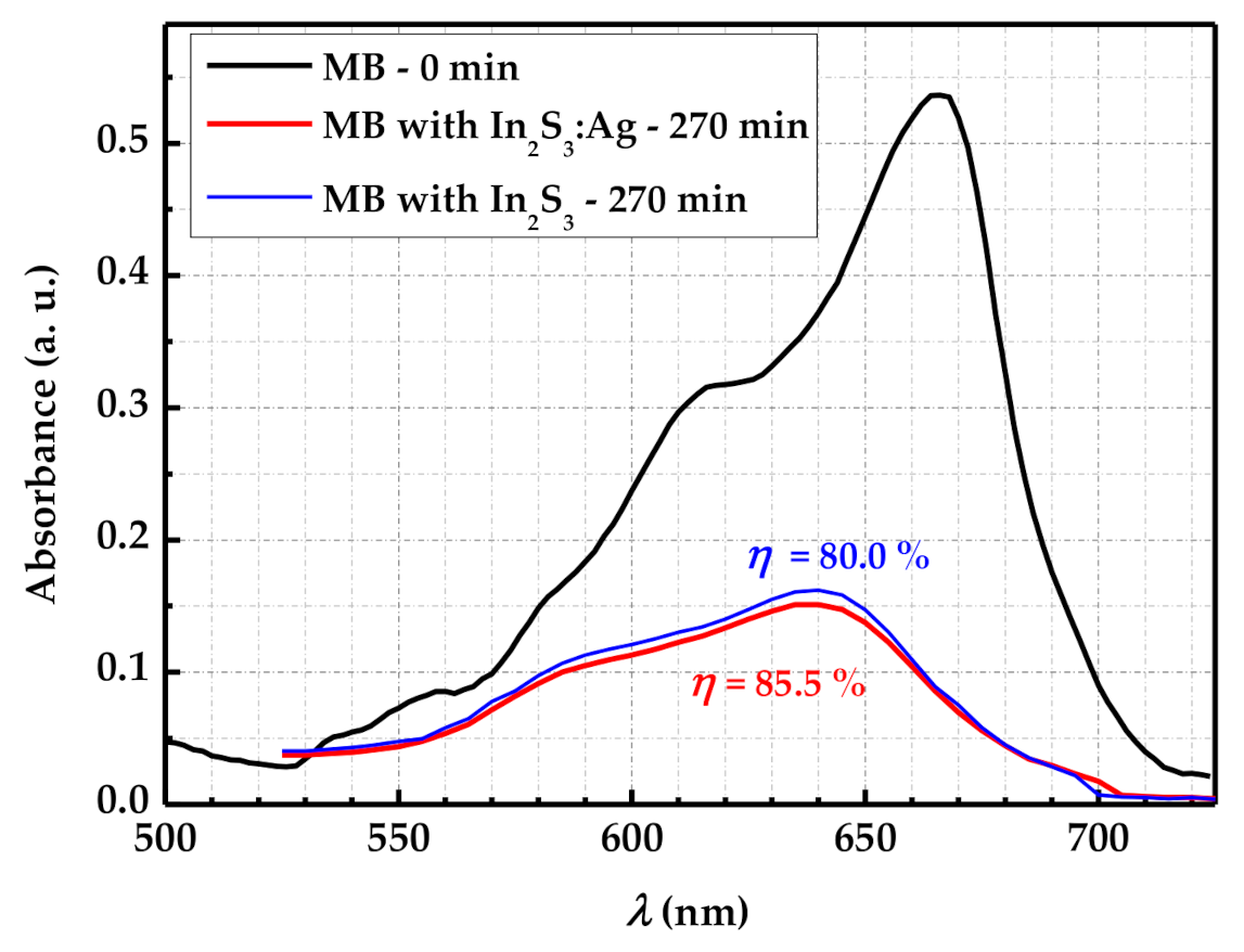
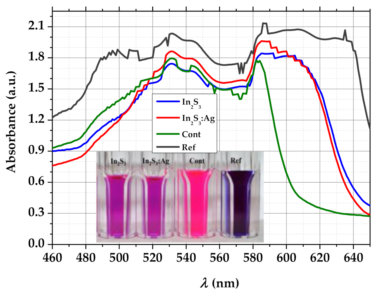
3.3.1. Absorption Analysis of MB Solution and Photodegradation Efficiency

Figure 7 shows the absorbance spectra of an aqueous solution of methylene blue (MB) under visible-light irradiation in three different situations: as-prepared solution (0 min of exposure), after 270 min irradiation in the presence of an In2S3:Ag sample, and after 270 min irradiation in the presence of an In2S3 undoped sample. The result of the as-prepared solution reveals the existence of two major absorbance peaks at λ ≈ 665 nm, due to the presence of monomers MB+, and at λ ≈ 610 nm, related to the presence of dimers (MB+)2 [61]. Compared to the as-prepared solution, after irradiation, the absorption peaks progressively shift toward the blue direction. The highest-intensity peak shifts from λ ≈ 665 to λ ≈ 639 nm. This behavior was explained by the hypsochromic effect [62]. The presence of the indium sulfide samples in the MB solution, under visible light irradiation during 270 min, causes a huge decrease of the absorbance for all the visible-wavelength range. This decrease is particularly measurable in the large absorption peak (λ = 665 nm), decreasing from A ≈ 0.536, for the as-prepared solution, to A ≈ 0.162 and A ≈ 0.151, after irradiation in the presence of the undoped In2S3 and In2S3:Ag, respectively. The absorbance intensity ratio of the two peaks ( A λ 665 A λ 610 ) decreases from around 1.68 to around 1.46, thus suggesting that the photodegradation of the monomers is higher than the one of the dimers [63]. The simultaneous decrease of the absorption intensities and the slight blue shifting of the monomers bands is due to the N-demethylated degradation concomitantly with the degradation of phenothiazine [64]. In these conditions, the photodegradation efficiency of the MB in the presence of In2S3:Ag exhibits high efficiency ( η In 2 S 3 = 80.0 % and η In 2 S 3 : Ag = 85.5 % ). This good result may be due to the good crystal quality and, particularly, to the relatively high roughness (large effective surface area) of the films.
The photodegradation capacity of the Ag-doped In2S3 thin film is ~6% more efficient than that of the reference In2S3 sample, which could be due to Ag+ ions entering the In2S3 lattice (Ag+ and In3+ have roughly the same ionic radii, namely 67 vs. 62 pm) and creating interstitial and/or substitutional doping sites. This generates an increased concentration of charge carriers, which determines a higher electrical conductance and photocatalytic activity than that for undoped In2S3 [65]. Moreover, the presence of Ag+ could generate conductance pathways on the surface of the film. This could explain the lower values for the WM energy for the doped sample.

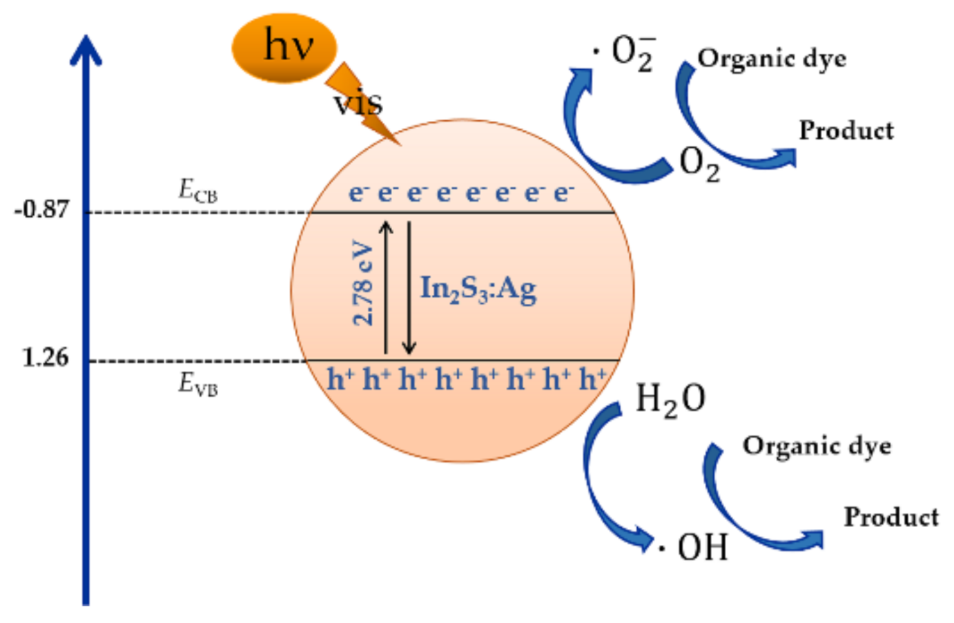
3.3.2. Photodegradation Mechanism

The electrical properties of In2S3:Ag have an important role regarding the photodegradation of MB. To better understand the photodegradation mechanism of the MB in the presence of In2S3:Ag, the conduction band ( E CB ) and valence band ( E VB ) energies of β-In2S3:Ag were theoretically estimated using the Mulliken equation [66]:
E CB = χ E c 0.5 E g
E VB = χ E c + 0.5 E g
E g , E c , and χ represent the band gap energy of In2S3:Ag (∼2.78 eV), the free electrons energy on the hydrogen scale (∼4.5 eV) and the electronegativity of In2S3 (∼4.71 eV), respectively [67]. The estimated values of E CB and E VB are −0.87 and 1.26 eV, respectively. As shown in Figure 8, the E CB value of In2S3 is more negative than the energy value of O 2/ O 2 (0.28 eV).
Furthermore, under irradiation with visible light, the photogenerated electrons have the ability to react with the molecular O2 adsorbed on the surface of the catalyst, to generate the superoxide radical anion · O 2 [68]. Moreover, the E VB value of In2S3 is less positive than the energy value of OH/OH · (2.38 eV) and ⋅OH/H2O (2.8 eV), which indicates that the photogenerated holes can be captured by H2O and produce hydroxyl radicals OH · [69,70]. The band gap energy obtained for the compound is equal to 2.78 eV, and it is in good agreement with literature values [15,44]. We note this when the decrease of the optical band gap energy is related with the photovoltaic parameter improvement. Indeed, it shows that this radical OH · has a markedly greater oxidizing power than those of several other commonly used oxidants. Because of this, it can degrade many organic compounds and transform them into carbon dioxide. On the other hand, the radical mechanism only requires low activation energy. This technique allows it to operate at moderate temperatures. Due to their high oxidizing power in an acidic environment, OH · radicals can react with organic compounds to produce radicals (R · or ROO · ). Organo peroxyl radicals decompose to generate by-products ( · HO2/ · O2). However, the photogenerated holes are able to immediately oxidize the MB dye molecules into the final products [71]. The auto-decomposition of H2O2 into O2 and H2O and the scavenging of hydroxyl radicals by H2O2 are well explained by the Reactions (9) and (10):
2 H 2 O 2 O 2   +   2 H 2 O
H 2 O 2   +   · OH   · HO 2   +   H 2 O
The scavenging character of H2O2 reduces the efficiency of the treatment through the consumption of hydroxyl radicals leading to the formation of · HO2, which has a negligible contribution in the Fenton process.
H 2 O · OH   + H + + e
· OH   1 2 O 2   +   H + + e
Dyes     · OH CO 2   +   H 2 O
This mechanism translates the photocatalytic activity of the cationic dye (MB), using hydroxyl radicals, corresponding to the enhancement of MB removal. Similar results were reported by Chen et al. [72].
Generally, a comparison of the photocatalytic activity of different composite systems mentioned in the reference literature is difficult, due to the different photocatalysis experimental conditions, dye types, and concentration. It can be said that roughly similar photocatalytic activity (~80%) was observed for crystal violet photodegradation by In2S3 nanocrystals [73], 80–85% for MB (In2S3-n via hydrothermal synthesis) [74] and ~86% for MB (In2S3 synthesized by chemical bath deposition) [75], under visible-light irradiation. Composite photocatalytic heterostructures exhibit various efficiencies. For example, TiO2:In2S3 has a visible light photodegradation efficiency of 50–70% for orange II dye [76], In2S3/ZnFe2O4 exhibits maximum photodegradation efficiencies of 85–90% [77], and Cu2FeSnS4/In2S3 shows a photodegradation efficiency of ~80% for MB [78].

3.4. Antibacterial Activity

Figure 9 shows the absorbance spectra and the photographic image of the test solutions, three of which contained Pseudomonas aeruginosa (Cont., In2S3, and In2S3:Ag), after the period of incubation and dye addition. Both the color and the spectra of the solutions revealed that the incubation period induced different changes in the three solutions. If the color of a solution is pink, it means that its antibacterial activity is weak. The only pink solution is the control (Cont.), the one in which resazurin was added without the presence of In2S3:Ag or In2S3 samples. Clearly, in this solution, there is no antibacterial activity. As mentioned previously, resazurin is reduced to resorufin (pink hue) by the aerobic respiration of metabolically active cells, in this case, the Pseudomonas aeruginosa colonies. As expected, the Ref sample does not exhibit any change from the dark-purple hue, since there are no active colonies of cells in the solution. The color of the solutions containing the samples (In2S3:Ag and In2S3) is a mixture of pink and purple, thus inferring that the growth and/or cell viability was hindered to some extent, but not entirely, by the In2S3:Ag and In2S3 films.
Analyzing the absorption spectrum of the control solution from Figure 9, the sharp peak at λ ≈ 580 nm is close to the peak of resorufin ( λ   =   573 nm), meaning that the bacterial colonies developed, revealing a solution with no antibacterial activity, as was expected [79]. The absorbance spectrum of the solution containing the sample with the In2S3:Ag film reveals a different shape. For λ   >   580 nm an absorption band is noticed that goes until λ ≈ 630 nm, which includes the wavelength of the maximum absorption peak of resazurin ( λ   =   605 nm). This behavior confirms that the investigated thin films can be considered as antibacterial materials, to some extent. Considering that the photodegradation efficiencies exhibited by the In2S3:Ag and In2S3 films are somewhat similar, the fact that the antibacterial capacity is also similar was expected. However, one has to consider the fact that the doped sample contains a relatively low quantity of silver, which is located not only on its surface (where the reduction processes would take place), but also in the bulk of the In2S3 coating.
As it has been found in other studies from the reference literature, the reactive oxygen radical species, such as the superoxide anion or the hydroxyl radical, can interact with the cell wall of the bacteria, disrupting it [80,81]. The generation of these active species can be correlated with the photocatalytic activity of the film. Since the photocatalytic efficiency of the In2S3:Ag film was ~85%, it can be concluded that this relatively high efficiency could be responsible for the antibacterial effect. Another factor that influences the antibacterial effect is the roughness of the film. The nanostructured patterns responsible for the film’s roughness and waviness (Figure 2) increase the specific surface of the photoactive surface, generating a higher number of oxidative radicals. The antibacterial effect also depends on the nanotopography of the surface. A higher number of nanopatterns could be responsible for the mechanical piercing of the bacterial cell wall or for contacting the cell wall and disrupting the metabolic and reproductive activity of the bacteria [82]. The correlation between the photocatalysis-related parameters and nanopatterning of the surface on the antibacterial effect will be discussed in more detail in a future study.

4. Conclusions

Indium sulfide films, with or without silver doping, deposited by spray pyrolysis are polycrystalline, with the crystallite sizes around 20 nm (pure indium sulfide) and 32 nm (silver-doped indium sulfide). Structurally, silver is incorporated as a solid solution. Electrical characterization confirms the films as semiconductors; however, the Ag doping leads to an increase in conductivity. Alternating current conductance curves for different frequencies and temperatures have been fitted according to the Bruce equation. The study of alternating current conductance reveals that the small polaron hopping process is thermally activated at high temperatures. The variation of the ac conductance with the frequency (for several temperature values) reveals two dispersive regimes, one of them explained by the activation of a correlated barrier hopping process and the other, in the high-frequency region, indicates that the transport of charge occurs via localized hopping between neighboring sites. Impedance results confirm the importance of the grain and grain boundaries contributions in the transport phenomena of the thin film. The structure of the films, their relatively high roughness and electrical characteristics, positively influence the photocatalytic activity (to photodegrade methylene blue) and their antibacterial characteristics, tested against Pseudomonas aeruginosa. Particularly in the case of the photodegradation, the Ag doping slightly increases the efficiency of the process, reaching 85.5%. Future studies will allow correlation of the photocatalysis-related parameters and nanopatterning of the surface on the antibacterial effect.

Author Contributions

Conceptualization, B.T., Y.M. and N.B.; methodology, B.T. and N.B.; software, B.T. and M.K.; validation, N.B. and S.A.; formal analysis, Y.M., M.K., C.C., I.G., D.C. and D.P.; investigation, B.T., Y.M., M.K., I.G., D.C., C.C. and D.P.; resources, L.C., C.M., D.C. and N.B.; data curation, B.T. and Y.M.; writing—original draft preparation, B.T.; writing—review and editing, L.C., C.M. and D.C.; visualization, N.B.; supervision, C.M., L.C., N.B. and S.A.; project administration, N.B.; funding acquisition, N.B., L.C., C.M. and D.C. All authors have read and agreed to the published version of the manuscript.

Funding

Part of this work was supported by the Portuguese Foundation for Science and Technology (FCT) in the framework of the Strategic Funding UIDB/04650/2020”. D.C. and I.G. acknowledge the structural funds project PRO-DD (POS-CCE, O.2.2.1., ID123, SMIS 2637, ctr. no 11/2009) for providing some of the infrastructure used in this work. Part of this work was supported by a grant of the Romanian Ministry of Education and Research, CNCS - UEFISCDI, project number PN-III-P1-1.1-TE-2019-1209, within PNCDI III.

Institutional Review Board Statement

Not applicable.

Informed Consent Statement

Informed consent was obtained from all subjects involved in the study.

Data Availability Statement

The data presented in this study are available on reasonable request from the corresponding author.

Acknowledgments

B.T. and L.C. acknowledge the support given by P. Martins and S. Lanceros-Mendez, of the Physics Center of Minho and Porto Universities - CF-UM-UP on the electrical properties equipment and C. Vázquez-Vázquez by support with the EDX measurements.

Conflicts of Interest

The authors declare no conflict of interest.

References

  1. Liu, Y.; Cheng, M.; Liu, Z.; Zeng, G.; Zhong, H.; Chen, M.; Zhou, C.; Xiong, W.; Shao, B.; Song, B. Heterogeneous Fenton-like catalyst for treatment of rhamnolipid-solubilized hexadecane wastewater. Chemosphere 2019, 236, 124387. [Google Scholar] [CrossRef]
  2. Gong, X.; Huang, D.; Liu, Y.; Zeng, G.; Wang, R.; Wei, J.; Huang, C.; Xu, P.; Wan, J.; Zhang, C. Pyrolisis and reutilization of plant residues after phytoremediation of heavy metals contaminated sediments: For heavy metals, stabilization and dye absorption. Bioresour. Technol. 2018, 253, 64–71. [Google Scholar] [CrossRef] [PubMed]
  3. Houas, A.; Lachheb, H.; Ksibi, M.; Elaloui, E.; Guillard, C.; Herrmann, J.M. Photocatalytic degradation pathway of methylene blue in water. Appl. Catal. B 2001, 31, 145–157. [Google Scholar] [CrossRef]
  4. Kuriakose, S.; Satpati, B.; Mohapatra, S. Enhanced photocatalytic activity of Co doped ZnO nanodisks and nanorods prepared by a facile wet chemical method. Phys. Chem. Chem. Phys. 2014, 16, 12741–12749. [Google Scholar] [CrossRef] [PubMed]
  5. Trandafilović, L.V.; Jovanović, D.J.; Zhang, X.; Ptasińska, S.; Dramićanin, M.D. Enhanced photocatalytic degradation of methylene blue and methyl orange by ZnO:Eu nanoparticles. Appl. Catal. B 2017, 203, 740–752. [Google Scholar] [CrossRef] [Green Version]
  6. Jiang, Z.-J.; Liu, C.-Y.; Sun, L.-W. Catalytic properties of silver nanoparticles supported on silica spheres. J. Phys. Chem. B 2005, 109, 1730–1735. [Google Scholar] [CrossRef]
  7. Liu, T.; Li, Y.; Du, Q.; Sun, J.; Jiao, Y.; Yang, G.; Wang, Z.; Xia, Y.; Zhang, W.; Wang, K.; et al. Adsorption of methylene blue from aqueous solution by graphene. Colloids Surf. B Biointerfaces 2012, 90, 197–203. [Google Scholar] [CrossRef]
  8. Rehman, M.S.U.; Kim, I.; Han, J.-I. Adsorption of methylene blue dye from aqueous solution by sugar extracted spent rice biomass. Carbohydr. Polym. 2012, 90, 1314–1322. [Google Scholar] [CrossRef]
  9. Wang, Z.; Huang, B.; Dai, Y.; Qin, X.; Zhang, X.; Wang, P.; Liu, H.; Yu, J. Highly photocatalytic ZnO/In2O3 heteronanostructures synthesized by a coprecipitation method. J. Phys. Chem. C 2009, 113, 4612–4617. [Google Scholar] [CrossRef]
  10. Zhu, C.; Liu, C.; Fu, Y.; Gao, J.; Huang, H.; Liu, Y.; Kang, Z. Construction of CDs/CdS photocatalysts for stable and efficient hydrogen production in water and seawater. Appl. Catal. B Environ. 2019, 242, 178–185. [Google Scholar] [CrossRef]
  11. Zhu, X.; Lin, Y.; Sun, Y.; Beard, M.C.; Yan, Y. Lead-halide perovskites for photocatalytic α-alkylation of aldehydes. J. Am. Chem. Soc. 2019, 141, 733–738. [Google Scholar] [CrossRef] [PubMed]
  12. Luo, Y.-H.; Dong, L.-Z.; Liu, J.; Li, S.-L.; Lan, Y.-Q. From molecular metal complex to metal-organic framework: The CO2 reduction photocatalysts with clear and tunable structure. Coord. Chem. Rev. 2019, 390, 86–126. [Google Scholar] [CrossRef]
  13. Zeng, D.; Zhou, T.; Ong, W.-J.; Wu, M.; Duan, X.; Xu, W.; Chen, Y.; Zhu, Y.-A.; Peng, D.-L. Sub-5 nm ultra-fine FeP nanodots as efficient co-catalysts modified porous g-C3N4 for precious-metal-free photocatalytic hydrogen evolution under visible light. ACS Appl. Mater. Interfaces 2019, 11, 5651–5660. [Google Scholar] [CrossRef] [PubMed]
  14. Rasool, S.; Saritha, K.; Ramakrishna Reddy, K.T.; Raveendranath Reddy, K.; Bychto, L.; Patryn, A.; Maliński, M.; Tivanov, M.S.; Gremenok, V.F. Optical properties of thermally evaporated In2S3 thin films measured using photoacoustic spectroscopy. Mater. Sci. Semicond. Process. 2017, 72, 4–8. [Google Scholar] [CrossRef]
  15. Buecheler, S.; Guettler, D.; Chirila, A.; Verma, R.; Müller, U.; Niesen, T.P.; Palm, J.; Tiwari, A.N. Ultrasonically sprayed indium sulfide buffer layers for Cu(In,Ga)(S,Se)2 thin-film solar cells. Thin Solid Films 2009, 517, 2312–2315. [Google Scholar] [CrossRef]
  16. Barreau, N.; Marsillac, S.; Albertini, D.; Bernède, J.C. Structural, optical and electrical properties of β-In2S3-3xO3x thin films obtained by PVD. Thin Solid Films 2002, 403, 331–334. [Google Scholar] [CrossRef]
  17. Pistor, P.; Merino Álvarez, J.M.; León, M.; di Michiel, M.; Schorr, S.; Klenka, R.; Lehmann, S. Structure reinvestigation of α-, β- and γ-In2S3. Acta. Cryst. B Struct. Sci. Cryst. Eng. Mater. 2016, 72, 410–415. [Google Scholar] [CrossRef] [Green Version]
  18. Bchiri, Y.; Tiss, B.; Bouguila, N.; Souissi, R.; Kraini, M.; Vázquez-Vázquez, C.; Khirouni, K.; Alaya, S. Electrical investigation of sprayed In2S3 film. Mater. Sci. Semicond. Process. 2021, 121, 105294. [Google Scholar] [CrossRef]
  19. Galarza-Gutierrez, U.; Albor-Aguilera, M.L.; Gonzalez-Trujillo, M.A.; Hernandez-Vasquez, C.; Ortega-Cardenas, J.A.; Flores-Marquez, J.M.; Cruz-Gandarilla, F.; Ramírez-Rosales, D.; Mendoza-Pérez, R.; Rueda-Morales, G. Incorporation of an efficient β-In2S3 thin film as window material into CdTe photovoltaic devices. Mat. Res. Express 2019, 6, 125510. [Google Scholar] [CrossRef]
  20. Soni, P.; Raghuwanshi, M.; Wuerz, R.; Berghoff, B.; Knoch, J.; Raabe, D.; Cojocaru-Mirédin, O. Role of elemental intermixing at the In2S3/CIGSe heterojunction deposited using reactive RF magnetron sputtering. Sol. Energy Mater. Sol. Cells 2019, 195, 367–375. [Google Scholar] [CrossRef]
  21. Xu, H.; Wang, Y.; Dong, X.; Zheng, N.; Ma, H.; Zhang, X. Fabrication of In2O3/In2S3 microsphere heterostructures for efficient and stable photocatalytic nitrogen fixation. Appl. Catal. B Environ. 2019, 257, 117932. [Google Scholar] [CrossRef]
  22. Uma, H.B.; Ananda, S.; Rai, V.R. Synthesis and characterization of In2S3 nanoparticles by electrochemical method: Evaluation of its performance in photo-assisted degradation of indigo carmine dye, antibacterial and antimitotic activity studies. Int. J. Nanotechnol. Appl. 2017, 7, 1–16. [Google Scholar] [CrossRef]
  23. Kamoun, N.; Belgacem, S.; Amlouk, M.; Bennaceur, R.; Bonnet, J.; Touhari, F.; Nouaoura, M.; Lassabatere, L. Structure, surface composition, and electronic properties of β-In2S3 and β-In2−xAlxS3. J. Appl. Phys. 2001, 29, 2766. [Google Scholar] [CrossRef]
  24. Faller, P.; Kienzler, K.; Krieger-Liszkay, A. Mechanism of Cd2+ toxicity: Cd2+ inhibits photoactivation of Photosystem II by competitive binding to the essential Ca2+ site. Biochimica Biophysica Acta (BBA) Bioenerg. 2005, 1706, 158–164. [Google Scholar] [CrossRef] [PubMed] [Green Version]
  25. Barreau, N. Indium sulfide and relatives in the world of photovoltaics. Sol. Energy 2009, 83, 363–371. [Google Scholar] [CrossRef]
  26. Timoumi, A.; Bouzouita, H.; Kanzari, M.; Rezig, B. Fabrication and characterization of In2S3 thin films deposited by thermal evaporation technique. Thin Solid Films 2005, 480–481, 124–128. [Google Scholar] [CrossRef]
  27. Barreau, N.; Mokrani, A.; Couzinié-Devy, F.; Kessler, J. Bandgap properties of the indium sulfide thin-films grown by co-evaporation. Thin Solid Films 2009, 517, 2316–2319. [Google Scholar] [CrossRef]
  28. Allsop, N.A.; Schönmann, A.; Muffler, H.-J.; Bär, M.; Lux-Steiner, M.C.; Fisher, C.-H. Spray-ILGAR indium sulfide buffers for Cu(In,Ga)(S,Se)2 solar cells. Prog. Photovolt. Res. Appl. 2005, 13, 607–616. [Google Scholar] [CrossRef]
  29. Naghavi, N.; Spiering, S.; Powalla, M.; Cavana, B.; Lincot, D. High-efficiency copper indium gallium diselenide (CIGS) solar cells with indium sulfide buffer layers deposited by atomic layer chemical vapor deposition (ALCVD). Prog. Photovolt. Res. Appl. 2003, 11, 437–443. [Google Scholar] [CrossRef]
  30. Li, Z.; Tao, X.; Wu, Z.; Zhang, P.; Zhang, Z. Preparation of In2S3 nanopraricle by ultrasonic dispersion and its tribology property. Ultrason. Sonochem. 2009, 16, 221–224. [Google Scholar] [CrossRef]
  31. Lee, W.; Baek, S.; Mane, R.S.; Todkar, V.V.; Egorova, O.; Chae, W.-S.; Lee, S.-H.; Han, S.-H. Liquid phase deposition of amorphous In2S3 nanorods: Effect of annealing on phase change. Curr. Appl. Phys. 2009, 9, S62–S64. [Google Scholar] [CrossRef]
  32. Mari, B.; Mollar, M.; Soro, D.; Henriquez, R.; Schrebler, R.; Gómez, H. Electrodeposition of In2S3 thin films onto FTO substrate from DMSO solution. Int. J. Electrochen. Sci. 2013, 8, 3510–3523. [Google Scholar]
  33. Portillo-Vélez, N.S.; Bizarro, M. Sprayed pyrolyzed ZnO films with nanoflake and nanorod morphologies and their photocatalytic activity. J. Nanomater. 2016, 2016, 5981562. [Google Scholar] [CrossRef] [Green Version]
  34. Raj Mohamed, J.; Amalraj, L. Effect of precursor concentration on physical properties of nebulized spray deposited In2S3 thin films. J. Asian Ceram. Soc. 2016, 4, 357–366. [Google Scholar] [CrossRef] [Green Version]
  35. Zheng, Z.; Yu, J.; Cheng, S.; Lai, Y.; Zheng, Q.; Pan, D. Investigation of structural, optical and electrical properties of Cu doped β-In2S3 thin films. J. Mater. Sci. Mater. Electron. 2016, 27, 5810–5817. [Google Scholar] [CrossRef]
  36. Rodríguez-Hernández, P.E.; Quiñones-Galván, J.G.; Marasamy, L.; Morales-Luna, M.; Santos-Cruz, J.; Arias-Cerón, J.S.; Zelaya-Angel, O.; de Moure-Flores, F. Optoelectronic properties of undoped and Al, B and Ga-doped In2S3 thin films grown by CBD on flexible PET/ITO substrates. Mater. Sci. Semicond. Process. 2019, 103, 104600. [Google Scholar] [CrossRef]
  37. Mathew, M.; Jayakrishnan, R.; Ratheesh Kumar, P.M.; Sudha Kartha, C.; Vijayakumar, K.P. Anomalous behavior of silver doped indium sulfide thin films. J. Appl. Phys. 2006, 100, 33504. [Google Scholar] [CrossRef]
  38. Ojha, D.P.; Poudel, M.B.; Kim, H.J. Investigation of electrochemical performance of a high surface area mesoporous Mn doped TiO2 nanoparticle for a supercapacitor. Mater. Lett. 2020, 264, 127363. [Google Scholar] [CrossRef]
  39. Poudel, M.B.; Karki, H.P.; Kim, H.J. Silver nanoparticles decorated molybdenum sulfide/tungstate oxide nanorods as high performance supercapacitor electrode. J. Energy Storage 2020, 32, 101693. [Google Scholar] [CrossRef]
  40. Mathew, M.; Sudha Kartha, C.; Vijayakumar, K.P. In2S3:Ag, an ideal buffer layer for thin film solar cells. J. Mater. Sci. Mater. Electron. 2009, 20, 294–298. [Google Scholar] [CrossRef]
  41. Lin, P.; Lin, S.; Cheng, S.; Ma, J.; Lai, Y.; Zhou, H.; Jia, H. Optical and electrical properties of Ag-doped In2S3 thin films prepared by thermal evaporation. Adv. Mater. Sci. Eng. 2014, 2014, 370861. [Google Scholar] [CrossRef] [Green Version]
  42. Sankır, N.D.; Aydın, E.; Sankır, M. Impedance spectroscopy and dielectric properties of silver incorporated indium sulfide thin films. Int. J. Electrochem. Sci. 2014, 9, 3864–3875. [Google Scholar]
  43. Yan, L.L.; Ling, Y.J.; Ying, C.S.; Min, L.P. Influence of Ag and Sn incorporation in In2S3 thin films. Chin. Phys. 2015, 24, 78103. [Google Scholar] [CrossRef]
  44. Tiss, B.; Erouel, M.; Bouguila, N.; Kraini, M.; Khirouni, K. Effect of silver doping on structural and optical properties of In2S3 thin films fabricated by chemical pyrolysis. J. Alloy. Compd. 2019, 771, 60–66. [Google Scholar] [CrossRef]
  45. Zak, A.K.; Majid, W.H.A.; Abrishami, M.E.; Yousef, R. X-ray analysis of ZnO nanoparticles by Williamson–Hall and size-strain plot methods. Solid State Sci. 2011, 13, 251–256. [Google Scholar] [CrossRef]
  46. Williamson, G.K.; Hall, W.H. X-ray line broadening from filed aluminium and wolfram. Acta Metallurgica 1953, 1, 22–31. [Google Scholar] [CrossRef]
  47. Tiss, B.; Moualhi, Y.; Bouguila, N.; Erouel, M.; Kraini, M.; Alaya, S.; Aouida, S.; Vázquez–Vázquez, C.; Moura, C.; Cunha, L. Influence of silver doping on physical properties of sprayed In2S3 films for solar cells application. J. Mater. Sci. Mater Electron. 2021, 32, 4568–4580. [Google Scholar] [CrossRef]
  48. Moualhi, Y.; Rahmouni, H.; Gassoumi, M.; Khirouni, K. Summerfield scaling model and conduction processes defining the transport properties of silver substituted half doped (La–Ca) MnO3 ceramic. Ceram. Int. 2020, 46, 24710–24717. [Google Scholar] [CrossRef]
  49. Moualhi, Y.; M’nassri, R.; Nofal, M.M.; Rahmouni, H.; Selmi, A.; Gassoumi, M.; Chniba-Boudjada, N.; Khirouni, K.; Cheikrouhou, A. Magnetic properties and impedance spectroscopic analysis in Pr0.7Ca0.3Mn0.95Fe0.05O3 perovskite ceramic. J. Mater. Sci. Mater. Electron. 2020, 31, 21046–21058. [Google Scholar] [CrossRef]
  50. Hizi, W.; Rahmouni, H.; Gassoumi, M.; Khirouni, K.; Dhahri, S. Transport properties of La0.9Sr0.1MnO3 manganite. Eur. Phys. J. Plus 2020, 135, 456. [Google Scholar] [CrossRef]
  51. Mott, N.F. Conduction in non-crystalline materials. Philos. Mag. J. Theor. Exp. Appl. Phys. 1969, 19, 835–852. [Google Scholar] [CrossRef]
  52. Mott, N.F. Polarons. Mater. Res. Bull. 1978, 13, 1389–1394. [Google Scholar] [CrossRef]
  53. Mott, N.F. The origin of some ideas on non-crystalline materials. J. Non Cryst. Solids 1978, 28, 147–158. [Google Scholar] [CrossRef]
  54. Mott, N.F. Conduction in glasses containing transition metal ions. J. Non Cryst. Solids 1968, 1, 1–17. [Google Scholar] [CrossRef]
  55. Bruce, P.G. High and low frequency Jonscher behaviour of an ionically conducting glass. Solid State Ion. 1985, 15, 247–251. [Google Scholar] [CrossRef]
  56. Mguedla, R.; Ben Jazia Kharrat, A.; Moutia, N.; Khirouni, K.; Chniba-Boudjada, N.; Boujelben, W. Gd doping effect on structural, electrical and dielectric properties in HoCrO3 orthochromites for electric applications. J. Alloy. Compd. 2020, 836, 155186. [Google Scholar] [CrossRef]
  57. Elliott, S.R.A.C. Conduction in amorphous chalcogenide and pnictide semiconductors. Adv. Phys. 1987, 36, 135–217. [Google Scholar] [CrossRef]
  58. Tiss, B.; Bouguila, N.; Kraini, M.; Khirouni, K.; Vásquez-Vásquez, C.; Cunha, L.; Moura, C.; Alaya, S. Electrical transport of sprayed In2S3:Ag thin films. Mater. Sci. Semicond. Process. 2020, 114, 105080. [Google Scholar] [CrossRef]
  59. Chung, H. Transient Crack Growth in AISI 4340 Steel in Sodium Chloride Solution. Ph.D. Thesis, Ohio State University, Columbus, OH, USA, 1983. [Google Scholar]
  60. Sørensen, P.R.; Jacobsen, T. Conductivity, charge transfer and transport number—An ac-investigation of the polymer electrolyte LiSCN-poly (ethyleneoxide). Electrochimica acta 1982, 27, 1671–1675. [Google Scholar] [CrossRef]
  61. An, C.; Peng, S.; Sun, Y. Facile synthesis of sunlight-driven AgCl:Ag plasmonic nanophotocatalyst. Adv. Mater. 2010, 22, 2570–2574. [Google Scholar] [CrossRef] [PubMed]
  62. Li, F.; Zhao, Y.; Liu, Y.; Hao, Y.; Liu, R.; Zhao, D. Solution combustion synthesis and visible light-induced photocatalytic activity of mixed amorphous and crystalline MgAl2O4 nanopowders. Chem. Eng. J. 2011, 173, 750–759. [Google Scholar] [CrossRef]
  63. Castillo, N.C.; Heel, A.; Graule, T.; Pulgarin, C. Flame-assisted synthesis of nanoscale, amorphous and crystalline, spherical BiVO4 with visible-light photocatalytic activity. Appl. Catal. B Environ. 2010, 95, 335–347. [Google Scholar] [CrossRef]
  64. Wang, F.; Min, S.; Han, Y.; Feng, L. Visible-light-induced photocatalytic degradation of methylene blue with polyaniline-sensitized TiO2 composite photocatalysts. Superlattices Microstruct 2010, 48, 170–180. [Google Scholar] [CrossRef]
  65. Zhang, P.; Hong, R.Y.; Chen, Q.; Feng, W.G. On the electrical conductivity and photocatalytic activity of aluminum-doped zinc oxide. Powder Technol. 2014, 253, 360–367. [Google Scholar] [CrossRef]
  66. Li, H.; Xie, F.; Li, W.; Yang, H.; Snyders, R.; Chen, M.F.; Li, W.J. Preparation and photocatalytic activity of Ag2S/ZnS core-shell composites. Catal. Surv. Asia 2018, 22, 156–165. [Google Scholar] [CrossRef]
  67. Li, J.; Ma, Y.; Ye, Z.; Zhou, M.; Wang, H.; Ma, C.; Wang, D.; Huo, P.; Yan, Y. Fast electron transfer and enhanced visible light photocatalytic activity using multi-dimensional components of carbon quantum dots@3D daisy-like In2S3/single-wall carbon nanotubes. Appl. Catal. B Environ. 2017, 204, 224–238. [Google Scholar] [CrossRef]
  68. Dong, S.; Feng, J.; Fan, M.; Pi, Y.; Hu, L.; Han, X.; Liu, M.; Sun, J.; Sun, J. Recent developments in heterogeneous photocatalytic water treatment using visible light-responsive photocatalysts: A review. RSC Adv. 2015, 5, 14610–14630. [Google Scholar] [CrossRef]
  69. Wan, Y.; Chen, J.; Zhan, J.; Ma, Y. Facile synthesis of mesoporous NiCo2O4 fibers with enhanced photocatalytic performance for the degradation of methyl red under visible light irradiation. J. Environ. Chem. Eng. 2018, 6, 6079–6087. [Google Scholar] [CrossRef]
  70. Zhao, Y.; Kuai, L.; Geng, B. Low-cost and highly efficient composite visible light-driven Ag–AgBr/γ-Al2O3 plasmonic photocatalyst for degrading organic pollutants. Catal. Sci. Technol. 2012, 2, 1269–1274. [Google Scholar] [CrossRef]
  71. Jiang, Z.; Xie, J.; Jiang, D.; Yan, Z.; Jing, J.; Liu, D. Enhanced adsorption of hydroxyl contained/anionic dyes on non functionalized Ni@SiO2 core–shell nanoparticles: Kinetic and thermodynamic profile. Appl. Surf. Sci. 2014, 292, 301–310. [Google Scholar] [CrossRef]
  72. Chen, J.; Liu, W.; Song, Z.; Wang, H.; Xie, Y. Photocatalytic degradation of β-O-4 lignin model compound by In2S3 nanoparticles under visible light irradiation. Bioenergy Res. 2018, 11, 166–173. [Google Scholar] [CrossRef]
  73. Sharma, R.K.; Chouryal, Y.N.; Chaudhari, S.; Saravanakumar, J.; Dey, S.R.; Ghosh, P. Adsorption-driven catalytic and photocatalytic activity of phase tuned In2S3 nanocrystals synthesized via ionic liquids. ACS Appl. Mater. Interfaces 2017, 9, 11651–11661. [Google Scholar] [CrossRef] [PubMed]
  74. Chen, J.; Liu, W.; Gao, W. Tuning photocatalytic activity of In2S3 broadband spectrum photocatalyst based on morphology. Appl. Surf. Sci. 2016, 368, 288–297. [Google Scholar] [CrossRef]
  75. Vallejo, W.; DÍaz-Uribe, C.; Rios, K. Methylene blue photocatalytic degradation under visible irradiation on In2S3 synthesized by chemical bath deposition. Adv. Phys. Chem. 2017, 2017, 6358601. [Google Scholar] [CrossRef]
  76. Štengl, V.; Opluštil, F.; Němec, T. In 3+-doped TiO2 and TiO2/In2S3 nanocomposite for photocatalytic and stoichiometric degradations. Photochem. Photobiol. 2012, 88, 265–276. [Google Scholar] [CrossRef]
  77. Zhao, W.; Huang, Y.; Su, C.; Gao, Y.; Tian, W.; Yang, X. Fabrication of magnetic and recyclable In2S3/ZnFe2O4 nanocomposites for visible light photocatalytic activity enhancement. Mater. Res. Express 2020, 7, 1–12. [Google Scholar] [CrossRef]
  78. Nefzi, C.; Souli, M.; Castilla, M.L.D.; García, J.M.; Kamoun-Turki, N. CFTS-3/In2S3/SnO2:F heterojunction structure as eco-friendly photocatalytic candidate for removing organic pollutants. Arab. J. Chem. 2020, 13, 6366–6378. [Google Scholar] [CrossRef]
  79. CellTiter-Blue Cell Viability Assay. Available online: https://worldwide.promega.com/-/media/files/resources/protocols/technical-bulletins/101/celltiter-blue-cell-viability-assay-protocol.pdf?la=en (accessed on 30 January 2021).
  80. Guo, B.L.; Han, P.; Guo, L.C.; Cao, Y.Q.; Li, A.D.; Kong, J.Z.; Zhai, H.F.; Wu, D. The antibacterial activity of ta-doped ZnO nanoparticles. Nanoscale Res. Lett. 2015, 10, 336. [Google Scholar] [CrossRef] [Green Version]
  81. Qiu, H.; Fang, S.; Huang, G.; Bi, J. A novel application of In2S3 for visible-light-driven photocatalytic inactivation of bacteria: Kinetics, stability, toxicity and mechanism. Environ. Res. 2020, 190, 110018. [Google Scholar] [CrossRef]
  82. Jenkins, J.; Mantell, J.; Neal, C.; Gholinia, A.; Verkade, P.; Nobbs, A.H.; Su, B. Antibacterial effects of nanopillar surfaces are mediated by cell impedance, penetration and induction of oxidative stress. Nat. Commun. 2020, 11, 1626–1630. [Google Scholar] [CrossRef]
Figure 1. Results from XRD: (a) patterns of In2S3 and In2S3:Ag samples; (b) Williamson–Hall plots, based on the parameters of the four most intense XRD peaks of both films.
Coatings 11 00370 g001
Figure 2. Results of atomic force microscopy (AFM) scans of the films: 2D and 3D non-contact (NC)-AFM images of samples (a) In2S3 and (b) In2S3:Ag; distribution of columns sizes of samples (c) In2S3 and (d) In2S3:Ag.
Coatings 11 00370 g002
Figure 3. Electrical characteristics of thin film In2S3:Ag: (a) Temperature dependence of the direct current (dc) conductance and alternating current (ac) conductance at selected frequency values; (b) evolution of ln G dc T as a function of 1000/T and the obtained activation energy values; (c) frequency dependence of the ac conductance, in the studied temperature range; (d) temperature dependence of exponent s1 of the Bruce equation (the result for In2S3 sample is also presented).
Coatings 11 00370 g003
Figure 4. Evolution of the real part of the impedance (Z’) as function of the frequency at various temperatures of the In2S3:Ag thin film. The inserted graph (higher resolution of the same graph) highlights the impedance variation in the high temperature range.
Coatings 11 00370 g004
Figure 5. Frequency dependence of the imaginary part of the impedance (Z’’) of the In2S3:Ag film: (a) in the 460–600 K temperature range; (b) normalized to the maximum of the imaginary part of the impedance and for the high temperature range 540–600 K. (c) Variation of the relaxation time versus the inverse of the temperature.
Coatings 11 00370 g005
Figure 6. (a) Nyquist diagrams (Z’’ vs. Z’) of In2S3:Ag film at various temperatures; (b) Resistance, inductance, and capacitance of elements of component 1 of the equivalent circuit as function of the temperature. The inserted graphs correspond to the undoped sample; (c) resistance and capacitance of elements of component 2 of the equivalent circuit as function of the temperature. The inserted graphs correspond to the undoped sample; (d) variation of ln R 1 T as a function of the inverse of the temperature.
Coatings 11 00370 g006
Figure 7. Absorbance spectra of a solution containing the as-prepared methylene blue (MB) solution and after VIS (visible spectrum) irradiation in the presence of the doped and undoped indium sulfide films, during 270 min. The photodegradation efficiencies are referred in the plot.
Coatings 11 00370 g007
Figure 8. Photocatalytic mechanism of In2S3:Ag.
Coatings 11 00370 g008
Figure 9. Variation of Pseudomonas aeruginosa solution absorption as a function of wavelength and cell viability test with and without In2S3:Ag and In2S3 thin films: In2S3:Ag and In2S3 identify the solutions with the immersed samples, Cont. and Ref. are the control and reference solutions. The Ref. solution does not contain bacteria.
Coatings 11 00370 g009
Table 1. Energy-dispersive X-ray spectroscopy (EDX) composition of the film surface of indium sulfide films.
SamplesComposition (at.%)
AgInS
In2S30.035.051.8
In2S3:Ag0.634.951.2
Publisher’s Note: MDPI stays neutral with regard to jurisdictional claims in published maps and institutional affiliations.

