Abstract
The explosive growth of data and information has increasingly motivated scientific and technological endeavors toward ultra-high-density data storage (UHDDS) applications. Herein, a donor−acceptor (D–A) type small conjugated molecule containing benzothiadiazole (BT) is prepared (NIBTCN), which demonstrates multilevel resistive memory behavior and holds considerable promise for implementing the target of UHDDS. The as-prepared device presents distinct current ratios of 105.2/103.2/1, low threshold voltages of −1.90 V and −3.85 V, and satisfactory reproducibility beyond 60%, which suggests reliable device performance. This work represents a favorable step toward further development of highly-efficient D–A molecular systems, which opens more opportunities for achieving high performance multilevel memory materials and devices.
1. Introduction
Organic materials have attracted a great deal of attention for a wide range of applications in microelectronics, optoelectronic devices, and intelligent systems [1,2,3,4,5,6,7,8,9,10]. Intriguingly, nowadays organic materials have also found their foothold in the information storage field, which relies on their resistance switching behaviors under external stimuli (e.g., optical, electrical, and magnetic inputs) [8,11,12,13,14,15,16,17,18,19,20]. Light weight, high flexibility and low-cost fabrication techniques with solution processing endow organic materials with outstanding merits for advanced memory electronics. It is noteworthy that tuning the molecular structure and intrinsic property of organic materials can afford multilevel storage and processing operations, which holds great promise for implementing significant ultrahigh-density data storage (UHDDS) applications [6,19,20,21,22].
To date, a variety of strategies have been applied for constructing organic resistive memory materials, including filamentary conduction [11,23], multiple redox reaction [15,24,25], intrinsic structural tuning [26,27], and molecular doping [28,29]. From the standpoint of the molecular structural modulation, the rational arrangement of the electron donors and acceptors among a conjugated backbone has proved to be an efficient guideline for obtaining exalted memory behaviors [2,30]. In fact, donor−acceptor (D–A) systems have exhibited prior characteristics of low energy consumption, high switching speed, and potential compatibility for stretchable memory circuits, which offer opportunities for artificial intelligent electronics [31,32]. For D–A molecular systems, one key aspect is the utilization of splendid electron acceptors [33,34,35,36]. In this regard, several electron accepting units have emerged as excellent candidates, such as the benzothiadiazole (BT), diketopyrrolopyrrole (DPP), and naphthalimide (NI) functional groups [33,34,35].
In this contribution, we constructed an efficient D–A type small conjugated molecule that comprises BT acceptor as the core, and NI as the terminal group (NIBTCN). The reason for this molecular design for memory application is based on the following considerations: (1) BT-containing materials have undergone tremendous progress in organic optoelectronics due to their yield of tunable electronic structures and good charge-transporting properties [37,38,39]. (2) The ingenious incorporation of the different electron acceptors into one molecular skeleton could stimulate diverse charge transfer behaviors, which can succeed in invoking multiple resistance switching for multilevel memory implementation. To our delight, the ultimate results are in line with our expectations. The metal-insulator-metal (MIM) memory device of NIBTCN on indium-tin-oxide (ITO)-coated glass experimentally demonstrates reliable ternary resistive switching performance, possessing distinguishable current ratios, low threshold voltages, and satisfactory device reproducibility. Our study elucidates a facile strategy to design and prepare promising memory contenders for upcoming UHDDS and Internet of things (IoT) application.
2. Materials and Methods
All 1H and 13C NMR spectra were acquired in chloroform-d with an Inova 400 MHz FT-NMR spectrometer (Varian, Palo Alto, CA, USA) unless otherwise noted. Thermo gravimetric analysis (TGA) was conducted at a heating rate of 10 °C min−1 with a TA instrument Dynamic TGA 2950 (TA instruments, New Castle, DE, USA) under a nitrogen flow rate of 50 mL min−1. UV/Vis absorption spectra were measured at room temperature with a Shimadzu UV-3600 spectrophotometer (Shimadzu, Kyoto, Japan) in dichloromethane (CH2Cl2) solvent and on a 2 × 2 cm2 quartz plate. Cyclic voltammetry (CV) was collected using a three-electrode CorrTest CS electrochemical workstation analyzer (CorrTest, Wuhan, China) with a working electrode of Pt plate, a reference electrode Ag/AgCl, and a counter electrode of Pt wire, using ferrocene/ferrocenium (Fc+/Fc) as an external standard. Atomic force microscopy (AFM) measurement was conducted to study the film morphology of NIBTCN with a Bruker Dimension Icon AFM instrument (Bruker Daltonic, Billerica, MA, USA). X-ray diffraction (XRD) pattern was obtained by an X’Pert-Pro MPD X-ray diffractometer (PANalytical, Almelo, The Netherlands) with a Cu KR monochromatic radiation source at 40 kV and 30 mA. Density functional theory (DFT) at the B3LYP/6-31G(d) level was performed via Gaussian program to optimize the molecular geometry and calculate the molecular frontier orbitals of NIBTCN.
3. Results and Discussion
3.1. Synthesis and Characterization
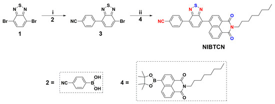
The synthetic route of NIBTCN is depicted in Scheme 1, and the detailed experimental procedures are offered in the Supporting Information. The intermediate compound 3 was acquired in 74% yield by reacting compound 1 with 2. Finally, the NIBTCN product was obtained in 40% yield by reacting compound 3 with 4 through the palladium-assisted reaction. These compounds were fully characterized through 1H NMR, 13C NMR, and elemental analysis (Figures S1–S4). It is worth mentioning that NIBTCN can retain its general property for more than one year in air. In addition, NIBTCN possesses an onset decomposition temperature over 330 °C (Figure S5), which suggests a good thermal stability.
Scheme 1.
Synthesis of the target NIBTCN material. (i) THF/H2O, Pd[P(Ph)3]4, yield of 74%; (ii) toluene/H2O, Pd2(dba)3, yield of 51%.
3.2. Optical and Electrochemical Properties
The optical and electrochemical measurements of NIBTCN were primarily conducted to study its optoelectronic behavior. As shown in Figure 1a, the UV/Vis absorption spectra of NIBTCN in CH2Cl2 solution and as thin-film state on silica glass were measured concurrently. In solution, NIBTCN exhibits three well-resolved absorptionpeaks. The most apparent low-energy absorption peak is located at 360 nm, which can be assigned to the intramolecular charge transfer (ICT) peak [26]. In film state, NIBTCN exhibits an obvious red-shift for the low-energy ICT absorbance peak. The ICT peak shifts to 370 nm, and the onset absorption wavelength (λonset) moves to 445 nm. Thus, the optical band-gap of NIBTCN is deduced to be ~2.79 eV. The emerged red-shift in film is correlated with the intermolecular arrangement in solid state [40].
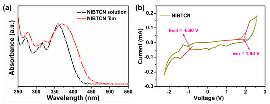
Figure 1.
(a) UV/Vis absorption spectra of NIBTCN in solution and as thin film on a quartz plate. (b) Cyclic voltammetry of NIBTCN accompanied with redox peaks.
Afterwards, cyclic voltammetry (CV) was utilized to inspect the electrochemical properties of NIBTCN.As shown in Figure 1b, NIBTCN exhibits an irreversible quasi-reversible oxidation and a quasi-reversible reduction peak during the cyclic potential scan. For calibration, the external ferrocene/ferrocenium (Fc+/Fc) redox was measured to be 0.39 eV vs. Ag/AgCl as a standard potential (EFc), where the absolute redox potential of Fc+/Fc is assumed to be −4.80 eV to vacuum [14]. Therefore, according to the equation EHOMO/LUMO = −e(4.80 − EFc + Eoxd/redonset) V, the HOMO and LUMO energy levels can be calculated to be −6.31 and −3.51 eV, with the onset oxidation and reduction potentials, respectively, located at +1.90 and −0.90 V. The energy band-gap of NIBTCN is about ~2.80 eV, which is in good agreement with the above UV/Vis optical value.
3.3. Film Morphology and Nanostructural Order
Generally speaking, organic electronic device performance significantly depends on the solid-state morphology and molecular arrangement of the related organic materials. To explore these properties, atomic force microscope (AFM) and X-ray diffraction (XRD) analysis were jointly conducted. As shown in Figure 2a, the AFM image shows that NIBTCN molecules appear a continuous nano-nodule-like texture in film with a rough width of 100–200 nm, and the surface roughness is about 0.77 nm. This smooth surface can favor to reduce the contact resistance among the interfaces, and hence warrant an effective interfacial charge transport channel. More intriguingly, the 3D-AFM image of NIBTCN film tends to exhibit multi-hills-like structures with preferential bottom-up orientations (Figure 2b,c). Note that the memory devices usually possess a vertical MIM structure: this prior morphology can promote charge transporting pathways along the vertical direction, which is beneficial for enhancing the device performance.
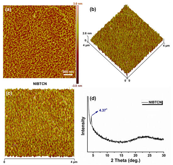
Figure 2.
(a) AFM image of NIBTCN film. (b,c) 3D-AFM images of NIBTCN film: (b) an angle view; (c) a top view. (d) XRD pattern of NIBTCN film.
XRD measurement was further performed to investigate the molecular arrangement order of NIBTCN in film (Figure 2d). XRD of NIBTCN shows a primary diffraction peak at 2θ = 4.37°, which is in accord with a d-spacing of 20.20 Å. This peak at small angle manifests that a well-ordered lamellar spacing structure generates in solid state [41]. The above film morphological and nanostructural characterizations encourage us to apply the prepared NIBTCN material for memory electronic devices.
3.4. Film Morphology and Nanostructural Order
For the fabrication of the resistive memory device, we deposited the NIBTCN molecules onto the ITO-coated silicate glass substrate, followed by the deposition of aluminum (Al) as top electrode through thermal evaporation technique. A schematic device structure is shown in Figure 3a and the corresponding cross-sectional scanning electron microscope (SEM) image is shown in Figure S6. Herein, we reported the measurements to explore the memory switching characteristics of our device. As shown in Figure 3b, a voltage sweep from 0 to −5.0 V is applied to the two terminal electrodes. The current response exhibits two distinct increases at −1.90 and −3.85 V, which reveals two resistive switching states with current ratios of 105.2/103.2/1 (Sweep 1). This process corresponds to the SET process [42], and the three states correspond to high-resistance state (HRS) intermediate-resistance state (IRS) and low-resistance state (LRS). Another cell was measured to examine the stability of IRS (Figure S7), which reveals that IRS can retain stable after the HRS-to-IRS transition. Once the device finishes the SET process, the LRS can also be well maintained, even under zero voltage bias, negative and positive voltage scans (Sweep 2 and 3). Such representative current–voltage (I–V) sweeps indicate nonvolatile irreversible ternary resistive memory behavior. In addition, the stability of the memory device has been studied through retention time test under a constant stress of −0.1 V. No obvious change of the device at IRS, IRS and LRS is detected for longer than 2 × 10³ s (Figure S8), which shows that the device is endurable under constant voltage stress and read pulses.
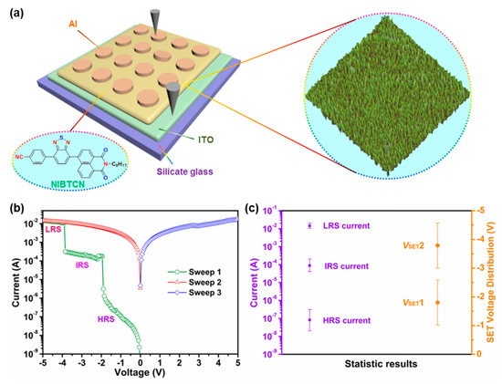
Figure 3.
(a) The schematic illustration of the metal-insulator-metal (MIM) type NIBTCN-based device, including silicate glass substrate, ITO, NIBTCN layer, and top Al electrode. (b) I–V characteristics of NIBTCN-based device. (c) The statistical data for the three current states (high-resistance state (HRS), intermediate-resistance state (IRS), low-resistance state (LRS)) and two threshold voltages (VSET1 and VSET2) of NIBTCN-based device depicted by error bars.
Moreover, to investigate the reproducibility of the resistive memory performance, we tested thirty independent units of the device for comparison. The memory device yield (i.e., the percentage of outputting resistive switching) is beyond 60%, which manifests acceptable reproducible performance. In addition, as the statistical data suggested, the three current states and two threshold voltages are well segregated (Figure 3c). The HRS current locates between 2.0 × 10⁻⁸ A and 3.0 × 10⁻⁷ A, while the IRS current locates between 4.0 × 10⁻⁵A and 2.0 × 10⁻⁴A, and the LRS current locates between 1.0 × 10⁻² A and 2.0 × 10⁻² A. For the threshold voltages, the first threshold voltage (VSET1) primarily ranges from−1.0 V to −2.4 V (probability of 80%) while the second threshold voltage (VSET2) primarily ranges from−3.4 V to−4.6 V (probability of 86%). The well-segregated distributions of currents and threshold voltages also reveal the satisfactory device reproducibility.
3.5. Proposed Resistive Memory Mechanism
To understand the ternary mechanism of D–A type NIBTCN, the molecular simulation through density functional theory (DFT) was performed through Gaussian 03 program at the B3LYP/6-31G basis. The molecular frontier orbitals of HOMO, LUMO, LUMO+1, and LUMO+2 are shown in Figure 4a. The electrons of HOMO are well-delocalized across the molecular skeleton. When undergoing HOMO to LUMO transition, the electrons mainly transfer to the electron-accepting BT/cyano side. At LUMO+1 level, the electrons tend to locate at the electron-accepting NI side. When further reaching LUMO+2 level, the electrons transfer to the electron-accepting BT/cyano side again. These intramolecular electron motions indicate that multiple charge transfer processes occur at the excited state, which can hence trigger multilevel resistance changes under the external electrical pulse. In addition, Figure 4b shows the energetic comparisons between molecular orbitals and electrodes. The electron injection energy barrier (Al/LUMO) is about 0.79 eV, which is smaller than the hole injection energy barrier (ITO/HOMO, 1.51 eV). This implies that the electron injection process is more energetically favorable during device operation [43].
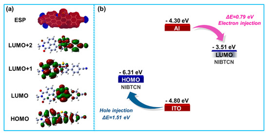
Figure 4.
(a) DFT simulated molecular electrostatic potential (ESP), HOMO, LUMO, LUMO+1, and LUMO+2 of NIBTCN. (b) The energy levels of HOMO/LUMO and the work functions of ITO/Al electrodes.
The calculation of molecular electrostatic potential (ESP) was subsequently conducted to study the influence of electron donors and acceptors among the molecular backbone. As shown in Figure 4a, a positive ESP (in red) area presents across the molecular skeleton of NIBTCN, leading to a fluent pathway for charge mobility. Nevertheless, several negative (blue) ESP areas appear at the middle and two sides of the molecular backbone, which are in accord with the locations of the electron acceptors, i.e., the BT, NI, and cyano groups. These negative ESP regions block the continuity of charge transport channel, which function as charge traps and thus induce multiple charge transfer processes to surmount these negative obstacles, causing charge retention and memory effects [42,44]. The above ESP calculations further verify the origin of the multiple charge transfer processes, which are responsible for the observed multilevel resistive switching behavior.
4. Discussion
In summary, the D–A type NIBTCN material was prepared and further utilized to fabricate an Al/NIBTCN/ITO memory device on ITO-coated glass through the thermal evaporation technique. The I–V curves of the as-prepared device exhibit an excellent resistive memory behavior with low threshold voltage, distinguishable resistive current ratios, good endurance, and favorable reproducibility. More importantly, the I–V curves show a ternary resistive switching behavior, which is promising for implementing higher data storage capacity. The formation of multiple charge transfer processes induced by different electron acceptors is proposed to explain the origin of the multistate resistive switching behavior. This work holds appealing promise to exhibit an application for future UHDDS memory logics and IoTs.
Supplementary Materials
The following are available online at https://www.mdpi.com/2079-6412/11/3/318/s1: Figure S1: 1H NMR spectrum of compound 3 in CDCl3; Figure S2: 1H NMR spectrum of compound 4 in CDCl3; Figure S3: 1H NMR spectrum of NIBTCN in CDCl3; Figure S4: 13C NMR spectrum of NIBTCN in CDCl3; Figure S5: TGA curve of NIBTCN at a heating rate of 10 °C min−1 under a nitrogen atmosphere; Figure S6:The cross-sectional SEM image of ITO/NIBTCN/Al device; Figure S7: I–V sweep curves of IRS for the ITO/NIBTCN/Al device; Figure S8: Retention stability of ITO/NIBTCN/Al device at HRS, IRS and LRS; Table S1: Detailed sweep profile and parameters of the device testing; Table S2: Optical and electrochemical properties of NIBTCN.
Author Contributions
Y.L., C.Z. and Z.S. contributed equally to this work. Investigation, Y.L. and C.Z.; methodology, Z.S. and J.L.; software, Q.Q. and S.L.; formal analysis, Y.Z. and X.Z.; visualization, X.W.; resources, J.Z. and Q.Z.; data curation, R.Z. and Y.J.; writing—original draft preparation, Y.L. and C.Z.; writing—review and editing, Y.L.; supervision, Y.L. and C.M.; funding acquisition, Y.L., J.Z. and Q.Z. All authors have read and agreed to the published version of the manuscript.
Funding
Y.L. thanks financial support from the National Natural Science Foundation of China (Grants No. 22008164), the Natural Science Foundation of Jiangsu Province (Grants No. BK20190939), and the Natural Science Foundation of the Jiangsu Higher Education Institutions of China (Grants No. 19KJB150018). This work is also supported by the Natural Science Foundation of China (11704272, 11804244, 21808149 and 62004136), the NSF of Jiangsu Province (BK20180965), the NSF of Jiangsu Higher Education Institutions (18KJA470004),Six Talent Peaks Project of Jiangsu Province, China (XCL-078), 2019 Undergraduate Innovation and Entrepreneurship Training Program of Jiangsu Province (201910332067Y), the Jiangsu Key Disciplines of the Thirteenth Five-Year Plan (20168765), and the Suzhou Key Laboratory for Low Dimensional Optoelectronic Materials and Devices(SZS201611).
Institutional Review Board Statement
Not applicable.
Informed Consent Statement
Not applicable.
Data Availability Statement
Data is contained within the article or supplementary materials.
Conflicts of Interest
The authors declare no conflict of interest.
References
- Wang, Y.; Sun, L.; Wang, C.; Yang, F.; Ren, X.; Zhang, X.; Dong, H.; Hu, W. Organic crystalline materials in flexible electronics. Chem. Soc. Rev. 2019, 48, 1492–1530. [Google Scholar] [CrossRef]
- Li, Y.; Qian, Q.; Zhu, X.; Li, Y.; Zhang, M.; Li, J.; Ma, C.; Li, H.; Lu, J.; Zhang, Q. Recent advances in organic-based materials for resistive memory applications. InfoMat 2020, 2, 995–1033. [Google Scholar] [CrossRef]
- Li, J.; Zhang, Q. Linearly Fused Azaacenes: Novel approaches and new applications beyond field-effect transistors (FETs). ACS Appl. Mater. Interfaces 2015, 7, 28049–28062. [Google Scholar] [CrossRef]
- Goswami, S.; Matula, A.-J.; Rath, S.-P.; Hedstrom, S.; Saha, S.; Annamalai, M.; Sengupta, D.; Patra, A.; Ghosh, S.; Jani, H.; et al. Robust resistive memory devices using solution-processable metal-coordinated azo aromatics. Nat. Mater. 2017, 16, 1216–1224. [Google Scholar] [CrossRef]
- Zhang, J.; Liu, G.; Zhou, Y.; Long, G.; Gu, P.; Zhang, Q. Solvent accommodation: Functionalities can be tailored through co-crystallization based on 1:1 coronene-F4TCNQ charge-transfer complex. ACS Appl. Mater. Interfaces 2017, 9, 1183–1188. [Google Scholar] [CrossRef]
- Ren, Y.; Chang, C.-L.; Ting, L.-Y.; Zhou, L.; Mao, J.-Y.; Zhang, S.-R.; Chou, H.-H.; Yang, J.-Q.; Zhou, Y.; Han, S.-T. Flexible pyrene/phenanthro [9, 10-d]imidazole-based memristive devices for mimicking synaptic plasticity. Adv. Intell. Syst. 2019, 1, 1900008. [Google Scholar] [CrossRef]
- Peng, C.; Ning, G.-H.; Su, J.; Zhong, G.; Tang, W.; Tian, B.; Su, C.; Yu, D.; Zu, L.; Yang, J.; et al. Reversible multi-electron redox chemistry of π-conjugated N-containing heteroaromatic molecule-based organic cathodes. Nat. Energy 2017, 2, 17074. [Google Scholar] [CrossRef]
- Leydecker, T.; Herder, M.; Pavlica, E.; Bratina, G.; Hecht, S.; Orgiu, E.; Samorì, P. Flexible non-volatile optical memory thin-film transistor device with over 256 distinct levels based on an organic bicomponent blend. Nat. Nanotechnol. 2016, 11, 769–775. [Google Scholar] [CrossRef] [PubMed]
- Ju, S.-E.; Yoon, C.-G.; Kim, J. Hybrid electroluminescence devices with solution-processed mixed emitting layers of red quantum dots and blue small molecules. Coatings 2020, 10, 645. [Google Scholar] [CrossRef]
- Shin, D.; Choi, S.-H. Recent studies of semitransparent solar cells. Coatings 2018, 8, 329. [Google Scholar] [CrossRef]
- Liu, J.; Yang, F.; Cao, L.; Li, B.; Yuan, K.; Lei, S.; Hu, W. A robust nonvolatile resistive memory device based on a freestanding ultrathin 2D imine polymer film. Adv. Mater. 2019, 31, 1902264. [Google Scholar] [CrossRef] [PubMed]
- Li, Y.; Zhu, X.; Li, Y.; Zhang, M.; Ma, C.; Li, H.; Lu, J.; Zhang, Q. Highly robust organometallic small-molecule-based nonvolatile resistive memory controlled by a redox-gated switching mechanism. ACS Appl. Mater. Interfaces 2019, 11, 40332–40338. [Google Scholar] [CrossRef]
- Keene, S.-T.; Melianas, A.; van de Burgt, Y.; Salleo, A. Mechanisms for enhanced state retention and stability in redox-gated organic neuromorphic devices. Adv. Electron. Mater. 2019, 5, 1800686. [Google Scholar] [CrossRef]
- Zhao, K.; Yu, F.; Liu, W.; Huang, Y.; Said, A.-A.; Li, Y.; Zhang, Q. Unexpected synthesis, properties, and nonvolatile memory device application of imidazole-fused azaacenes. J. Org. Chem. 2020, 85, 101–107. [Google Scholar] [CrossRef] [PubMed]
- Kim, J.; Ohtsu, H.; Den, T.; Deekamwong, K.; Muneta, I.; Kawano, M. Control of anisotropy of a redox-active molecule-based film leads to non-volatile resistive switching memory. Chem. Sci. 2019, 10, 10888–10893. [Google Scholar] [CrossRef]
- Li, Y.; Zhu, X.; Qian, Q.; Ma, C.; Zhang, M.; Shi, Z.; Kuai, J.; Zhang, Y.; Yan, Z.; Zhang, Q. Nonvolatile flexible memory based on a planar zigzag-type nitrogen-doped picene. Adv. Intell. Syst. 2020, 2, 2000155. [Google Scholar] [CrossRef]
- Zhao, J.; Li, H.; Li, H.; Zhao, Q.; Ling, H.; Li, J.; Lin, J.; Xie, L.; Lin, Z.; Yi, M.; et al. Synthesis, characterization and charge storage properties of π-biindolo[2,3-b]quinoxaline for solution-processing organic transistor memory. Dye. Pigment. 2019, 167, 255–261. [Google Scholar] [CrossRef]
- Li, Y.; Zhang, C.; Li, Z.; Gu, P.; Wang, Z.; Li, H.; Lu, J.; Zhang, Q. Controlled deposition of large-area and highly-ordered thin films: Effect of dip-coating-induced morphological evolution on resistive memory performance. J. Mater. Chem. C 2019, 7, 3512–3521. [Google Scholar] [CrossRef]
- Xu, J.; Zhao, X.; Wang, Z.; Xu, H.; Hu, J.; Ma, J.; Liu, Y. Biodegradable natural pectin-based flexible multilevel resistive switching memory for transient electronics. Small 2019, 15, 1803970. [Google Scholar] [CrossRef]
- Zhang, B.; Fan, F.; Xue, W.; Liu, G.; Fu, Y.; Zhuang, X.; Xu, X.H.; Gu, J.; Li, R.-W.; Chen, Y. Redox gated polymer memristive processing memory unit. Nat. Commun. 2019, 10, 736. [Google Scholar] [CrossRef]
- Li, Y.; Wang, Z.; Zhang, C.; Gu, P.; Chen, W.; Li, H.; Lu, J.; Zhang, Q. Thiadizoloquinoxaline-based N-heteroacenes as active elements for high-density data-storage devic. ACS Appl. Mater. Interfaces 2018, 10, 15971–15979. [Google Scholar] [CrossRef]
- Chan, H.; Wong, H.-L.; Ng, M.; Poon, C.-T.; Yam, V.-W. Switching of resistive memory behavior from binary to ternary logic via alteration of substituent positioning on the subphthalocyanine core. J. Am. Chem. Soc. 2017, 139, 7256–7263. [Google Scholar] [CrossRef]
- Yi, X.; Yu, Z.; Niu, X.; Shang, J.; Mao, G.; Yin, T.; Yang, H.; Xue, W.; Dhanapal, P.; Qu, S.; et al. Intrinsically stretchable resistive switching memory enabled by combining a liquid metal-based soft electrode and a metal-organic framework insulator. Adv. Electron. Mater. 2019, 5, 1800655. [Google Scholar] [CrossRef]
- Tang, J.-H.; Sun, T.-G.; Shao, J.-Y.; Gong, Z.-L.; Zhong, Y.-W. Resistive memory devices based on a triphenylamine-decorated non-precious cobalt(ii) bis-terpyridine complex. Chem. Commun. 2017, 53, 11925–11928. [Google Scholar] [CrossRef]
- Hu, B.; Wang, C.; Wang, J.; Gao, J.; Wang, K.; Wu, J.; Zhang, G.; Cheng, W.; Venkateswarlu, B.; Wang, M.; et al. Inorganic–organic hybrid polymer with multiple redox for high-density data storage. Chem. Sci. 2014, 5, 3404–3408. [Google Scholar] [CrossRef]
- Zhang, C.; Li, H.; Lin, S.; Su, Y.; Zhang, Q.; Li, Y.; Wang, K.; Lu, J. Fabrication of one-dimensional organic nanofiber networks via electrophoretic deposition for a nonvolatile memory device. ACS Appl. Mater. Interfaces 2020, 12, 57254–57263. [Google Scholar] [CrossRef] [PubMed]
- Wang, C.; Gu, P.; Hu, B.; Zhang, Q. Recent progress in organic resistance memory with small molecules and inorganic–organic hybrid polymers as active elements. J. Mater. Chem. C 2015, 3, 10055–10065. [Google Scholar] [CrossRef]
- Hu, B.; Zhu, X.; Chen, X.; Pan, L.; Peng, S.; Wu, Y.; Shang, J.; Liu, G.; Yan, Q.; Li, R.-W. A multilevel memory based on proton-doped polyazomethine with an excellent uniformity in resistive switching. J. Am. Chem. Soc. 2012, 134, 17408–17411. [Google Scholar] [CrossRef]
- Wu, Z.-H.; Sun, W.-J.; Tian, H.-H.; Yu, Z.-F.; Guo, R.-X.; Shao, X.; Zhang, H.-L. 9,10-Imide-pyrene-fused pyrazaacenes (IPPA) as n-type doping materials for high-performance nonvolatile organic field effect transistor memory devices. Adv. Electron. Mater. 2019, 5, 1800598. [Google Scholar] [CrossRef]
- Zhang, C.; Li, Y.; Zhou, Y.; Zhang, Q.; Li, H.; Lu, J. Deriving highly oriented organic nanofibers and ternary memory performance via salification-induced effects. Chem. Commun. 2018, 54, 10610–10613. [Google Scholar] [CrossRef]
- Gao, S.; Yi, X.; Shang, J.; Liu, G.; Li, R.-W. Organic and hybrid resistive switching materials and devices. Chem. Soc. Rev. 2019, 48, 1531–1565. [Google Scholar] [CrossRef]
- Zhou, L.; Mao, J.; Ren, Y.; Han, S.-T.; Roy, V.-A.-L.; Zhou, Y. Recent advances of flexible data storage devices based on organic nanoscaled materials. Small 2018, 14, 1703126. [Google Scholar] [CrossRef]
- Zheng, Y.Q.; Lei, T.; Dou, J.-H.; Xia, X.; Wang, J.-Y.; Liu, C.-J.; Pei, J. Strong electron-deficient polymers lead to high electron mobility in air and their morphology-dependent transport behaviors. Adv. Mater. 2016, 28, 7213–7219. [Google Scholar] [CrossRef]
- Yi, Z.; Wang, S.; Liu, Y. Design of high-mobility diketopyrrolopyrrole-based π-conjugated copolymers for organic thin-film transistors. Adv. Mater. 2015, 27, 3589–3606. [Google Scholar] [CrossRef]
- Zhang, Q.; He, J.; Zhuang, H.; Li, H.; Li, N.; Xu, Q.; Chen, D.; Lu, J. Rational design of small molecules to implement organic quaternary memory devices. Adv. Funct. Mater. 2016, 26, 146–154. [Google Scholar] [CrossRef]
- Zhang, J.; Gu, P.; Long, G.; Ganguly, R.; Li, Y.; Aratani, N.; Yamada, H.; Zhang, Q. Switching charge-transfer characteristics from p-type to n-type through molecular “doping” (co-crystallization). Chem. Sci. 2016, 7, 3851–3856. [Google Scholar] [CrossRef] [PubMed]
- Nketia-Yawson, B.; Lee, H.-S.; Seo, D.; Yoon, Y.; Park, W.-T.; Kwak, K.; Son, H.-J.; Kim, B.; Noh, Y.-Y. A highly planar fluorinated benzothiadiazole-based conjugated polymer for high-performance organic thin-film transistors. Adv. Mater. 2015, 27, 3045–3052. [Google Scholar] [CrossRef] [PubMed]
- Jung, J.-W.; Jo, W.-H. Low-bandgap small molecules as non-fullerene electron acceptors composed of benzothiadiazole and diketopyrrolopyrrole for all organic solar cells. Chem. Mater. 2015, 27, 6038–6043. [Google Scholar] [CrossRef]
- Zhao, Z.; Yin, Z.; Chen, H.; Zheng, L.; Zhu, C.; Zhang, L.; Tan, S.; Wang, H.; Guo, Y.; Tang, Q.; et al. High-performance, air-stable field-effect transistors based on heteroatom-substituted naphthalenediimide-benzothiadiazole copolymers exhibiting ultrahigh electron mobility up to 8.5 cm2 V−1 s−1. Adv. Mater. 2017, 29, 1602410. [Google Scholar] [CrossRef]
- Li, Y.; Li, H.; Chen, H.-F.; Wan, Y.; Li, N.-J.; Xu, Q.-F.; He, J.-H.; Chen, D.-Y.; Wang, L.-H.; Lu, J.-M. Controlling crystallite orientation of diketopyrrolopyrrole-based small molecules in thin films for highly reproducible multilevel memory device: Role of furan substitution. Adv. Funct. Mater. 2015, 25, 4246–4254. [Google Scholar] [CrossRef]
- Wang, J.-T.; Takashima, S.; Wu, H.-C.; Chiu, Y.-C.; Chen, Y.; Isono, T.; Kakuchi, T.; Satoh, T.; Chen, W.-C. Donor-acceptor poly(3-hexylthiophene)-block-pendent poly(isoindigo) with dual roles of charge transporting and storage layer for high-performance transistor-type memory applications. Adv. Funct. Mater. 2016, 26, 2695–2705. [Google Scholar] [CrossRef]
- Zhang, C.; Li, H.; Su, Y.; Zhang, Q.; Li, Y.; Lu, J. Controllable and versatile electrophoretic deposition technology for monolithic organic memory devices. ACS Appl. Mater. Interfaces 2020, 12, 15482–15490. [Google Scholar] [CrossRef] [PubMed]
- Poon, C.-T.; Wu, D.; Yam, V.-W. Boron(III)-containing donor-acceptor compound with goldlike reflective behavior for organic resistive memory devices. Angew. Chem. Int. Ed. 2016, 55, 3647–3651. [Google Scholar] [CrossRef]
- Bao, Q.; Li, H.; Li, Y.; He, J.; Xu, Q.; Li, N.; Chen, D.; Wang, L.; Lu, J. Comparison of two strategies to improve organic ternary memory performance: 3-Hexylthiophene linkage and fluorine substitution. Dye. Pigment. 2016, 130, 306–313. [Google Scholar] [CrossRef]
Publisher’s Note: MDPI stays neutral with regard to jurisdictional claims in published maps and institutional affiliations. |
© 2021 by the authors. Licensee MDPI, Basel, Switzerland. This article is an open access article distributed under the terms and conditions of the Creative Commons Attribution (CC BY) license (http://creativecommons.org/licenses/by/4.0/).