Article

Nanoindentation Hardness and Practical Scratch Resistance in Mechanically Tunable Anti-Reflection Coatings

1
Corning Incorporated, Corning, NY 14831, USA
2
Corning Incorporated, Asan-si, Chungcheongnam-do 336-725, Korea
*
Author to whom correspondence should be addressed.
Coatings 2021, 11(2), 213; https://doi.org/10.3390/coatings11020213
Submission received: 31 December 2020 / Revised: 5 February 2021 / Accepted: 8 February 2021 / Published: 12 February 2021
(This article belongs to the Special Issue Mechanical Properties of Advanced Multifunctional Coatings)

Abstract

:
This work presents fundamental understanding of the correlation between nanoindentation hardness and practical scratch resistance for mechanically tunable anti-reflective (AR) hardcoatings. These coatings exhibit a unique design freedom, allowing quasi-continuous variation in the thickness of a central hardcoat layer in the multilayer design, with minimal impact on anti-reflective optical performance. This allows detailed study of anti-reflection coating durability based on variations in hardness vs. depth profiles, without the durability results being confounded by variations in optics. Finite element modeling is shown to be a useful tool for the design and analysis of hardness vs. depth profiles in these multilayer films. Using samples fabricated by reactive sputtering, nanoindentation hardness depth profiles were correlated with practical scratch resistance using three different scratch and abrasion test methods, simulating real world scratch events. Scratch depths from these experiments are shown to correlate to scratches observed in the field from consumer electronics devices with chemically strengthened glass covers. For high practical scratch resistance, coating designs with hardness >15 GPa maintained over depths of 200–800 nm were found to be particularly excellent, which is a substantially greater depth of high hardness than can be achieved using previously common AR coating designs.

1. Introduction

Optical interference coatings utilize the physics of thin-film interference [1,2,3,4] to create unique optical properties that cannot be achieved using typical bulk materials. These coatings have been studied and applied for a broad variety of uses, including low reflection optics [4,5], high reflection mirrors [6,7,8], solar energy management [9], telecommunications [10], infrared (IR) sensors [11,12] and more. Despite this broad design flexibility and utility, optical interference coatings, especially anti-reflective (AR) interference coatings, have historically suffered from relatively low scratch or damage resistance, especially when compared to modern chemically strengthened glasses such as Corning® Gorilla® Glass. This relatively low durability remains true even for coatings using thin layers of materials which can have high hardness such as silicon nitride [13,14], because the design of these coatings relies on layers that are too thin (~0.1 micron or less) to protect the coating or the underlying substrate against common scratches in these types of applications. AR coatings are especially prone to high scratch visibility, due to high optical contrast (change in reflectivity) between the scratched and unscratched regions that readily occurs for scratches as shallow as ~50 nm.
In recent work, a new opto-mechanical design approach has been described enabling the production of anti-reflection coatings with very high hardness and scratch resistance [15,16]. Two key elements of this new coating design approach include: (1) A unique “modular” optical design approach which de-couples the optical performance of the coating from the thickness of a central high-hardness layer (the “hardcoat” layer or H-layer) in the multilayer design, and (2) selection of overall hardness vs. depth profiles of the coating to enable very high scratch resistance in aggressive real-world scratch events, such as those encountered in field trials of consumer electronics devices subject to daily handling. In this paper, the fundamental hardness and optical properties enabled by this tunable approach are further illuminated. Analysis of real-world field scratches from consumer electronics devices is used to establish a typical range of scratch depths in this field of use, which guides coating design choices for this application. Starting with a single-layer analysis, measured nanoindentation hardness vs. depth profiles are explained, considering a combination of substrate and coating effects. Extending this analysis to multilayer anti-reflection coatings, both modeling and experiments are used to show how this unique design approach enables the production of anti-reflection coatings with tunable hardness vs. depth profiles. Mechanical tuning through quasi-continuous thickness variation of the central hardcoat layer is shown to have minimal impact on the optical anti-reflection performance. This tunability allows for the ideal design to be selected from a broad range of options, depending on the level of hardness and scratch resistance that is desired for a particular end-use application. Finite element modeling is shown to be effective in predicting hardness vs. depth profiles in these multilayer anti-reflective hardcoatings. Finally, a high level of hardness maintained over extended depths is shown to correlate to scratch resistance in aggressive scratch testing designed to mimic severe real-world use conditions.

2. Materials and Methods

2.1. Coating Design and Fabrication

Anti-reflective, high-hardness coatings were designed using optical transfer matrix simulations [1], incorporating optical properties measured by spectroscopic ellipsometry for the experimentally fabricated coating materials. Coatings were made using reactive sputtering deposition processes [17,18,19,20]. These sputtering fabrication processes have been found to deliver desirable combinations of coating density, stress, hardness, optical absorption, layer thickness control, and deposition rates, enabling efficient manufacturing. Exemplary multilayer coatings are comprised of high hardness, high refractive index materials, such as SiNx, SiOxNy, AlOxNy, or SiAluOxNy, layered with a low-index material, such as SiO2. In this work, metallic aluminum or silicon sputtering targets were combined with non-reactive argon and reactive oxygen and nitrogen process gases in a sputtering chamber. For each coating material and sputtering process, a recipe development specific to each coating chamber geometry was required to achieve the desired targets of low optical extinction coefficient (k < 0.001 at 400 nm wavelength), high material hardness (>18 GPa for a single-material, 2-micron thick layer), and low or controlled film stress (0–400 MPa compressive). In order to achieve high hardness levels using SiNx, SiOxNy, AlOxNy, or SiAluOxNy materials, film compositions may include 0–20 atom% oxygen and 30–50 atom% nitrogen, with resulting refractive indices in the range of 1.9–2.1.
As an exemplary process, high hardness, high optical transparency SiOxNy film materials can be deposited by reactive magnetron sputtering from a silicon target [17,18]. Using a laboratory deposition chamber (ATC-2200 with A330-XP UHV magnetron sputtering source from AJA International (N. Scituate, MA, USA)) with 3″ sputtering targets, example process conditions for SiOxNy deposition on glass substrates included 400 W RF power to the Si target supplied at 13.56 MHz, 30 sccm Ar gas flow, 40 sccm N2 gas flow, 0.4 sccm O2 gas flow, 1.5 mTorr process pressure, and a deposition temperature of 100–200 °C. These process conditions led to SiOxNy film materials with a refractive index of ~1.9 and measured hardness of >17 GPa, with a corresponding composition of ~48 atom% Si, 10 atom% O, and 42 atom% N. Using a similar process with O2 gas flow set to zero, SiNx or SiOxNy materials with only trace amounts of oxygen were deposited with a refractive index >2.0 and measured hardness >20 GPa. For films in this range of hardness, typical elastic modulus values were in the range of 200–240 GPa, resulting in H/E ratios of ~0.1.
These high-index, high-hardness materials were layered with a low-index material, typically SiO2, to achieve the optical interference effects driving anti-reflection. It is necessary to have a low-index material component of the coating to achieve the desired interference effects, and materials with low refractive index typically have lower levels of hardness (due to the relationship of both hardness and refractive index to electron and bonding density in the materials). Lower-index, lower-hardness SiO2 films can be made using similar deposition processes as those described above for SiNx and SiOxNy, replacing N2 gas flow with O2 gas flow only. All coated samples, as well as the chemically strengthened glasses without hard coatings used for comparison, included a very thin (<10 nm) oleophobic fluorosilane layer on the top-most user-facing surface. These coatings are common on glasses in consumer electronics applications and tend to reduce the friction of the surface without having a significant effect on optics or hardness.
The opto-mechanical design strategy used to create high-hardness anti-reflective coatings [16] conceptually divides the coating into one or more optical interference layer regions, which perform the desired optical functions, and one or more hardcoat layer regions, which provide high levels of hardness at depths that are typical of real-world scratch events. In many cases the same material can be used for both the hardcoat region and the high-index component of the optical interference layer regions, while a softer low-index material is needed in the layered regions to create the desired optical interference effects. For anti-reflective coatings, multiple interference layer regions are employed for lower reflectance; the anti-reflective layers near the glass-to-hardcoat interface are also called “impedance matching” layers, to distinguish them from the AR layers adjacent to the user-facing, air-exposed surface. This combination of impedance-matching AR layers at the glass-to-hardcoat interface, together with the AR layers at the hardcoat-to-air interface, is what enables the uniquely tunable thickness (minimal optical change with thickness change) of the thick “hardcoat” layer.

2.2. Optical and Nanoindentation Measurements

Optical reflection and transmission spectroscopy were performed using an Agilent Cary 5000 UV-Vis-NIR spectrophotometer (Santa Clara, CA, USA) recording spectra with 2 nm wavelength step size and 4 nm resolution. The spectra were used to determine CIE L*a*b* color coordinates and perform reverse engineering of the designs. A Woollam M-2000 variable-angle spectroscopic ellipsometer, varying the input angle of the measurement from 45° to 80° and scanning the wavelength from 250 to 1680 nm, was used to analyze film thickness and refractive index. These measurements were used to determine single-layer film material dispersion and deposition rates for individual processes, as well as to reverse-engineer the refractive index and thickness for film stacks consisting of multiple layers.
Coating hardness was measured via nanoindentation using a Berkovich diamond tip on a KLA Instruments G200 Nano Indenter (Milpitas, CA, USA). Hardness was extracted using the widely accepted Oliver–Pharr approach [21,22], combined with a special technique known as the continuous stiffness measurement [23]. The continuous stiffness measurement technique superimposed a small (+/−1 nm) oscillatory signal at 52 Hz during the loading cycle, which enabled the hardness to be measured continuously as a function of indentation depth. The system can reach a maximum indentation depth of 500 µm (resolution of 0.2 nm) and a maximum load of 630 mN (resolution of 50 nN). A Berkovich indenter tip, made from a single crystal diamond, was used in this investigation. A constant indentation strain rate of 0.05 s−1 was maintained during the loading stage. The amplitude of harmonic oscillation was 1 nm. Nanoindentations at 10 different locations were conducted on each sample, with typical standard deviations of hardness in the range of 0.3–0.5 GPa.
Analyses were carried out to determine the mechanical properties (hardness and modulus) based on the contact mechanics analysis of nanoindentation load-depth relationships, which has been well established by Oliver and Pharr [21,22].
The indentation hardness (H) is obtained using
H = P m a x A c
where Pmax is the maximum nanoindentation load, Ac is the contact area corresponding to the contact depth (hc) at the maximum load.
The contact stiffness S = d P / d h is calculated from the slope of the initial unloading cure, and the reduced modulus is obtained by,
E r = 1 2 β π A c d P d h
where β is the indenter shape correction factor [21]. The reduced modulus Er is related to the specimen’s Young’s modulus by,
1/Er = (1 − νs2)/Es + (1 − νi2)/Ei
where Es and νs are the Young’s modulus and Poisson’s ratio of the specimen, respectively, while Ei and νi are the Young’s modulus and Poisson’s ratio of the diamond Berkovich indenter tip, respectively.
The contact depth hc is given by,
h c = h m a x ε P m a x S  
Oliver and Pharr found that experimental results on standard specimens that indicated ε = 0.75 best accounts for the material behavior [21]. The area function was calibrated on a reference sample of fused silica. The area function, which accounts for the non-ideal shape of a real indenter, was fitted into the following polynomial,
A c = 25.746 h c 2 + 1383.2 h c 6942.11 h c 1 / 2 + 6670.6 h c 1 / 4
where the contact depth hc has a unit of nm. Since the continuous stiffness measurement (CSM) method imposes a harmonic displacement (1 nm) during loading, the unloading stiffness can be obtained continuously, and thus, Young’s modulus and hardness as a function of nanoindentation depth can be obtained based on the Oliver–Pharr analysis shown above.

2.3. Scratch Resistance Tests

In order to establish correlations between hardness vs. depth profiles and practical scratch resistance, three different controlled scratch tests were employed. These scratch tests were chosen because they create scratches with similar morphology and depth to the most frequent scratches observed in field studies of chemically strengthened glass covers for consumer electronics devices. The first “nano-scratch” test involves controlled scratching with a diamond tip using a KLA G200 nano indenter with scratch option. Using a Berkovich diamond tip, a constant load scratch of 500 µm length is applied at 50 µm/s velocity. The resulting scratch depth is then measured using the Berkovich tip as a surface profilometer by applying an ultra-light load of 50 micro-Newtons. This method of depth profiling has been found to give values close to an atomic force microscope (AFM), in the depth ranges of interest. The diamond scratch test gives precise and repeatable results, however, most real-world scratch events do not involve an abrasive as hard as diamond, so other methods were also evaluated. A second test method evaluated was reciprocating abrasion with 400 grit Al2O3 sandpaper from Kovax (Tokyo, Japan), using a 700 g load applied over a ~1 cm × 1 cm contact area for 50 reciprocating cycles (40 cycles/min, 1.5 inch long stroke length). This test method is more properly categorized as abrasion or wear, due to the reciprocating cycles, which are not typically observed in real-world scratch events. However, this method was chosen because of its relevance to surface durability and its ability to create a semi-uniform area of multiple scratches which can be quantified using light scattering methods. Light scattering is particularly relevant to optical coatings such as anti-reflection coatings, and was quantified using a reflective scattered light measurement with specular component excluded (SCE) measurement using a Konica-Minolta CM700D with a 6 mm diameter aperture [24,25]. Finally, a garnet scratch test method was evaluated consisting of a single pass with 150 grit garnet sandpaper, with 1 kg applied load over a ~0.6 cm diameter contact area. This garnet scratch test is the closest to simulating real-world scratch events, due to the single-pass nature of the test and the intermediate hardness of garnet, which is moderately harder than common real-world abradants such as sand. The garnet scratch test yields relatively sparse and random scratches which are difficult to analyze using light scattering, so this test was quantified using an atomic force microscope (AFM) measurement of each scratch that was visible to the naked eye, in the center of the scratch path.

3. Results

3.1. Field Analysis of Real-World Scratch Events

To establish a baseline target of real-world scratch events, the consumer electronics industry was chosen as our application focus. Consumer touch-screen devices with chemically strengthened glass covers were subjected to typical daily usage handling by actual consumers in the field, and were then characterized for the type, depth, and severity of observed scratches. About 75% of the observed scratches were characterized as single-event, groove-like micro-ductile type scratches [26], while about 25% were associated with some level of cracking or chipping. Focusing on the most frequently observed micro-ductile scratches, the scratch depths of these were measured using atomic force microscopy (AFM). The measured distribution of scratch depths is shown in Figure 1. The majority of the measured micro-ductile scratch depths are in the 100–500 nm depth range. This suggests that coating or surface hardness in this depth range is of particular importance in preventing these types of frequent real-world scratch events.

3.2. Single-Layer Hardness Profiles vs. Scratch Depth

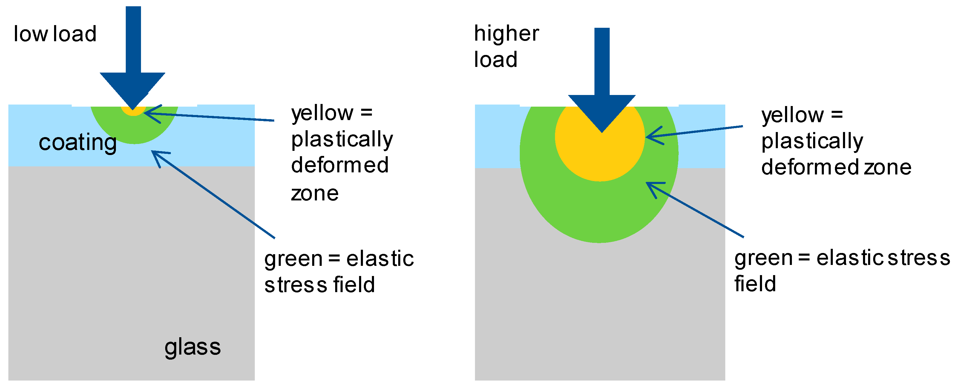
Informed by the scratch depths of interest from Figure 1, single-layer hardcoatings of varying thickness were studied for initial understanding of their effectiveness in suppressing scratches in this depth range. Considering the fundamentals of the nanoindentation hardness measurement, it is important to keep in mind how the indenter interacts with a coated material. As shown schematically in Figure 2, the region of permanent deformation (plastic zone) is associated with the hardness of the material. However, as shown in Figure 2, an elastic stress field extends well beyond this region of permanent deformation, meaning the indenter has an interaction field that can be considerably larger than the thickness of a thin film. As the indentation depth increases, the apparent hardness and modulus are influenced by stress field interactions with the substrate. The modulus is influenced by the substrate almost immediately, as the indenter begins to penetrate the sample surface since the region of elastic deformation extends far enough to interact with the substrate, even upon initial shallow indentation. The region of plastic deformation has a smaller extent than the region of elastic deformation. This has the result that substrate influence on hardness occurs at deeper indentation depths, since deeper penetration is needed to extend the region of plastic deformation that influences hardness to interact with the substrate. A transition where the hardness of the substrate begins to have an influence is typically observed when the indentation depth is ~30% of the coating thickness. Importantly, these volumetric interactions are related to the fundamental mechanics of contact damage, and can be expected to be similarly present in real-world scratching events. This means that the practical scratch resistance of a hardcoated surface may not only depend on the hardness of a thin film layer, but also on the hardness vs. depth profile and the interaction of multiple layers, up to—and potentially including—the substrate on which the coating is formed.
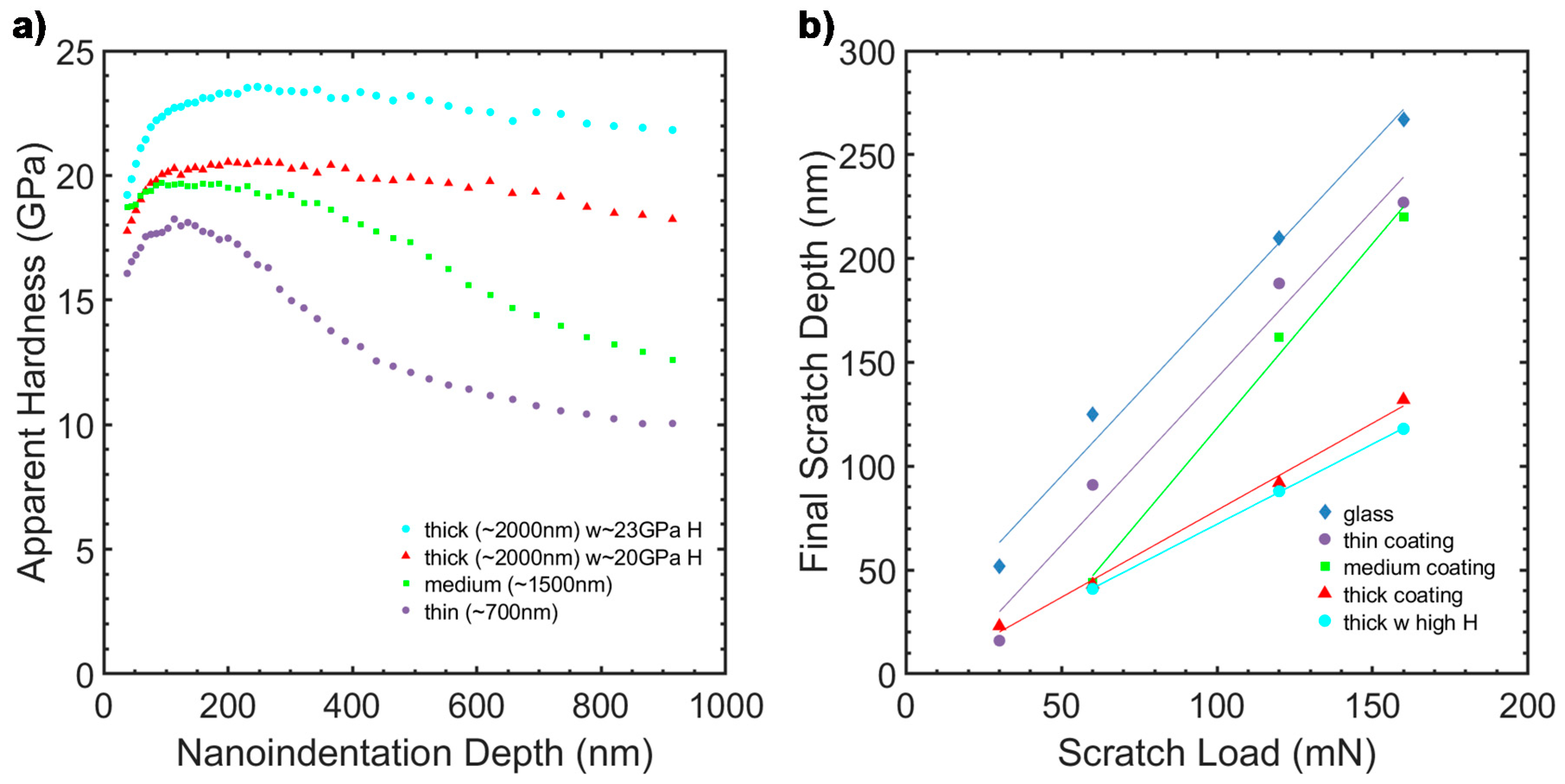
Figure 3a shows how these interactions impact the measured hardness vs. depth profiles for a series of single-layer SiOxNy films of varying thickness coated on aluminosilicate glass substrates. At shallow depths <~100 nm, the hardness response requires a certain minimum load to develop full plasticity during the indentation process, causing the hardness to show a generally increasing trend at these shallow depths. The hardness then reaches a “plateau” and begins to drop gradually as the substrate interaction effects take on a larger role at deeper indentation depths. In Figure 3, the thin (700 nm), medium (1500 nm), and thick (2000 nm w ~20 GPa H) films were all deposited using the same process conditions, but the measured apparent hardness profiles of these three films vary substantially due to their differing thickness. The 700 nm film has a lower peak hardness, which is largely due to the aforementioned effects which can suppress measured hardness at both shallow depths and deeper depths. It is likely that these effects prevent us from measuring the “true” film hardness of this 700 nm coating. For the 1500 nm and 2000 nm films, a plateau occurs at approximately the same hardness level near ~20 GPa. This suggests that ~20 GPa is near the “true” hardness of these films, and that this true hardness can only be measured when the film is sufficiently thick. For comparison, the hardness of typical chemically strengthened glass without coatings is approximately ~8 GPa. The final thick sample (2000 nm w ~23 GPa H) was deposited using tuned process conditions to further maximize hardness, such as slightly lowering deposition pressure, slightly increasing deposition plasma energy, and small reductions in oxygen/increased nitrogen levels. While these changes can have a negative impact on other properties such as optical absorption and film stress, these conditions were tested here to compare the effects of thickness vs. hardness in scratch test measurements.
Figure 3b shows the results of Berkovich diamond nano-scratch testing on the same series of SiOxNy films. The nano-scratch depths cover a range up to 270 nm deep, which falls within the range that has been observed for real world micro-ductile scratches in consumer electronics devices, as described above. Interestingly, the 2000 nm thick coatings were the only ones that maintained their ability to significantly reduce scratch depth over this entire range of scratch severity. These thicker coatings were found to reduce the scratch depths by >50% compared to uncoated chemically strengthened aluminosilicate glass. A modest increase in coating hardness from 20 GPa to 23 GPa for the 2000 nm thick films resulted in only a marginal benefit, suggesting that coating thickness (hardness vs. depth profile) had a much stronger influence on scratch resistance over the ranges tested. These results suggest that most common AR coatings, which typically have total coating thicknesses of about 300–500 nm (including both high- and low-index materials) should not be expected to significantly reduce scratch severity in this range of depth and force when compared to chemically strengthened glass. This is true even if those common AR coatings incorporate layers of high-hardness materials.

3.3. Mechanically Tunable Multilayer Anti-Reflective Hardcoatings (AR-HCs)

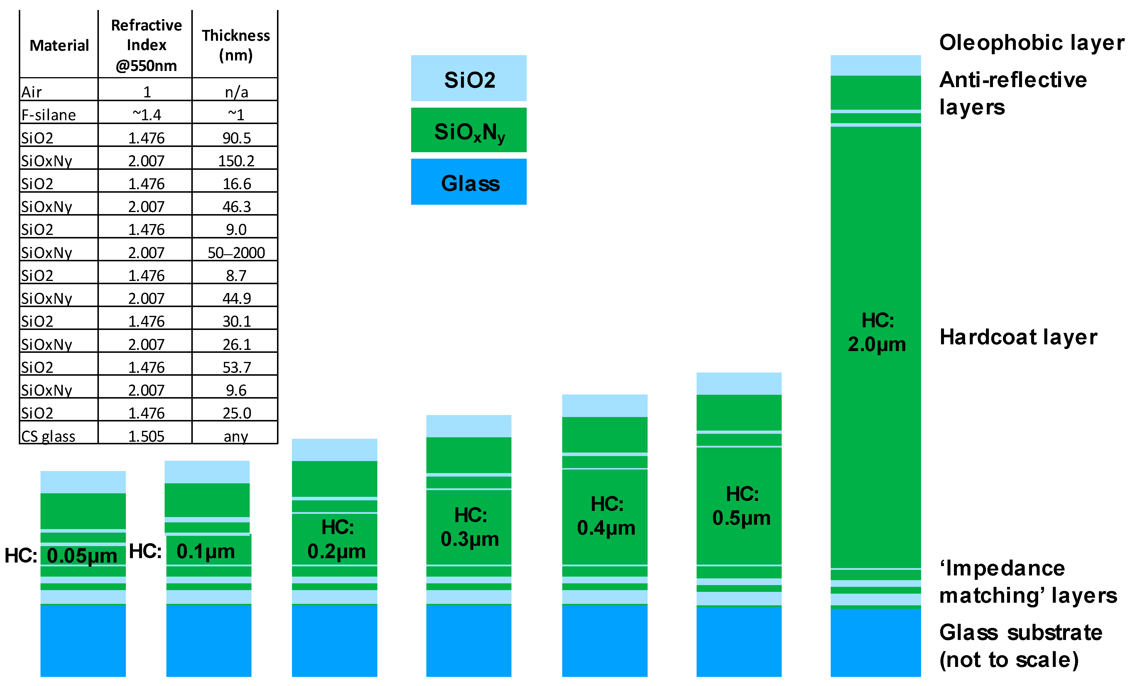
To extend the analysis above to multilayer anti-reflection coatings, a series of anti-reflective hardcoatings (AR-HCs) were fabricated with nearly identical optics, but varying hardness vs. depth profiles. The fabricated coatings are depicted schematically in Figure 4, with detailed layer thicknesses given in the inset table. These coatings use the modular opto-mechanical design approach of [16]. An anti-reflective series of layers, also called impedance-matching layers, between the glass substrate and a central hardcoating layer substantially de-couples the optical performance of the multilayer stack from the thickness of this central layer, which is a unique feature not present in previously common anti-reflection coating designs. This allows the mechanical tuning of these anti-reflection coatings through varying the thickness of this central hardcoating layer, enabling the creation of varying hardness vs. depth profiles while maintaining a nearly identical optical performance. Upon evaluation of the hardness and scratch resistance of these anti-reflection coatings, optimal designs can be chosen that have the required scratch resistance for specific applications.
Figure 5 illustrates the measured first-surface reflectance of the series of AR-HCs compared to an uncoated chemically strengthened (CS) glass control sample. Of note is the strikingly similar reflectance vs. wavelength performance shown for all coatings, despite the variation in central hardcoating layer thickness. This is a unique feature enabled by the modular anti-reflective hardcoating design approach, and enables visual or optical comparisons of damage resistance that are not confounded with changes in AR coating optics.
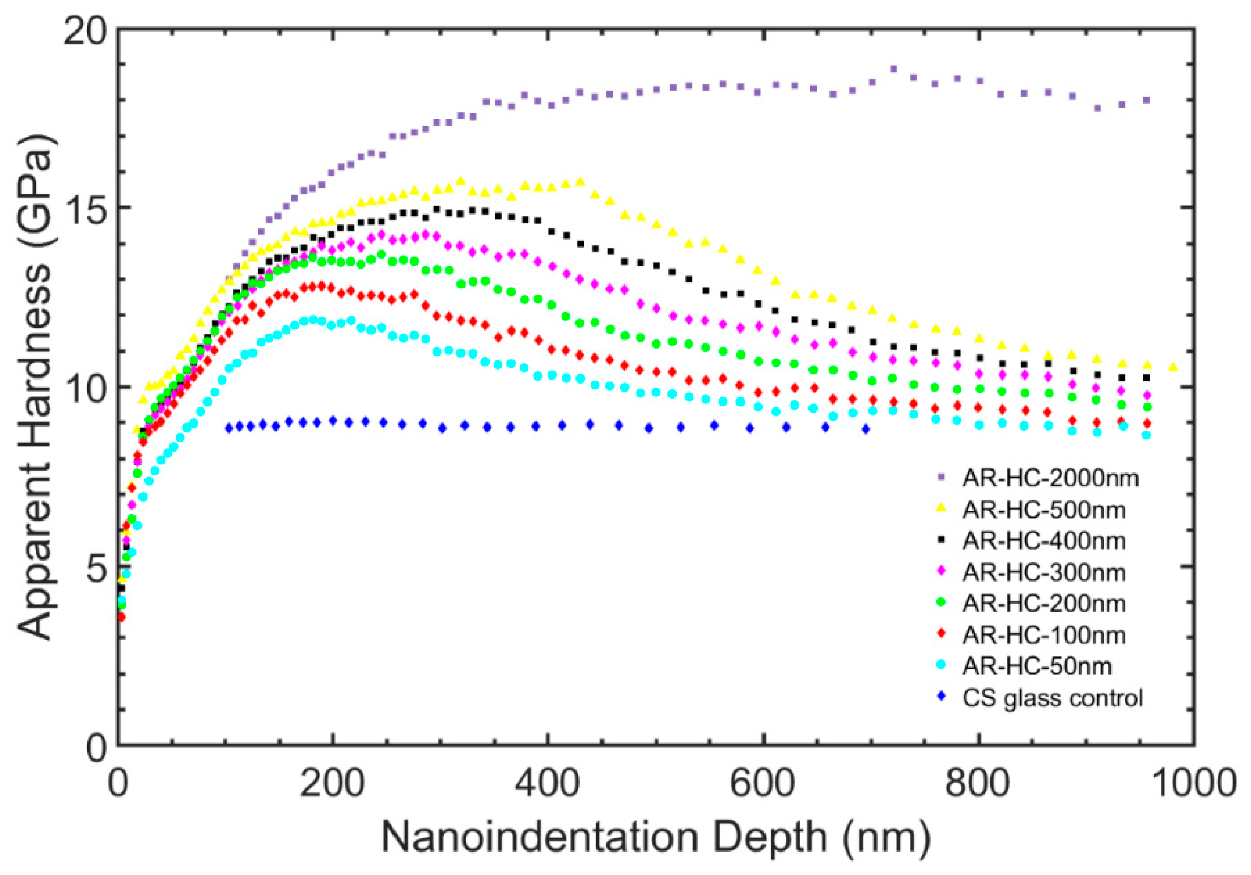
Figure 6 shows the measured nanoindentation depth vs. hardness profiles for the series of AR-HCs fabricated for this study, compared to uncoated chemically strengthened (CS) glass. As was seen for the single-layer hardcoatings, the hardness vs. depth profiles of the AR-HCs are strongly dependent on the thickness and amount of hardcoating material included in the multilayer design. Based on the single-layer results illustrated above, it is reasonable to expect that this series of AR-HCs would also exhibit strong variations in their scratch resistance performance.

3.3.1. Nanoindentation Hardness Profile Modeling of AR-HCs

In order to further understand the fundamentals of hardness profile generation in these complex multilayer AR-HC systems, the nanoindentation process of coated glass was modeled using the finite element method (FEM) in the commercial software package ABAQUS v. 2018. An axisymmetric model was used to reduce the computational time and a conical indenter tip with a semi-angle of 70.3° was assumed, which generates the same contact area-to-depth ratio as the Berkovich tip. In practice, a sharp Berkovich indenter with a zero-tip radius does not exist. The radius of a new indenter tip is in the range of 40 nm–50 nm, which can increase to 100~200 nm or more as it wears. In this study, our indenter was assumed to have a 100 nm tip bluntness, which was incorporated in the model. The height and width of the FEM model were selected to be 600 and 200 μm, respectively, to avoid any sample size effect on the nanoindentation load–depth curve. Adaptive meshing was used with very fine mesh in the region directly underneath the indenter, with a smallest element size of 5 nm. Mesh convergence studies ensured proper mesh refinement had been achieved. A typical FEM model setup is shown in Figure 7.
In this modeling analysis, all the materials were assumed to be homogenous, isotropic, elastic perfectly-plastic, with the adoption of von Mises yield criterion [27,28]. Displacement history from the experiments were used as input for the FEM simulations. The Poisson’s ratio was assumed to be 0.22, and the Young’s modulus values, determined by experimentation, were used as input for the FEM simulations. Nanoindentation load as a function of prescribed displacement is the output of a simulation. To obtain the material properties of individual high and low-index material films, a single layer coating of each material on glass is first fabricated and measured. A classical inverse finite element approach was used to identify the material properties of the coating and glass substrate. This first step involves fitting the model to experimental data. Next, predictive modeling was carried out on complex multilayer designs, using these measured single-layer properties as inputs. These single-layer input properties used the FEM model are summarized in Table 1 below.
To extract hardness as a function of nanoindentation depth, continuous stiffness measurement (CSM) nanoindentation must be simulated. To this end, the nanoindenter tip was given a small amplitude of vibration during the loading stage. For our simulation, displacement history of the tip was prescribed by a user-defined “Amplitude” curve in ABAQUS to impose a very small (~1 nm or less) harmonic unloading. The maximum time increment was limited in such a way that history output can have a high sampling rate to capture all these 1 nm “unloading” portions during the overall loading stage.
A parametric study was carried out to investigate the effect of the H-layer (defined as the central, varying thickness SiOxNy layer in the AR-HC stacks) thickness. The load vs. nanoindentation depth curves were extracted from numerical simulations, as shown in Figure 8a. The hardness responses were then calculated using Equations (1)–(5), following the Oliver–Pharr method [21,22]. As can be seen in Figure 8b, a thicker H-layer can significantly enhance the hardness response.
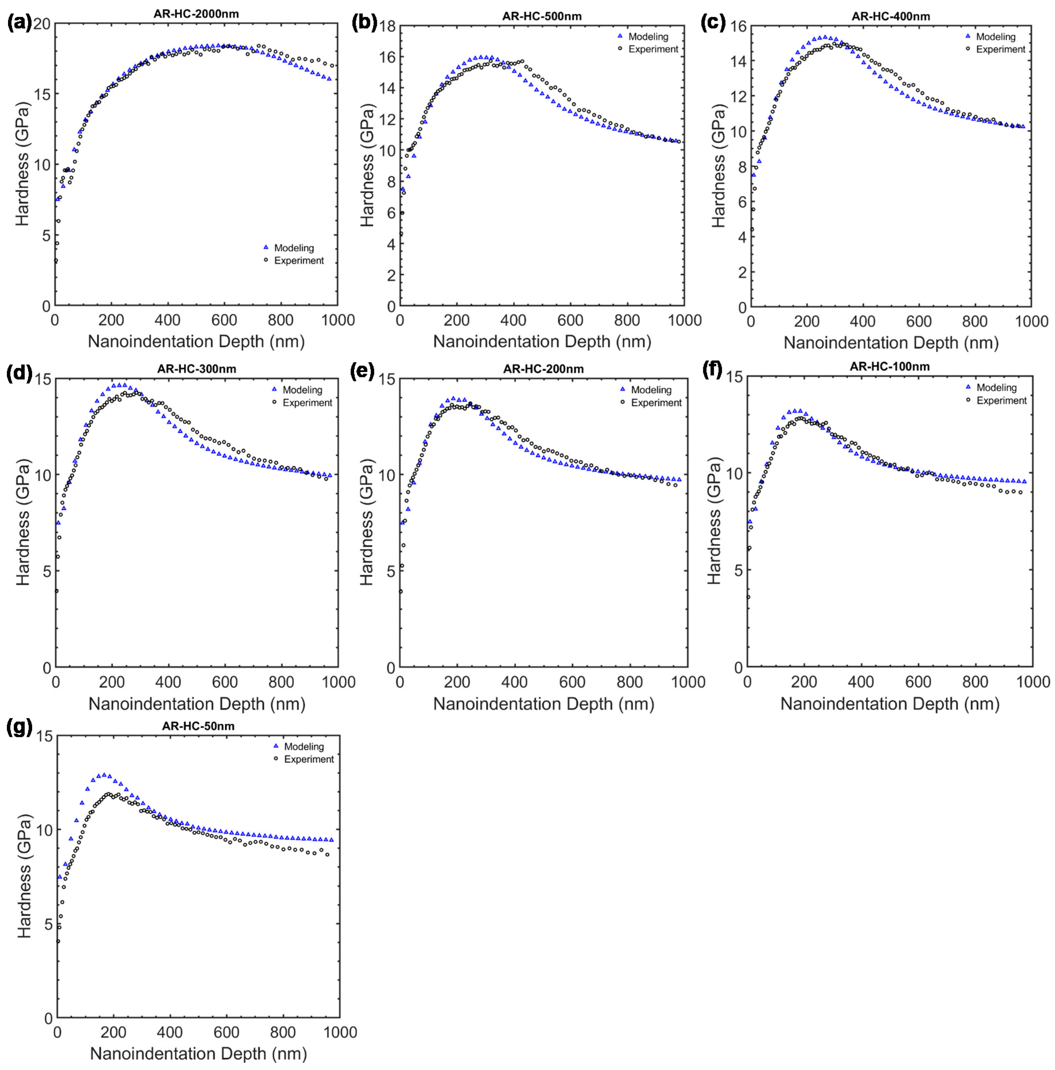
Modeling predictions are compared with experimental data for various stacks, as shown in Figure 9. Overall, the modeling predictions show reasonably good agreement with the experimental data, especially for stacks with thicker H-layers. When the H-layer is only 50 nm (Figure 9g), there is some noticeable difference between the experiment and modeling outcomes. One of the possible reasons for this discrepancy is that the same set of material properties were used for all the numerical simulations. Those material properties were calibrated based on measurements of a single layer coating that has a thickness more than 1 µm. It is likely that a 50 nm H-layer might have different mechanical properties, due to the development of coating microstructure and density during film deposition, as compared to a 2000 nm H-layer. Nevertheless, this analysis shows the capability of FEM to predictively model hardness vs. depth profiles for complex multilayer (here, 13-layer) stacks, starting from single-layer measured experimental data used to establish the input material properties in the FEM model. This can significantly improve the coating stack design exploration and can be readily paired with optical modeling.

3.3.2. Scratch Resistance Testing of AR-HCs

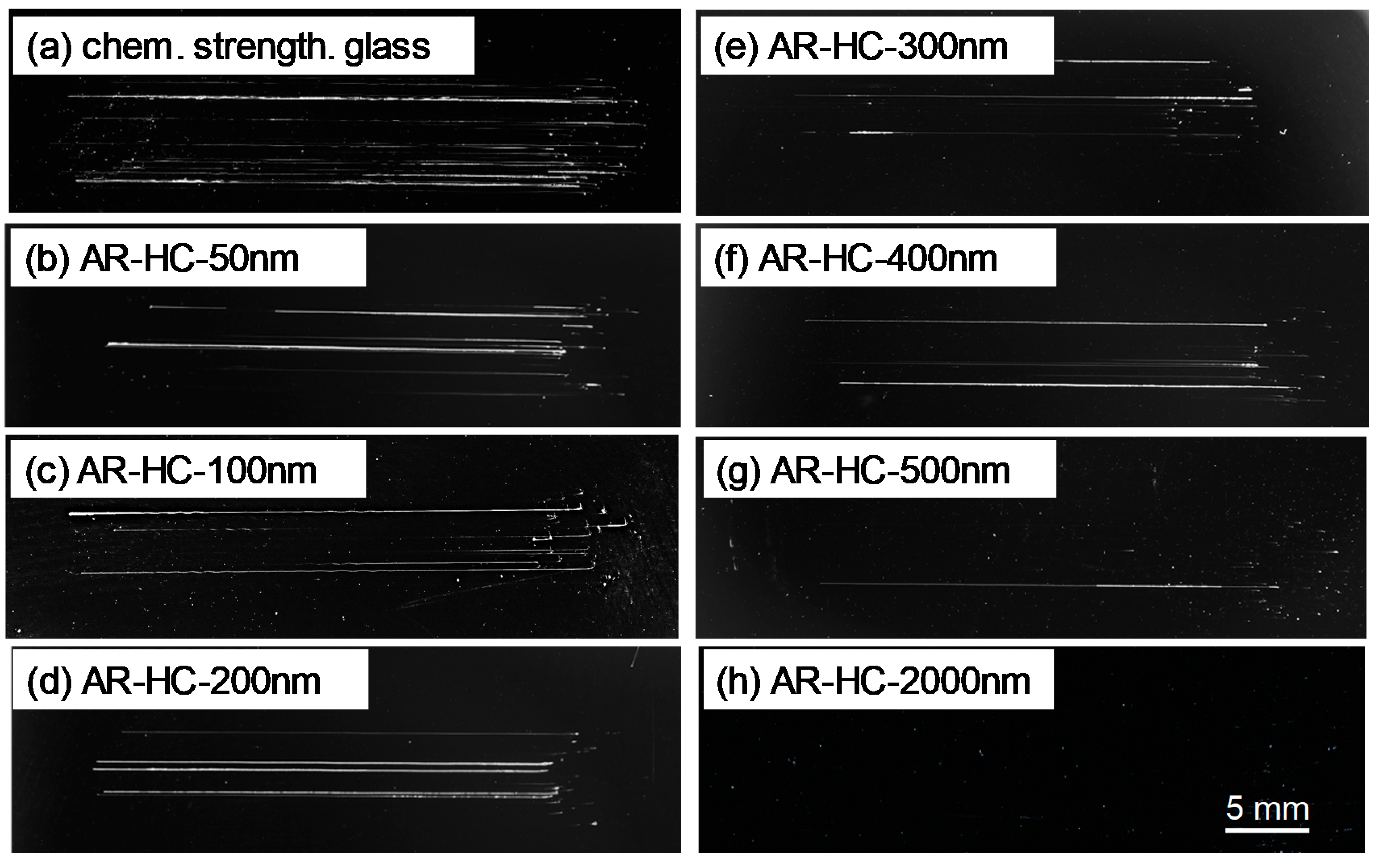
In order to evaluate the practical scratch resistance of the fabricated AR-HCs and compare their hardness profiles to their resistance to simulated real-world surface damage, the previously described Al2O3 abrasion and garnet scratch tests were employed. Both of these tests were found to generate scratches with depths comparable to those found in our field studies, with the garnet scratch test creating damage having the highest similarity to the scratch events observed from the field, due to the single-pass nature of both the garnet scratch test and the observed field scratches. Figure 10 shows optical scattered light images of the AR-HC samples compared to control chemically strengthened glass. From the optical images, it is apparent that the surface durability improves with the increasing hardcoat layer thickness, most notably and consistently for those coatings with an H-layer thickness above ~400 nm and greater (total coating thickness of ~850 nm and greater). This greater coating thickness correlates with hardness sustained at deeper depths as shown through the nanoindentation hardness results above. AR-HC-2000 nm shows particularly excellent durability in this test, with abrasion resistance dramatically exceeding that of the chemically strengthened glass (control sample with no hardcoating).
Abrasion resistance is further quantified in this test using a reflected scattered light measurement (specular component excluded, SCE, reflectance measurement). The results shown in Figure 11 indicate that this method (Al2O3 abrasion + SCE measurement) can be a useful means of quantification, as the trends of increasing abrasion resistance with hardcoat thickness are fairly consistent, correlating with the previously shown nanoindentation hardness vs. depth profiles. The SCE measurement appears to be more definitive when more severe damage is present, and may have more difficulty than the human eye or digital imaging methods in differentiating between samples with relatively lighter damage, such between the AR-HC-500 nm and AR-HC-2000 nm samples. While providing useful quantification of surface durability, it is important to note that the reciprocating abrasion method does not generate the same damage modes as those typically observed in real-world use for consumer electronics (which are single-event scratches).
Figure 12 shows optical scattered light images of the same AR-HC sample series after 1 kg garnet scratch testing. Due to the single-pass nature of this test, which approximates real-world scratch conditions, relatively fewer scratches were created, making the results more noisy and random. Nevertheless the trend of improved scratch resistance is still visible in this test, and the 2000 nm HC layer sample again shows excellent durability in this test, with scratch resistance dramatically exceeding that of the chemically strengthened glass control.
A scattered light quantification method would be noisy and less representative when paired with the single-pass garnet scratch test, due to the relatively random and low number of scratches generated in this test. As such, the garnet scratch severity was quantified through AFM scratch depth measurements for each scratch visible to the naked eye, in the center of the scratch path. Results are shown in Figure 13, giving an indication of both scratch frequency (number of visible scratches) and scratch severity (depth). Of note, the most frequent scratches are in the depth range of those most commonly observed in the field analysis summarized in Figure 1, while a few scratches of greater depth indicate the severity of this test method. The AR-HC samples having an H-layer thickness of 500 nm and greater (total coating thickness of 950 nm and greater) show the clearest reduction in scratch frequency and depth in this test. The AR-HC-2000 nm sample consistently yields zero visible scratches in this test.

4. Discussion

Resistance to micro-ductile deformation/scratching is directly associated with the hardness of the material; higher hardness imparts greater resistance to this type of damage. When using hard coatings to impart scratch resistance, the thickness of the coating (and the resulting hardness vs. depth profile) plays a critical role in deriving the full benefit of the coating. If a coating is too thin, its hardness will not be maintained over a sufficient depth range to prevent moderate to severe scratches in real world scenarios. The contact mechanics responsible for these hardness vs. depth profile effects have been known for some time, but the implications for practical scratch resistant coatings do not appear to have been widely recognized or practiced until very recently [16]. Many attempts to utilize scratch resistant coatings have failed because the critical role of coating thickness has not been fully appreciated—the temptation is to utilize high hardness films that are no more than ~100–200 nanometers thick. The required hardness and thickness levels are intimately related to the nature of the scratching that one is trying to prevent, i.e., the severity of the real-world scratch events that will be encountered in a particular application. Based on analysis and understanding gained from the touch-screen consumer device industry, combined with modeling and experimental analysis of anti-reflection coatings with tunable hardness vs. depth profiles, the types of hardness profiles that are necessary and effective to dramatically reduce moderate to severe scratching in these types of applications are defined in the present work. In particular, coatings with a hardness above ~15 GPa that is maintained over a depth range of ~200–800 nm have been shown to be particularly effective in preventing real-world scratches. The three distinct scratch and abrasion tests utilized here clearly indicate that coatings with depth-of-hardness profiles falling well below these levels are more prone to scratching, and have scratch resistance levels that are close to, or even worse than, chemically strengthened glass. One important factor to keep in mind for anti-reflective coatings is that a scratch with a 50–500 nm depth in an AR coating will typically be much more visible than a scratch of the same depth on uncoated glass, due to the optical interference nature of the coatings which drives high optical contrast between the scratched and unscratched regions. Thus, it is particularly important to minimize scratch frequency in these AR coatings. In order to maintain high hardness over the indicated depth range and nearly eliminate scratching under simulated real-world test conditions, a total coating thickness of ~2.5 microns (with ~2 microns thickness of high-hardness material) has been found to be particularly excellent. The scratch resistance levels for these coatings, exemplified by AR-HC-2000 nm, dramatically exceed those of chemically strengthened glass. For applications with less stringent scratch or damage requirements, anti-reflective hardcoating thicknesses of around ~1 micron (with ~0.5 microns of high-hardness material) have been found to be effective at reducing overall scratch visibility to a level that is moderately better than chemically strengthened glass (which itself is far more scratch resistant than other materials such as polymers).
In addition to the previously described modular opto-mechanical design approach, which enables the fabrication of mechanically tunable optical coatings with nearly invariable optical properties, the utility of additional design and analysis tools is demonstrated here. FEM modeling of hardness was found to adequately predict the hardness vs. depth profiles of multilayer AR-HCs, and this approach can be coupled with optical modeling for multifunctional coating design. Various scratch test methods were evaluated and compared to the trends seen in hardness vs. depth profiles. All of the scratch tests were chosen because they generate scratches of a similar depth and type as those observed in field analysis. These scratch test methods showed a clear trend of agreement with the hardness vs. depth profile analysis—samples with the highest hardness maintained at depths of 500 nm and greater showed especially excellent durability in aggressive scratch and abrasion testing. The garnet scratch test shown here produces scratches that have the greatest similarity to real-world scratches observed in our consumer electronics field trials, however, the single-pass scratch event produces a high level of randomness that makes it more difficult to quantitatively measure the light scattering from these scratches (as compared to the Al2O3 reciprocating abrasion method). Thus, the Al2O3 abrasion method is also useful for quantifying surface damage resistance, due to the ease of quantification through light scattering illustrated here. The diamond nano-scratch method employed is highly precise and useful for developing fundamental understanding, but is less useful for establishing practical real-world durability requirements, due to the fact that diamond is an uncommon abradant in the real world.

5. Conclusions

Mechanically tunable anti-reflective hardcoatings were fabricated, demonstrating the ability to quasi-continuously vary the thickness of a central hardcoat layer in the multilayer stack design, with minimal impact on the anti-reflective optical performance. The fundamentals of hardcoat layer thickness vs. nanoindentation hardness depth profiles were explored through FEM modeling and experimentation. Nanoindentation hardness depth profiles were correlated with practical scratch resistance using three different scratch and abrasion test methods, simulating real world scratch events as observed from consumer electronics field studies. For high practical scratch resistance, coating designs with a hardness of >15 GPa maintained over depths of 200–800 nm, were found to be particularly excellent. The tools and design approaches illustrated here can be extended to create mechanically durable multilayer optical interference coatings of various kinds for multiple applications, including wavelength-selective optics [29], bandpass filters, ophthalmic lenses, IR sensors, and more.

Author Contributions

Conceptualization, K.W.K., L.L., J.J.P., C.A.P., A.M., C.K.W., and S.D.H.; methodology, T.X., B.Z., K.W.K., L.L., J.J.P., E.L.N., K.B.R., and S.D.H.; validation, E.L.N., C.-G.K., D.-G.M., S.-Y.O., J.-K.O., B.Z., K.B.R., and J.J.P.; formal analysis, T.X., K.W.K., L.L., S.D.H., and C.-G.K., investigation, C.-G.K., D.-G.M., S.-Y.O., J.-K.O., C.A.P., T.X., B.Z., and J.J.P.; writing—original draft preparation, J.J.P., T.X., and S.D.H.; writing—review and editing, T.X., S.D.H., and C.K.W.; visualization, T.X., J.J.P., B.Z., and S.D.H.; supervision, J.-H.O., A.M., and C.K.W.; project administration, J.-H.O., A.M., and C.K.W. All authors have read and agreed to the published version of the manuscript.

Funding

This research received no external funding.

Institutional Review Board Statement

Not applicable.

Informed Consent Statement

Not applicable.

Data Availability Statement

The data presented in this study are available on request from the corresponding author.

Acknowledgments

The authors would like to acknowledge Loretta Moses, Jaymin Amin, Jason Harris, Ananth Subramanian, Anthony Furstoss, Leon Reed, Marina Belyustina, Guangli Hu, Heather Decker, Nicholas Walker, Sanjay Sinha, Robert Bellman, John Langstrand, Junghun Yun, Jinah Yoo, Heeseon You, Jiman Lee, Eunhae Ji, Bill McKendrick, Hazel Russell, Arnette Brooks, Brandy Fuller, Phyllis Markowski, Josh Jacobs, Jum Kim, Robert Lee, and Odessa Petzold, for their assistance in experiments, analysis, logistical support, and moral support.

Conflicts of Interest

All authors are employees of Corning Incorporated, which may choose to market or sell technical products related to the subject matter of this article.

References

  1. Macleod, H.A. Thin-Film Optical Filters, 5th ed.; CRC Press: Boca Raton, FL, USA, 2017. [Google Scholar]
  2. Baumeister, P.W. Methods of altering the characteristics of a multilayer stack. J. Opt. Soc. Am. A 1962, 52, 1149–1152. [Google Scholar] [CrossRef]
  3. Southwell, W.H. Coating design using very thin high-and low-index layers. Appl. Opt. 1985, 24, 457–460. [Google Scholar] [CrossRef]
  4. Raut, H.K.; Ganesh, V.A.; Nair, A.S.; Ramakrishna, S. Antireflective coatings: A critical, in-depth review. Energy Environ. Sci. 2011, 4, 3779–3804. [Google Scholar] [CrossRef]
  5. Aiken, D.J. High performance anti-reflection coatings for broadband multi-junction solar cells. Sol. Energy Mater. Sol. Cells 2000, 64, 393–404. [Google Scholar] [CrossRef] [Green Version]
  6. Fink, Y.; Winn, J.N.; Fan, S.; Chen, C.; Michel, J.; Joannopoulos, J.D.; Thomas, E.L. A dielectric omnidirectional reflector. Science 1998, 282, 1679–1682. [Google Scholar] [CrossRef] [PubMed] [Green Version]
  7. Szipöcs, R.; Spielmann, C.; Krausz, F.; Ferencz, K. Chirped multilayer coatings for broadband dispersion control in femtosecond lasers. Opt. Lett. 1994, 19, 201–203. [Google Scholar] [CrossRef] [Green Version]
  8. Weber, M.F.; Stover, C.A.; Gilbert, L.R.; Nevitt, T.J.; Ouderkirk, A.J. Giant birefringent optics in multilayer polymer mirrors. Science 2000, 287, 2451–2456. [Google Scholar] [CrossRef] [Green Version]
  9. Beauchamp, W.T.; Tuttle-Hart, T. UV/IR Reflecting Solar Cell Cover. U.S. Patent 5,449,413, 9 December 1995. [Google Scholar]
  10. Lequime, M. Tunable thin film filters: Review and perspectives. In Proceedings of the SPIE-Optical Systems Design, St. Etienne, France, 30 September 2003; Advances in Optical Thin Films; International Society for Optics and Photonics: Bellingham, WA, USA, 2004; Volume 5250, pp. 302–311. [Google Scholar]
  11. Williams, C.; Hong, N.; Julian, M.; Borg, S.; Kim, H.J. Tunable mid-wave infrared Fabry-Perot bandpass filters using phase-change GeSbTe. Opt. Express 2020, 28, 10583–10594. [Google Scholar] [CrossRef]
  12. Scobey, M.A.; Stupik, P.D. Stable ultranarrow bandpass filters. In Proceedings of the SPIE’s International Symposium on Optics, Imaging, and Instrumentation, San Diego, CA, USA, 7 September 1994; Optical Thin Films IV: New Developments; International Society for Optics and Photonics: Bellingham, WA, USA, 1994; Volume 2262, pp. 37–46. [Google Scholar]
  13. Serényi, M.; Rácz, M.; Lohner, T. Refractive index of sputtered silicon oxynitride layers for antireflection coating. Vacuum 2001, 61, 245–249. [Google Scholar] [CrossRef]
  14. Wang, Y.; Cheng, X.; Lin, Z.; Zhang, C.; Zhang, F. Optimization of PECVD silicon oxynitride films for anti-reflection coating. Vacuum 2003, 72, 345–349. [Google Scholar] [CrossRef]
  15. Hart, S.D.; Koch, K.W.; Paulson, C.A.; Price, J.J. Durable and Scratch-Resistant Anti-Reflective Articles. U.S. Patent 9,335,444, 10 May 2016. [Google Scholar]
  16. Paulson, C.A.; Price, J.J.; Koch, K.W.; Kim, C.-G.; Oh, J.-H.; Lin, L.; Subramanian, A.N.; Zhang, B.; Amin, J.; Mayolet, A.; et al. Industrial-grade anti-reflection coatings with extreme scratch resistance. Opt. Lett. 2019, 44, 5977–5980. [Google Scholar] [CrossRef] [PubMed]
  17. Wang, J.; Bouchard, J.P.; Hart, G.A.; Oudard, J.F.; Paulson, C.A.; Sachenik, P.A.; Price, J.J. Silicon oxynitride based scratch resistant antireflective coatings. In Proceedings of the SPIE Defense + Security, Orlando, FL, USA, 8 May 2018; Advanced Optics for Defense Applications: UV through LWIR III; International Society for Optics and Photonics: Bellingham, WA, USA, 2018; Volume 10627, p. 106270G. [Google Scholar]
  18. Paulson, C.A. Scratch-Resistant and Optically Transparent Materials and Articles. U.S. Patent 10,603,870, 31 March 2020. [Google Scholar]
  19. Musil, J.; Baroch, P.; Vlček, J.; Nam, K.H.; Han, J.G. Reactive magnetron sputtering of thin films: Present status and trends. Thin Solid Films 2005, 475, 208–218. [Google Scholar] [CrossRef]
  20. Rademacher, D.; Zickenrott, T.; Vergöhl, M. Sputtering of dielectric single layers by metallic mode reactive sputtering and conventional reactive sputtering from cylindrical cathodes in a sputter-up configuration. Thin Solid Films 2013, 532, 98–105. [Google Scholar] [CrossRef]
  21. Oliver, W.C.; Pharr, G.M. An improved technique for determining hardness and elastic modulus using load and displacement sensing indentation experiments. J. Mater. Res. 1992, 7, 1564–1583. [Google Scholar] [CrossRef]
  22. Oliver, W.C.; Pharr, G.M. Measurement of hardness and elastic modulus by instrumented indentation: Advances in understanding and refinements to methodology. J. Mater. Res. 2004, 19, 3–20. [Google Scholar] [CrossRef]
  23. Lucas, B.N.; Oliver, W.C.; Swindeman, J.E. The dynamics of depth-sensing, frequency-specific indentation testing. Mat. Res. Soc. Symp. Proc. 1998, 3, 14. [Google Scholar] [CrossRef]
  24. Irland, M.J.; Schermer, E.B. A method for evaluating the abrasion resistance of optical surfaces and thin films. Appl. Opt. 1964, 3, 751–754. [Google Scholar] [CrossRef]
  25. Evans, D.; Zuber, K.; Hall, C.; Griesser, H.J.; Murphy, P. Abrasion resistance of thin film coatings as measured by diffuse optical scattering. Surf. Coat. Technol. 2011, 206, 312–317. [Google Scholar] [CrossRef]
  26. Schneider, J.; Schula, S.; Weinhold, W.P. Characterisation of the scratch resistance of annealed and tempered architectural glass. Thin Solid Films 2012, 520, 4190–4198. [Google Scholar] [CrossRef]
  27. Sun, Y.; Bloyce, A.; Bell, T. Finite element analysis of plastic deformation of various TiN coating/substrate systems under normal contact with a rigid sphere. Thin Solid Films 1995, 271, 122–131. [Google Scholar] [CrossRef]
  28. Care, G.; Fischer-Cripps, A.C. Elastic-plastic indentation stress fields using the finite-element method. J. Mater. Sci. 1997, 32, 5653–5659. [Google Scholar] [CrossRef]
  29. Koch, K.W.; Lin, L.; Price, J.J.; Kim, C.-G.; Moon, D.-G.; Oh, S.-Y.; Oh, J.-K.; Oh, J.-H.; Paulson, C.A.; Zhang, B.; et al. Wavelength-Selective Coatings on Glass with High Hardness and Damage Resistance. Coatings 2020, 10, 1247. [Google Scholar] [CrossRef]
Figure 1. Measured scratch depths of micro-ductile scratches from field study of consumer electronics devices with chemically strengthened glass covers. The majority of observed scratch depths are in the 100–500 nm depth range.
Coatings 11 00213 g001
Figure 2. Schematic illustration of contact mechanics in nanoindentation testing.
Coatings 11 00213 g002
Figure 3. (a) Measured nanoindentation hardness vs. depth for a series of single-layer SiOxNy films of varying thickness coated on aluminosilicate glass substrates. (b) Results of Berkovich diamond tip nano-scratch test on the same single-layer SiOxNy films whose hardness profiles are shown in Figure 3a. Both of the 2000 nm thick films create a >50% scratch depth reduction relative to uncoated chemically strengthened aluminosilicate glass.
Coatings 11 00213 g003
Figure 4. Schematic illustration of fabricated mechanically tunable anti-reflection coatings. Detailed layer design given in inset table.
Coatings 11 00213 g004
Figure 5. First-surface reflectance for series of anti-reflection coating designs depicted schematically in Figure 4, compared to chemically strengthened (CS) glass control sample. The coatings have remarkably similar optical performance, despite their quasi-continuously varying central hardcoat layer thickness. This illustrates the unique level of optical invariance that can be achieved with this design approach.
Coatings 11 00213 g005
Figure 6. Measured nanoindentation hardness vs. depth profiles for series of anti-reflective hardcoatings compared to chemically strengthened (CS) glass control sample. The thickest anti-reflective hardcoatings (AR-HC) maintains high hardness to depths of 1000 nm and beyond, while the thinner AR-HCs have high hardness over a narrower range of depths, and begin to approach the hardness of the CS glass substrate at varying depths from about 500 nm and greater, depending on their thickness.
Coatings 11 00213 g006
Figure 7. Example FEM model used to simulate the nanoindentation of AR-HC coating stacks on chemically strengthened glass substrates. The region of compressive stress in the ion-exchanged (IX) glass is denoted by the depth of the compressive layer (DoC).
Coatings 11 00213 g007
Figure 8. Modeling prediction of 13-layer AR-HC stack on glass indented by Berkovich tip with 100 nm bluntness (a) load vs. depth (b) hardness vs. depth. H-layer thickness ranges from 50 nm to 2000 nm.
Coatings 11 00213 g008
Figure 9. Nanoindentation hardness vs. depth responses of 13-layer AR-HC stacks on glass indented by Berkovich tip with 100 nm bluntness (a) 2000 nm thick H-layer (b) 500 nm thick H-layer (c) 400 nm thick H-layer (d) 300 nm thick H-layer (e) 200 nm thick H-layer (f) 100 nm thick H-layer (g) 50 nm thick H-layer. FEM predictive modeling shows generally good agreement with experimental results, as shown by the comparison of blue (modeling) and black (experimental) curves.
Coatings 11 00213 g009
Figure 10. AR-HC samples abraded with 400 grit Al2O3 sandpaper for 50 cycles with 700 g applied load. Anti-reflective (AR) samples incorporating a hardcoating thickness of ~400 nm or greater clearly show improved abrasion resistance, while the performance is less consistent for samples having a lower thickness and a corresponding shallower depth of high hardness.
Coatings 11 00213 g010
Figure 11. Reflected scattered light (SCE) measurement on Al2O3-abraded AR-HC samples. The trend of increasing abrasion resistance with hardcoat thickness is apparent under these conditions, with samples having H-layer ≥400 nm (total thickness ≥850 nm) performing particularly well in this test.
Coatings 11 00213 g011
Figure 12. AR-HC samples scratched with 150 grit garnet sandpaper for 1 stroke with 1 kg applied load. AR samples incorporating a hardcoating thickness of ~500 nm or greater clearly show improved scratch resistance, while the performance is less consistent for samples having a lower thickness and a corresponding shallower depth of high hardness.
Coatings 11 00213 g012
Figure 13. Depth of scratches visible to the unaided human eye after 1 kg garnet scratch testing, as measured using atomic force microscopy (AFM). AR-HC samples with greater thickness and a corresponding greater depth of high hardness show a reduced frequency of scratches, particularly for samples with H-layer thickness ≥500 nm (total thickness ≥950 nm). Sample AR-HC-2000 nm consistently yields no visible scratches in this test, thus, there are no data points for that sample.
Coatings 11 00213 g013
Table 1. Material properties used as inputs to FEM numerical study.
MaterialYoung’s Modulus (GPa)Poisson’s RatioYield Stress (GPa)
SiOxNy2300.2212.4
SiO2700.224.0
Glass (CS layer)780.224.8
Glass (bulk)720.224.5
Publisher’s Note: MDPI stays neutral with regard to jurisdictional claims in published maps and institutional affiliations.