Abstract
With the increasing interest in dry etching of silicon nitride, utilization of hydrogen-contained fluorocarbon plasma has become one of the most important processes in manufacturing advanced semiconductor devices. The correlation between hydrogen-contained molecules from the plasmas and hydrogen atoms inside the SiN plays a crucial role in etching behavior. In this work, the influences of plasmas (CF4/D2 and CF4/H2) and substrate temperature (Ts, from −20 to 50 °C) on etch rates (ERs) of the PECVD SiN films were investigated. The etch rate performed by CF4/D2 plasma was higher than one obtained by CF4/H2 plasma at substrate temperature of 20 °C and higher. The optical emission spectra showed that the intensities of the fluorocarbon (FC), F, and Balmer emissions were stronger in the CF4/D2 plasma in comparison with CF4/H2. From X-ray photoelectron spectra, a thinner FC layer with a lower F/C ratio was found in the surface of the sample etched by the CF4/H2 plasma. The plasma density, gas phase concentration and FC thickness were not responsible for the higher etch rate in the CF4/D2 plasma. The abstraction of H inside the SiN films by deuterium and, in turn, hydrogen dissociation from Si or N molecules, supported by the results of in situ monitoring of surface structure using attenuated total reflectance-Fourier transform infrared spectroscopy, resulted in the enhanced ER in the CF4/D2 plasma case. The findings imply that the hydrogen dissociation plays an important role in the etching of PECVD-prepared SiN films when the hydrogen concentration of SiN is higher. For the films etched with the CF4/H2 at −20 °C, the increase in ER was attributed to a thinner FC layer and surface reactions. On the contrary, in the CF4/D2 case the dependence of ER on substrate temperature was the consequence of the factors which include the FC layer thickness (diffusion length) and the atomic mobility of the etchants (thermal activation reaction).
1. Introduction
Silicon nitride films have been widely used in the semiconductor industry for applications ranging from passivation layer, anti-reflection layer or advanced electrical devices such as FIN-type transistor, 3D NAND memory, etc. [1]. To prepare the silicon nitride films, many methods are frequently adopted, including low-pressure chemical vapor deposition (LPCVD), plasma-enhanced chemical vapor deposition (PECVD), atomic layer deposition (ALD), plasma-enhanced ALD (PEALD) and chemical reactive rf sputtering, which depend on the property requirements of the applications. Among these methods, PECVD utilizes plasma energy to decompose the precursors, which enable the SiN films to grow at a much lower temperature, by comparing them with the LPCVD. For preparation of SiN films by PECVD, the precursor gases including silane (SiH4), ammonia (NH3) or N2 and other carrier gases such as argon or/and helium are commonly used [2,3]. In general, due to limitations of gas dissociation of the plasma sources, impurities, particularly hydrogen atoms, always reside inside the SiN films which have been considered to influence their physical properties such as optical, electrical and etching behaviors [4,5].
To achieve increased scaling of an electronic device, dry etching process techniques are widely used. In the plasma etching of the SiN films, fluorocarbon or hydrofluorocarbon gases are typically used to alleviate sidewall damage and improve the etching selectivity over the SiO2, Si or other materials [6,7,8,9]. The findings suggested that H in the hydrogen-contained fluorocarbon plasma was crucial in SiN etching. A detailed beam study has reported that the etching chemistries, CxHyFz+, for example, CHF+, CH2F+ and CF2H+ ions significantly affect the etching selectivity [10]. Therefore, the hydrofluorocarbon molecules such as CH2F2 or hydrofluoroethane which energetically prefer to dissociate into CHF2+ or CH2F+ ions have been reported to exhibit superior properties for SiN etching [11,12,13,14].
Substrate temperature (Ts), which inherently affects atomic mobility and reactivity between etchants and film, is one of the important parameters for plasma etching. Cryogenic etching was first invented to enhance the anisotropy etching and reduce plasma damage since the 1980s [15]. It has been reported that the etch rates (ER) of the SiO2, SiNx, Si, etc. films decreased as the Ts decreased, presumably explained by the decrease in fluorine radical reactivity at cryogenic temperature [16,17]. Nevertheless, the ER for fluorine on Si at cryogenic condition has also been reported to be higher due to a denser gas flux on the wafer [18]. On SiO2 etching with SF6 plasma the dramatic decrease in ER has been published when Ts was decreased down to −60 °C [15]. Contrarily, when hydrogen-contained fluorocarbon gas (CHF3) was used, a significant enhancement of ER (a factor of three) was reported when Ts was decreased from 0 to −50 °C, which implied the incorporation of hydrogen and etchants for low temperature or cryogenic etching [19]. On etching of the PECVD-prepared SiN films by the SF6/O2 plasma, a decrease in ER of only ~10% was reported when the Ts was cooled to down to −30 °C [20]. Recently, we reported that the Ts affected ER more significantly in the PECVD-prepared SiN film than in the LPCVD-prepared film, because of the much greater hydrogen content inside the PECVD-prepared films [21]. In addition, the effects of Ts on ERs in two bonding types (Si–H bond rich or N–H bond rich) of the PECVD-prepared SiN films were also addressed [22]. It was discovered that the etching-driven hydrogen dissociation from the different bonding types of the films could give rise to the discrepancy of the fluorocarbon (FC) layer thickness and surface reactions at different Ts.
To elucidate the role of hydrogen sources (inside film and from plasma) and their effects on etching characteristics of the PECVD-SiN thin films, the deuterium gas (D2) was added to CF4 plasma to etch the SiN films with Si–H bond rich structure [23]. However, the etching mechanism for the SiN films by the CF4/D2 plasma is still unclear. In this work, a detailed comparison on Ts-dependent ER, surface structure and reactions was made with the CF4/H2 plasma. It was demonstrated that the ER for the CF4/D2 plasma were higher than that of for the CF4/H2 plasma [23]. The higher ER in the CF4/D2 plasma cannot be explained by the results of plasma density (ne), gas phase concentration and FC thickness. The mass effect and energy transfer was considered to partially contribute the ER increase with D2 addition. The experiment concerning H abstraction by D2 plasma supports the statement that H dissociation from the films is important for the PECVD-prepared SiN films when the hydrogen concentration inside the films is high.
2. Experimental Section
A dual frequency capacitively coupled plasma (CCP) reactor with a very high frequency (VHF) of 100 MHz and on a top electrode and low frequency (LF) of 2 MHz on a bottom electrode was used in this work. The background pressure before plasma ignition was lower than 5 × 10⁻⁴ Pa. The plasma was generated by the VHF power, up to 300 W, applied to the top electrode and bias was induced by the bottom electrode with LF power of 200 W for the etching experiments. The electrode gap was 30 mm and the substrate diameter was 100 mm. The SiN coupon (10 × 10 × 0.5 mm3) was fixed on a Si substrate using fluorinated grease to improve the thermal conductivity between the samples and a Si substrate. The Si substrate was set on the bottom electrode with an electrostatic chuck. The Ts was controlled from −20 to 50 °C by a coolant circulation system in the bottom electrode. A He backflow with a pressure higher than 700 Pa was set to improve the thermal conductivity between the chuck and the Si substrate. A mixture of gases from CF4 and D2 (or H2) with a flow ratio of 2:1 was introduced through showerhead distributor installed at the upper electrode. The working pressure was fixed at 4.0 Pa.
The PECVD-prepared SiN thin films with a Si–H bonding-rich structure were prepared in this work. The structural and chemical properties of the films were analyzed with various thin film characterizations, including Fourier-transformation infrared spectroscopy (FTIR), Rutherford backscattering spectroscopy/hydrogen forward scattering spectroscopy (RBS/HFS), and X-ray reflectivity (XRR). As shown in Table 1, the chemical composition of the film was examined to be Si39.2N41.3H19.5 (±0.2 at.%) with the RBS/HFS technique (National Electrostatics Corporation, Pelletron 3SDH). The peak area ratio of the Si-H over N–H bonding absorption was calculated to be 5.6 from the FTIR (Nicolet iS50, Thermo Scientific, Waltham, MA, USA). The film density of 2.30 g/cm3 was confirmed from the XRR (Rigaku, ATX-G, Hokuto, Japan). The film thickness was measured by using in situ spectroscopic ellipsometry (SE, M-2000F, JA Wollam, Lincoln, NE, USA) over a wavelength range from 300 to 1000 nm with an incident angel of 75°.

Table 1.
Film thickness, chemical composition, mass density and ratio of Si-H over N-H bonding of the PECVD-prepared SiN films before etching.
The ER was determined by the thickness change during etching, calculated by an average thickness change of 10 s. An optical model with the Tauc-Lorentz oscillators was used to fit the SE data. All optical parameters were fixed during plasma etching, and only the film thickness was fitted. The surface chemical structure and the film composition were characterized by X-ray photoelectron spectroscopy (XPS, XPS-1600, Ulvac-Phi, Chigasaki, Japan) with a monochromatic Al Kα beam. To examine the depth-dependent structure of the films the spectra were obtained at different take off angles (TOA), so-called angular resolved XPS. The Shirley function was adopted to remove the background of the XPS data before peak deconvolution. A combination of Gauss and Lorentz shape peak function (Voigt) function was used for peak deconvolution.
To verify whether the X-H (X = Si or N) bonds were being abstracted by deuterium, a 30 nm thick SiN film deposited on a Ge prism (20 × 80 × 1 mm3) as a sample to be etched was firstly treated by pure H2 plasma for 5 s, and followed by pure D2 plasma for 5 s. The substrate temperature was set at 20 °C. Note that the bonding structure of the film for this experiment was not identical to the films etched by CF4/H2(D2) mentioned above, but the high hydrogen content inside the film was confirmed (22.7 at.%) by the RBS. Surface modification was assessed by in situ attenuated total reflection (ATR)-FTIR (Nicolet8700, Thermo Scientific). The spectra were recorded in the range of 600–4000 cm−1 with a resolution of 4 cm−1; however, due to the strong absorption of SiN, the cutoff of absorbance signal was approximately 1000 cm−1. The surface morphology of the samples was observed by the atomic force microscopy (AFM, Bruker AXS Dimension3100, Billerica, MA, USA).
The gas phase of the plasmas was qualitatively monitored with optical emission spectroscopy (OES, HR2000+, Ocean optics, Orlando, FL, USA) with the wavelength range of 200–900 nm and resolution of 0.5 nm. The OES was observed through a quartz window mounted on the reactor chamber wall. The plasma densities of the CF4/D2 and CF4/H2 plasmas at different power inputs range from 50 to 300 W of the top electrode were analyzed by a plasma absorption probe (PAP, Home-made) [24,25,26]. A quartz tube with an outer diameter of 5 mm was inserted through the reactor. The tip of the probe was set at the center and 15 mm above the bottom electrode.
3. Results
3.1. Plasma Diagnostics
Figure 1a shows the representatives of reflection spectra obtained by PAP of the CF4/H2 plasma at upper electrode inputs of 100 and 300 W. The reflection intensity was obtained as a function of frequency. The resonant absorption occurs when surface wave resonance frequency is closed to plasma oscillation. Accordingly, we can obtain the absolute electron density by the following formula, ne = 1.24 × 10¹⁰ fabs2 cm−3, where fabs is determined by peak fitting of the spectrum in unit of GHz [24]. The dependences of ne on the power input of upper electrode of the CF4/D2 and CF4/H2 plasmas were illustrated in Figure 1b. As expected, the ne increased monotonically with the power input, and reached to the maximum value of ~1.54 and 1.58 × 1011 cm−3 for the CF4/D2 and CF4/H2 plasma at 300 W, respectively. There was no significant difference on the electron density between these two plasmas. Additionally, we also found that the electron density was insensitive to the variation of Ts (within statistical error, not shown).
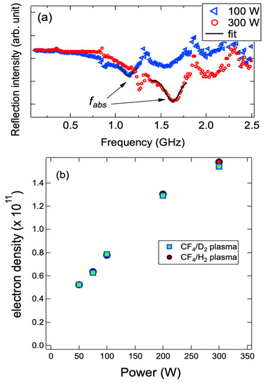
Figure 1.
(a) Representative resonance spectra observed by the surface wave probe for the CF4/H2 plasma at different power inputs of the upper electrode; (b) dependences of electron densities (ne) of the CF4/D2 and CF4/H2 plasma at the different power inputs.
The OES spectra of CF4/D2 and CF4/H2 plasmas acquired at Ts = 50 °C are plotted in Figure 2. The inset of Figure 2a shows the peak of the Balmer line D(H) around 486 nm of the plasmas, indicating that the intensity of the Dα in the CF4/D2 plasma was approximately 19% greater than that of Hα in the CF4/H2 plasma. This result is consistent with the previous works which have reported a larger cross-section of rotational excitation of D2 than that of H2 [27,28]. Likewise, the intensities of FC species (~300–450 nm) and F emissions of the CF4/D2 were higher than ones obtained by the CF4/H2 plasma, as shown in Figure 2b,c. The results imply that the concentrations of D, FC and F in the CF4/D2 plasma were greater than that in the CF4/H2 plasma, because the emission processes of D2 can be presumably considered to be identical to those in H2. Furthermore, the OES spectra shown in this work were very similar to that obtained at Ts = 20 °C as shown in the Ref. [23], indicating that the gas phase species were insensitive to the Ts variation.
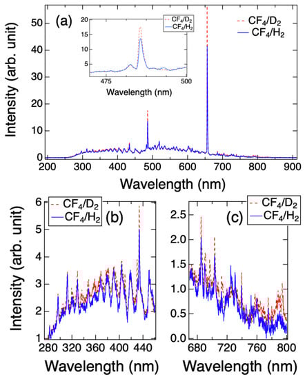
Figure 2.
(a) OES spectra of the CF4/D2 and CF4/H2 plasmas at Ts = 50 °C. The inset of the (a) shows the wavelength range from 470 to 500 nm for Balmer line D(H)α. The specific wavelength ranges for FC and F emissions were plotted in (b) and (c), respectively.
3.2. Etching Characteristics
Figure 3 illustrates the dependences of etch rate on Ts for the films etched by the CF4/D2 and CF4/H2 plasmas, also presented in Ref. [23]. For the CF4/D2 plasma, the ER initially increased gradually from 3.4 to 4.0 nm/s as Ts was decreased from 50 to 20 °C, and then it decreased to 3.0 nm/s at Ts = −20 °C. On the contrary, for the CF4/H2 plasma the ERs were around 1.5 nm/s in Ts range from 50 to 20 °C, and the value increased dramatically to 3.2 when Ts was cooled down to −20 °C. This has been interpreted by the fact that the low temperature led to the formation of N–H favored upon the exposure of the CF4/H2 plasma which was likely to accelerate the H dissociation from the SiN films via some surface reactions and enhance the ER [22]. Overall, the ERs of the CF4/D2 plasma were higher than that of the CF4/H2 plasma, except for Ts = −20 °C at which the ERs were closed.
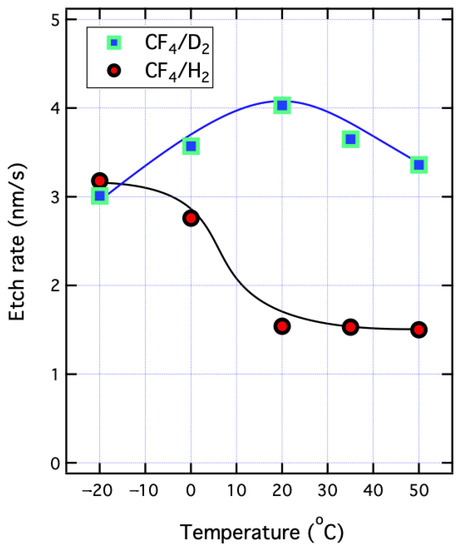
Figure 3.
Dependence of etch rates on substrate temperature of the PECVD-prepared SiN films proceeded with the CF4/D2 and CF4/H2 plasmas. Reprinted with permission from Ref. [23], 2020, IEEE.
Figure 4 shows the C 1s XPS spectra of the SiN etched by the CF4/D2 and CF4/H2 plasmas at different Ts. The merge of peaks referred to the carbon to carbon/fluorine bonding (C-C, C-CFx, C-CF, C-CF2, C-CF3) that was clearly observed and deconvoluted. Due to the more electronegative nature of fluorine, the bonds with more fluorine atoms that are in molecules, the greater the positive shift of binding energy from C-C band. For the SiN etched by CF4/D2 plasma, the strong C-CF molecule peaks (CF3, CF2 and CF1) were found. On the contrary, for the CF4/H2 plasma the spectra exhibited a strong component for C-C bonding. These results indicate that the structure of the FC layer formed on the SiN films by the CF4/D2 plasma was different from the CF4/H2. Additionally, from the peak intensity, it can be deduced that the FC thickness formed by the CF4/D2 plasma was thicker than that by CF4/H2 plasma. To determine the FC layer quantitatively, a non-destructive method based on Beer–Lambert equation and the angular-resolved XPS was used [29,30]. In this study, the intensity ratio of Si 2p core level at different TOAs (90 and 15 or 20°, depending on FC thickness) was used to determine the FC layer thickness, dFC, by the following formula:
where λ represents the electron inelastic mean free path (IMPF) of the FC layer. The λ for the FC layer is given as 3.2 nm from the published data [31,32]. ISi 2p and I′Si 2p are denoted as the total intensity of the Si 2p peak at each TOA. The FC thicknesses on the SiN film etched by the CF4/D2 and CF4/H2 plasmas as a function of Ts are shown in Figure 5a. It can be clearly seen that for both plasmas the FC thicknesses were thicker than 2.5 nm and decreased as Ts decreased from 50 to −20 °C. At all Ts, the FC thickness on the SiN films etched by the CF4/D2 plasma was thicker than that by the CF4/H2 plasma. To understand the structure of the FC polymer, the F/C ratio was determined by the following equation:
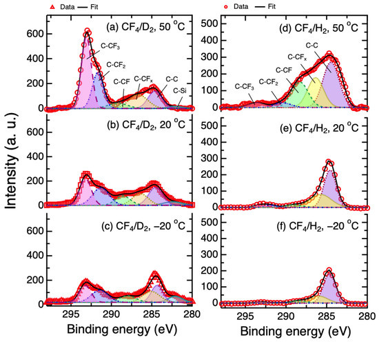
Figure 4.
Carbon 1s XPS spectra of the SiN etched by CF4/D2 plasma at Ts = (a) 50 °C; (b) 20 °C and (c) −20 °C, and CF4/H2 plasma at (d) 50 °C; (e) 20 °C and (f) −20 °C. The TOA was fixed at 90°.
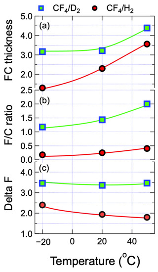
Figure 5.
(a) thickness; (b) F/C ratio and (c) ∆F of the fluorocarbon layer on the surface of the SiN films etched by the CF4/D2 and CF4/H2 plasmas at different substrate temperatures. ΔF is defined as the difference of the ratio of the XPS F1s/C1s intensity and the F/C ratio, indicating a measure for “fluorination of SiN film”.
As illustrated in Figure 5b, for the CF4/D2 plasma case the F/C ratio was found to be greater than unity, and decreased from 2.00 to 1.17 as Ts was decreased from 50 to −20 °C. On the other hand, when the CF4/H2 plasma was used, the FC layers on the etched SiN films exhibited the F/C ratios less than 0.5, less amenable to Ts. Furthermore, because F is the main etchant element for etching SiN by fluorocarbon-based plasmas, it would be informative to estimate the amount of F located in the SiN films. Here, a measure called ΔF is defined, which is calculated by a difference of the ratio of F1s/C1s intensity and the F/C ratio determined by Equation (2), i.e., ΔF = F1s/C1s − F/C [33]. The magnitude of ΔF, therefore, is an indication of “SiN layer fluorination”. When ΔF increases, it indicates that relatively more of the F is bonded with the Si rather than existing in the FC layer. Figure 5c shows the dependence of ΔF on Ts by the CF4/D2 and CF4/H2 plasmas. The ΔF of the SiN films etched by CF4/D2 plasma were obtained to be ~3.5 and unvaried with Ts, which are much greater than the obtained (~2) by the CF4/H2 plasma. In addition, for the CF4/H2 plasma case ΔF was increased as Ts decreased.
The surface morphology of the samples before etching, and after etching with the CF4/D2 and CF4/H2 plasmas at Ts of 20 °C was described in Supplementary Materials.
4. Discussion
From the above results, one can notice the following facts: (1) the ER obtained by the CF4/D2 plasma was higher than that by the CF4/H2; (2) The greater concentrations of the gas phase active species (FC, F and D) in the CF4/D2 plasma; (3) The FC thickness, F/C value and ΔF in etched SiN film by the CF4/D2 are higher than those obtained by the CF4/H2 plasma.
4.1. FC Polymer and Surface Reactions
The FC polymer is one of the most important factors in determining the ER by using fluorocarbon-containing plasma. Under steady-state circumstances of continuous etching, the FC thickness is determined by a balance between consumption by ion bombardment, etch reaction and deposition of FC layer. A thick FC layer usually acts an “inhibitor” or even a “stopper”, if too thick, for etching; meanwhile, it also plays the role of etchant supplier when the F can be released from FC molecules under ion bombardment. Accordingly, the structures and thickness of the FC layers are amenable to the nature of plasmas, outfluxes from the films during etching and internal environment of reactor [34,35]. Generally speaking, the H-containing plasma usually leads to high polymer deposition rates, because H atoms can scavenge the F atoms to form HF molecules which cause the fluorine-poor condition, especially for Si or SiO2 etching [36,37]. However, in SiN etching H atoms play a role of etchant which can react with C and N atoms to form HCN byproducts. Hence, in some certain conditions, the thinner FC polymers have been reported in the hydrofluorocarbon plasmas [10,21,38]. In this work, we observed that for the CF4/H2 plasma the films exhibited the thinner thickness than that for the CF4/D2 plasma. This could be result of the higher FC gas species observed by the OES (Figure 2c), although the H2 has been reported to exhibit a higher reaction cross section with F than that of D2 [39,40].
In previous literature, it has been explored and is well known that the overall etch rate of the Si-based materials scales inversely with the amount of the FC thickness [41,42,43]. However, it is most likely that the FC thickness was not responsible for the higher ER in the CF4/D2 plasma, due to the fact that the thicker FC layer was observed at all Ts. Because the FC thickness (>2.5 nm) on the SiN films etched by the plasmas were much thicker than 1 nm (see Figure 5a), one could expect that the incoming ions (except for the D(H)+ ion) were unable to penetrate FC layer and their energies were transferred to the upper part of the FC film. This gives rise to the release of etchants such as F for Si, and C for N by formation of CN molecule from the fragmentation of the FC layer which is being ion bombarded. In this case, the ER, therefore, strongly depends on the diffusion rates of the etchants. This can explain the fact that the higher ΔF of the SiN films etched by the CF4/D2 plasma also exhibited a higher ER than that by the CF4/H2 (see Figure 5c). The F etchants which were removed from the FC film under ion bombardment moved toward to the SiN film by a thermal diffusion process and, then, reactions with Si took place.
By comparing the amounts of F/C and ΔF, one may notice the fact that the overall presence of F, including the FC layer and fluorinated SiN, in the samples proceeded by the CF4/H2 plasma was smaller than by the CF4/D2. As mentioned in our earlier publication, the greater hydrogen outflux and H atoms from the gas phase scavenges the F radicals to form HF molecules [22]. Due to the thicker FC layer and lower reactivity of F with D [39,40], a lower amount of H(D)F molecules is expected in the case of the CF4/D2, which also leads to the higher ER and overall presence of F.
4.2. Mass Effect
From the OES results, one may expect the higher F concentration could contribute to the higher ER. However, the intensity of the F emission for the CF4/D2 plasma was only 17% stronger than that for the CF4/H2 plasma. This may fail to explain the dramatic increase in the ER with D2 addition to CF4. The D2 plasma has been reported to enhance the ER of Si but at the same time showed no effect on the SiO2 etching [44], suggesting that the mass effect and the resultant transfer energy could lead to the bonding break of the weak Si-Si bonds but may be insufficient for the strong Si–O bonds. Since the bonding energy for Si-N (~3.5 eV) is stronger than that of Si–Si but weaker than Si-O (~4.8 eV) [45], the mass effect of D may contribute to the ER. However, the relatively weak mass effect on the Si3N4 etching has also been reported [46], although the film properties and the etching condition have not been addressed in detail. Furthermore, due to the strong bonding energy of C-F (~5.6 eV) [47], the mass effect is most likely to have no impact on the release of the F.
Consequently, in the present study the thicker FC layer; as a protective layer, deposited on the SiN films by the CF4/D2 plasma is expected to reduce the mass effect.
4.3. Hydrogen Abstraction by Deuterium and Etching Model
In the earlier study, the D2 plasma was discovered to abstract the hydrogen inside the amorphous hydrogenated Si film and further led to an etching reaction [48]. Recently, the H dissociation of the PECVD-prepared SiN films with high H content (~20 at.%) has been reported to play an important role in determining the etching process with the hydrogen-containing fluorocarbon plasmas [22,38,49]. Because the SiN films prepared in this work exhibit a very high H content inside the films (~20 at.%), the abstraction of H inside the films with deuterium in the CF4/D2 discharge can be expected. To support this hypothesis, the SiN film deposited on a Ge prism was firstly treated with the H2 plasma, and then followed by the D2 plasma; simultaneously, the ATR-FTIR was used to in situ monitor the variation of chemical bonding of the film. All spectra acquired with respect to the references before plasma treatment show only the differences in absorbance in the film due to reactions with H or D from the discharges. Figure 6 presents the absorbance spectra obtained in the SiN film treated by the H2 and D2 plasmas. There was no observable change in the IR spectrum when the film was treated with H2 plasma for 5 s. On the contrary, upon exposure to the D2 plasma even only for 1 s, the D replaced H in the films which led to the formation of Si-D stretching modes appears at ~1580 cm−1 and -NDx at 2500 cm−1 and the corresponding decrease in Si-H at ~2100 cm−1 and -NHx at ~3300 cm−1. When the D2 exposure time was increased from 1 to 5 s, a significant change in absorbance was found for the increase in Si–D and -NDx, and, in the meantime, the decrease in Si–H and -NHx modes. These data provide unambiguous evidence of the H abstraction by the D2 plasma in the highly hydrogenated SiN film. As a consequence, the following reactions are likely to take place [45]:
Si-H + D → Si-D + H ΔE = −0.8 eV
Si-D + N-H → Si-N + H-D ΔE = −1.86 eV
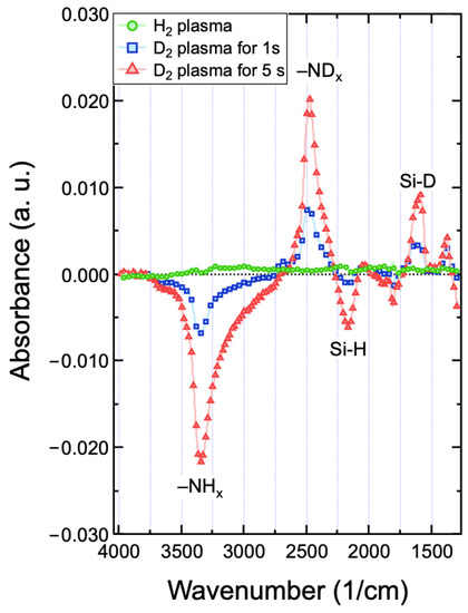
Figure 6.
In situ ATR-FITR spectra of the SiN film deposited on a Ge prism with treatment of H2 plasma for 5 s, and followed by D2 plasma for 1 and 5 s.
A model for mechanism of SiN etching by CF4/D2 plasma is proposed, as illustrated in Figure 7a. From the FC thickness results, a thick FC polymer is deposited on the surface of the SiN film. Due to the high penetration of D, the abstraction of hydrogen by deuterium take places. The resultant Si–D bonds can react with the N–H bonds of the films through Equation (4). The dissociation of H by forming H–D molecules will result in a higher reaction probability of F and C etchants which are generated by ion bombardment on the FC polymer to react with Si or N dangling bonds [38,50], as illustrated in Figure 7a. This is consistent with the finding of the higher ∆F for the CF4/D2 plasma (see Figure 5c), indicating a higher fluorination state of the SiN surface. Finally, the volatiles such as SiF4, HCN and/or FCN are liberated when etching is proceeding [21]. In contrast, in the CF4/H2 plasma (Figure 7b), as proposed in Ref. [22], the H dissociation preferentially take place via formation of HF or HCN molecules instead of H2 or NH3, according to the computational chemistry calculations and/or experiments [38,51]. A higher HF amount in the CF4/H2 plasma because of the scavenge of F atoms results in an overall lower ER and, as a consequence, lower probabilities for the volatile byproducts.
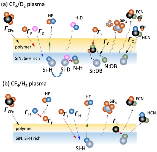
Figure 7.
Schematic illustration of the proposed etching mechanism of the SiN film etched by the (a) CF4/D2 plasma and (b) CF4/H2 plasma.
4.4. Effect of Ts
Substrate temperature is an intrinsic factor which will influence the physical and chemical properties of materials. The dependences of ER on Ts have also been reported in many systems with different materials and etching conditions [15,16,17,18,20,52]. In our previous works, we found that the Ts had more impact on ER when the hydrogen content of the SiN films was higher [21]. The increase in ER in the SiN films at low temperature by using the CF4/H2 plasma, as shown in Figure 3, has been attributed to one or more of the following factors: FC thickness, surface reactions and thermal mobility of etchants [22]. Here, it is interesting to note that the reactions at low temperature for the CF4/H2 plasma, i.e., Si-H + N-H → Si-N + H2, as described in the Ref. [22], basically, are the counterpart of Equation (4) for H dissociation. Therefore, the ER obtained by the CF4/H2 at low temperature increased to a value close to that of CF4/D2 (see Figure 3). On the other hand, in the CF4/D2 case, because of the thick FC layers (>3.2 nm), as discussed before, the etching mechanism is considered to be an ion-induced defluorination process, i.e., the ER strongly depends on the how the fluorine atoms are released (generation) by ions which imp on the FC layer and move towards the SiN layer (transportation); in particular, Si or N dangling bonds. We believe that the thermal effect on the generation of fluorine is negligible, although the peak to peak voltage of the bias electrode was measured to be approximately 1.55 kV in the CF4/D2 plasmas. Hence, a fluorine diffusion-controlled etching process depending on fluorine mobility (thermal-driven reaction) and diffusion length (FC thickness) can be expected. The reactivity of fluorine with Si has been reported to be insensitive to Ts range of 20 to −100 °C concerning no deposition on top of the Si [53]; however, the diffusion process of fluorine atoms through a polymer film, if it exists, would strongly depend on thermal activation energy [54]. In this case, the effect of Ts on atomic diffusion should not be neglected. A presumable explanation of the variation of ER on Ts for the CF4/D2 plasma is as follows: as shown in Figure 5a, when Ts was −20 °C, the combination of the thinner FC layer (shorter diffusion length) and lower atomic mobility due to low temperature led to the relatively low ER; on the contrary, for Ts at 50 °C, the combination of the thicker FC layer (longer diffusion length) and high atomic mobility due to high temperature also caused the relatively low ER. Accordingly, there was a maximum value of ER at 20 °C, at which a well-balance of the appropriate diffusion length and atomic mobility was made. This is probably the reason why the ER decreased as Ts was decreased from 50 to 20 °C, and then it decreased again as the Ts was further decreased to −20 °C.
5. Conclusions
We demonstrated and discussed the etching characteristics of the PECVD-prepared SiN films with the CF4/D2 and CF4/H2 plasmas at substrate temperatures varied from −20 to 50 °C. The ER of the SiN films etched by the CF4/D2 plasma was higher than that by the CF4/H2 plasma. The fluorocarbon film thickness, gas phase active species concentration and plasma density cannot explain the higher ER in the CF4/D2 plasma. The in situ monitoring of surface structure change in the SiN film with the H2 and D2 plasma indicates that the hydrogen inside the film can be replaced by deuterium, which probably lead to a series of surface reactions to form Si and N dangling bonds. A model based on the hydrogen abstraction by deuterium which leads to a higher reaction probability of the etchants (F, C or D) between Si and N dangling bonds is proposed. For the CF4/H2 plasma, the ER significantly increased as Ts decreased, which has been explained by the thinner FC layer and the H dissociation as well as the resultant reactions. On the contrary, for the CF4/D2 plasma, the dependence of ER on Ts was determined by the summation of effects of the FC thickness and atomic mobility of the etchants. The results suggest that H dissociation is one of key factors in determining etch behavior for a SiN with high H concentration, particularly for the PECVD-prepared SiN film. The findings in this work not only present important scientific concepts on fundamentals but also provide useful insights for the development of etching process for practical applications.
Supplementary Materials
The following are available online at https://www.mdpi.com/article/10.3390/coatings11121535/s1, Figure S1: Surface roughness of the samples (a) before etching and after etching with the (b) CF4/D2 and (c) CF4/H2 plasma at substrate temperature of 20 °C.
Author Contributions
Conceptualization, S.-N.H.; methodology, S.-N.H.; software, S.-N.H.; validation, S.-N.H. and M.S.; formal analysis, T.-T.-N.N.; investigation, S.-N.H.; resources, T.T. and K.I.; data curation, S.-N.H., T.-T.-N.N.; writing—original draft preparation, S.-N.H.; writing—review and editing, M.S. and M.H.; visualization, S.-N.H.; supervision, M.S. and M.H.; project administration, M.S.; funding acquisition, M.H. All authors have read and agreed to the published version of the manuscript.
Funding
This research received no external funding.
Institutional Review Board Statement
Not applicable.
Informed Consent Statement
Not applicable.
Data Availability Statement
Data are contained within the article or supplementary material.
Acknowledgments
The authors would like to thank Hiroki Kondo for fruitful discussions and Liugang Hu for the measurement of surface roughness.
Conflicts of Interest
The authors declare no conflict of interest.
References
- Kaloyeros, A.E.; Pan, Y.; Goff, J.; Arkles, B. Review-Silicon nitride and silicon nitride-rich thin films technologies: State-of-the-art processing technologies, properties, and applications. ECS J. Solid Sci. Tech. 2020, 9, 063006. [Google Scholar] [CrossRef]
- Sahu, B.B.; Yin, Y.Y.; Tsutsumi, T.; Hori, M.; Han, J.G. The role of plasma chemistry on functional silicon nitride film properties deposited at low-temperature by mixing two frequency powers using PECVD. Phys. Chem. Chem. Phys. 2016, 18, 13033. [Google Scholar] [CrossRef] [PubMed]
- Jonas, S.; Janus, M.; Jaglarz, J.; Kyziol, K. Formation of SixNy(H) and C:N:H layers by plasma-assisted chemical vapor deposition method. Thin Solid Films 2016, 600, 162. [Google Scholar] [CrossRef]
- Prccirillo, A.; Gobbi, A. Physical-electrical properties of silicon nitride deposited by PECVD on III-V semiconductors. J. Electrochem. Soc. 1990, 137, 3910. [Google Scholar] [CrossRef]
- Lin, K.-C.; Lee, S.-C. The structural and optical properties of a-SiNx:H prepared by plasma enhanced chemical vapor deposition. J. Appl. Phys. 1992, 72, 5474. [Google Scholar] [CrossRef]
- Kuo, Y. Reactive ion etching of PECVD amorphous silicon and silicon nitride thin films with fluorocarbon gases. J. Electrochem. Soc. 1990, 137, 1235. [Google Scholar] [CrossRef]
- Li, Y.X.; French, P.J.; Wolffenbuttel, R.F. Selective reactive ion etching of silicon nitride over silicon using CHF3 with N2 addition. J. Vac. Sci. Tech. B 1995, 13, 2008. [Google Scholar] [CrossRef]
- Kumar, M.J.; Chamberlain, S.G. Selective reactive ion etching of PECVD silicon nitride over amorphous silicon in CF4/H2 and nitrogen containing CF4/H2 plasma gas mixtures. Solid State Electron. 1996, 39, 33. [Google Scholar] [CrossRef]
- Ohtake, H.; Wanifuchi, T.; Sasaki, M. SiN etching characteristics of Ar/CH3F/O2 plasma and dependence on SiN film density. Jpn. J. Appl. Phys. 2016, 55, 086502. [Google Scholar] [CrossRef]
- Ito, T.; Karahashi, K.; Fukasawa, M.; Tatsumi, T.; Hamaguchi, S. Hydrogen effects in hydrofluorocarbon plasma etching of silicon nitride: Beam study with CF+, CF2+, CHF2+, and CH2F+ ions. J. Vac. Sci. Tech. A 2011, 29, 050601. [Google Scholar] [CrossRef]
- Kondo, Y.; Ishikawa, K.; Hayashi, T.; Miyawaki, Y.; Takeda, K.; Kondo, H.; Sekine, M.; Hori, M. Silicon nitride etching performance of CH2F2 plasma diluted with argon or kypton. Jpn. J. Appl. Phys. 2015, 54, 040303. [Google Scholar] [CrossRef]
- Miyoshi, N.; Shinoda, K.; Kobayashi, H.; Kurihara, M.; Kouzuma, Y.; Izawa, M. Atomic layer etching of Si3N4 with high selectivity to SiO2 and poly-Si. J. Vac. Sci. Tech. A 2021, 39, 052601. [Google Scholar] [CrossRef]
- Hayashi, T.; Ishikawa, K.; Sekine, M.; Hori, M. Electronic properties and primarily dissociation channels of fluoroethane compounds. Jpn. J. Appl. Phys. 2019, 58, SEEF01. [Google Scholar] [CrossRef]
- Hsiao, S.N.; Ishikawa, K.; Hayashi, T.; Ni, J.; Tsutsumi, T.; Sekine, M.; Hori, M. Selective etching of SiN against SiO2 and poly-Si films in hydrofluoroethane chemistry with a mixture of CH2FCHF2, O2, and Ar. Appl. Surf. Sci. 2021, 541, 148439. [Google Scholar] [CrossRef]
- Tachi, S.; Tsujimoto, K.; Okudaira, S. Low-temperature reactive ion etching and microwave plasma etching of silicon. Appl. Phys. Lett. 1988, 22, 616. [Google Scholar] [CrossRef]
- Pearton, S.J.; Abernathy, C.R.; Ren, F.; Lothian, J.R.; Kopf, R.F. Low-temperature dry etching of Tungsten, dielectric, and trilevel resist layers on GaAs. Plasma Chem. Plasma Proc. 1993, 14, 505. [Google Scholar] [CrossRef]
- Flamm, D.L.; Donnelly, V.M.; Mucha, J.A. The reaction of fluorine atoms with silicon. J. Appl. Phys. 1981, 52, 3633. [Google Scholar] [CrossRef]
- Tinck, S.; Tillocher, T.; Dussart, R.; Bogaerts, A. Cryogenic etching of silicon with SF6 inductively coupled plasmas: A combined modelling and experimental study. J. Phys. D Appl. Phys. 2015, 48, 155204. [Google Scholar] [CrossRef]
- Ohiwa, T.; Horioka, K.; Arikado, T.; Hasegawa, I.; Okano, H. SiO2 tapered etching employing magnetron discharge of fluorocarbon gas. Jpn. J. Appl. Phys. 1992, 31, 405. [Google Scholar] [CrossRef]
- Celo, D.; Vandusen, R.; Smy, T.; Albert, J.; Tarr, N.G.; Waldron, P.D. Low temperature plasma etching for Si3N4 waveguide applications. J. Vac. Sci. Tech. A 2007, 26, 253. [Google Scholar] [CrossRef][Green Version]
- Hsiao, S.N.; Britun, N.; Nguyen, T.-T.-N.; Tsutsumi, T.; Ishikawa, K.; Sekine, M.; Hori, M. Effects of hydrogen content in films on the etching of LPCVD and PECVD SiN films using CF4/H2 plasma at different substrate temperatures. Plasma Proc. Polym. 2021, 18, e210078. [Google Scholar] [CrossRef]
- Hsiao, S.N.; Nakane, K.; Tsutsumi, T.; Ishikawa, K.; Sekine, M.; Hori, M. Influence of substrate temperatures on etch rates of PECVD-SiN thin films with a CF4/H2 plasma. Appl. Surf. Sci. 2021, 542, 148550. [Google Scholar] [CrossRef]
- Hsiao, S.N.; Nguyen, T.-T.-N.; Tsutsumi, T.; Ishikawa, K.; Sekine, M.; Hori, M. Etching characteristics of PECVD-prepared SiN films with CF4/D2 and CF4/H2 plasmas at different temperatures. In Proceedings of the 2020 International Symposium on Semiconductor Manufacturing (ISSM), Tokyo, Japan, 15–16 December 2020. [Google Scholar]
- Kokura, H.; Nakamura, K.; Ghanashev, I.P.; Sugai, H. Plasma absorption probe for measuring electron density in an environment soiled with processing plasmas. Jpn. J. Appl. Phys. 1999, 38, 5262. [Google Scholar] [CrossRef]
- Ohya, Y.; Iwata, M.; Ishikawa, K.; Sekine, M.; Hori, M.; Sugai, H. Rapid electron density observed by surface-wave probe in afterglow fluorocarbon-based plasma. Jpn. J. Appl. Phys. 2016, 55, 080309. [Google Scholar] [CrossRef]
- Sugai, H.; Nakamura, K. Recent innovations in microwave probes for reactive plasma diagnostics. Jpn. J. Appl. Phys. 2019, 58, 060101. [Google Scholar] [CrossRef]
- Engelhardt, A.G.; Phelps, A.V. Elastic and Inelastic collision cross sections in hydrogen and deuterium from transport coefficients. Phys. Rev. 1963, 131, 2115. [Google Scholar] [CrossRef]
- Mizuochi, N.; Isoya, J.; Niitsuma, J.; Sekiguchi, T.; Watanabe, H.; Kato, H.; Makino, T.; Okushi, H.; Yamasaki, S. Isotope effect between hydrogen and deuterium microwave plasmas on chemical vapor deposition homoepitaxial diamond growth. J. Appl. Phys. 2007, 101, 103501. [Google Scholar] [CrossRef]
- Briggs, D.; Seah, M.P. Practical Surface Analysis vol. 1: Auger and X-ray Photoelectron Spectroscopy; John Wiley & Sons: Hoboken, NJ, USA, 1990. [Google Scholar]
- Watts, J.F.; Wolstenholme, J. An Introduction to Surface Analysis by XPS and AES; Wiley: Hoboken, NJ, USA, 2003. [Google Scholar]
- Li, C.; Metzler, D.; Lai, C.S.; Hudson, E.A.; Oehrlein, G.S. Fluorocarbon based atomic layer etching of Si3N4 and etching selectivity of SiO2 over Si3N4. J. Vac. Sci. Tech. A 2016, 34, 041307. [Google Scholar] [CrossRef]
- NIST Electron Inelastic-Mean-Free-Path Database, Standard Reference Data Program, Version 1.2; The National Institute of Standards and Technology (NIST): Gaithersburg, Maryland, 2010.
- Metzier, D.; Li, C.; Engelmann, S.; Bruce, R.L.; Joseph, E.A.; Oehrlein, G.S. Characterizing fluorocarbon assisted atomic layer etching of Si using cyclic Ar/C4F8 and Ar/CHF3 plasma. J. Chem. Phys. 2017, 146, 052801. [Google Scholar] [CrossRef]
- Mackie, N.M.; Dalleska, N.F.; Castner, D.G.; Fisher, E.R. Comparison of pulsed and continuous-wave deposition of thin films from saturated fluorocarbon/H2 inductively coupled rf plasmas. Chem. Mater. 1997, 9, 349. [Google Scholar] [CrossRef]
- Neison, C.T.; Overzet, L.J.; Goeckner, M.J. Role of surface temperature in fluorocarbon plasma-surface interactions. J. Vac. Sci. Tech. A 2012, 30, 041305. [Google Scholar]
- Cunge, G.; Booth, J.P. CF2 production and loss mechanisms in fluorocarbon discharges: Fluorine-poor conditions and polymerization. J. Appl. Phys. 1999, 85, 3952. [Google Scholar] [CrossRef]
- Gaboriau, F.; Cartry, G.; Peignon, M.-C.; Cardinaud, C. Selective and deep plasma etching of SiO2: Comparison between different fluorocarbon gases (CF4, C2F6, CHF3) mixed with CH4 or H2 and influence of the residence time. J. Vac. Sci. Tech. B 2002, 20, 1514–1521. [Google Scholar] [CrossRef]
- Kuboi, N.; Tatsumi, T.; Minari, H.; Fukasawa, M.; Zeizen, Y.; Komachi, J.; Kawamura, T. Influence of hydrogen in silicon nitride films on the surface reactions during hydrofluorocarbon plasma etching. J. Vac. Sci. Tech. A 2017, 35, 061306. [Google Scholar] [CrossRef]
- Bulatov, V.P.; Balaknin, V.P.; Sarkisov, O.M. Rate constants for reactions of atomic fluorine with hydrogen and deuterium. Russ. Chem. Bull. 1977, 26, 1600. [Google Scholar] [CrossRef]
- Aoiz, F.J.; Banares, L.; Herrero, V.J.; Stark, K.; Werner, H.-J. Reaction cross sections and rate constants for F + H2 (D2) → HF(DF) + H(D) reactions from quasiclassical trajectory calculations on a potential energy surface. Chem. Phys. Lett. 1996, 254, 341. [Google Scholar] [CrossRef]
- Oehrlein, G.S.; Williams, H.L. Silicon etching mechanisms in a CF4/H2 glow discharge. J. Appl. Phys. 1987, 62, 662. [Google Scholar] [CrossRef]
- Tatsumi, T.; Matsui, M.; Okigawa, M.; Sekine, M. Control of surface reactions in high-performance SiO2 etching. J. Vac. Sci. Tech. B 2000, 18, 1897. [Google Scholar] [CrossRef]
- Standaert, T.E.F.M.; Hedlund, C.; Joseph, E.A.; Oehrlein, G.S.; Dalton, T.J. Role of fluorocarbon film formation in the etching of silicon, silicon dioxide, silicon nitride, and amorphous hydrogenated silicon carbide. J. Vac. Sci. Tech. A 2004, 22, 53. [Google Scholar] [CrossRef]
- Iwakuro, H.; Kuroda, T.; Shen, D.-H.; Lin, Z. Enhanced dry etching of silicon with deuterium plasma. J. Vac. Sci. Tech. B 1996, 14, 707. [Google Scholar] [CrossRef]
- Smith, F.W.; Yin, Z. Free energy model for bonding in a-Si alloys. J. Non-Cryst. Solids 1991, 137, 871. [Google Scholar] [CrossRef]
- Pankratiev, P.A.; Barsukov, Y.V.; Kobelev, A.A.; Vinogradov, A.Y.; Miroshnikov, I.V.; Smirnov, A.S. Etching of Si3N4 by SF6/H2 and SF6/D2 plasmas. J. Phys. Conf. Ser. 2020, 1697, 012222. [Google Scholar] [CrossRef]
- Lemal, D.M. Perspective on fluorocarbon chemistry. J. Org. Chem. 2004, 69, 1. [Google Scholar] [CrossRef]
- Agarwal, S.; Takano, A.; van de Sanden, M.C.M.; Maroudas, D.; Aydil, E.S. Abstraction of atomic hydrogen by atomic deuterium from an amorphous hydrogenated silicon surface. J. Chem. Phys. 2002, 117, 10805. [Google Scholar] [CrossRef]
- Dhungana, S.; Nordell, B.J.; Caruso, A.N.; Paquette, M.M.; Lanford, W.A.; Scharfenberger, K.; Jacob, D.; King, S.W. Combinatorial survey of fluorinated plasma etching in the silicon-oxygen-carbon-nitrogen-hydrogen system. J. Vac. Sci. Tech. A 2016, 34, 061302. [Google Scholar] [CrossRef]
- Garrison, J.B.; Goddard, W.A., III. Reaction mechanism for fluorine etching of silicon. Phys. Rev. B 1987, 36, 9805. [Google Scholar] [CrossRef] [PubMed]
- Berkowitz, J.; Chupka, W.A.; Walter, T.A. Photoionization of HCN: The electron affinity and heat of formation of CN. J. Chem. Phys. 1969, 50, 1497. [Google Scholar] [CrossRef]
- Dussart, R.; Tillocher, T.; Lefaucheux, P.; Boufnichel, M. Plasma cryogenic etching of silicon: From the early days to today’s advanced technologies. J. Phys. D Appl. Phys. 2014, 47, 123001. [Google Scholar] [CrossRef]
- Tinck, S.; Neyts, E.C.; Bogaerts, A. Fluorine-Silicon surface reactions during cryogenic and near room temperature etching. J. Phys. Chem. C 2014, 118, 30315. [Google Scholar] [CrossRef]
- Mehrer, H. Diffusion in Solids: Fundamental, Methods, Materials, Diffusion-Controlled Processes; Springer: Berlin/Heidelberg, Germany, 2007. [Google Scholar]
Publisher’s Note: MDPI stays neutral with regard to jurisdictional claims in published maps and institutional affiliations. |
© 2021 by the authors. Licensee MDPI, Basel, Switzerland. This article is an open access article distributed under the terms and conditions of the Creative Commons Attribution (CC BY) license (https://creativecommons.org/licenses/by/4.0/).