1. Introduction
Selective etching of the desired area with high aspect ratios is vital for developing next generation ultra-large-scale integrated devices. In particular, high-aspect-ratio SiO
2 contact hole etching is one of the critical processes for the fabrication of multilevel interconnects [
1]. Fluorocarbon-containing plasmas are widely used for the etching of SiO
2 because fluorocarbon polymer films are piled up on the surface of the substrate in the fluorocarbon-containing plasmas, which protects the sidewalls of the contact holes from etching, thereby, resulting in anisotropic etch features.
The fluorocarbon species primarily used for the SiO
2 etching are perfluorocarbons (PFCs), such as CF
4 and C
4F
8. [
2,
3,
4]. PFCs are known to be environmentally unfavorable because they have high global warming potential (GWP) as well as a long atmospheric lifetime [
5,
6]. According to the sixth assessment report of the Intergovernmental Panel on Climate Change, GWP
100 values (defined as a relative GWP value for the period of 100 years with respect to CO
2) of CF
4 and C
4F
8 are 7380 and 10,200, respectively.
The United Nations Framework Convention on Climate Change adopted the Kyoto Protocol in 1997 and designated CO2, CH4, NO2, hydrofluorocarbons (HFCs) and SF6 as greenhouse gases as well as PFCs. With continuing efforts to confront climate change issues, the UNFCCC drew up the Paris agreement in 2015 stating that each country should set its own goals for reducing greenhouse gases and implement them, thus, resulting in a continuous increase in the demand for PFC emission reductions.
To reduce PFC emissions, several strategies, such as alternatives, process optimization, recycling/recovery and abatement, have been attempted. The use of alternative materials to PFCs is thought to reduce PFC emissions by employing environmentally benign chemistries with low GWPs. Process optimization through increasing the efficiency of PFC-consuming processes can reduce PFC usage and, correspondingly, PFC emissions. Recycling/recovery and abatement of PFCs from exhaust streams can also control PFC emissions. Among these, the use of lower-GWP alternatives to PFCs would be promising for reducing the emissions of high-GWP etchants.
Earlier studies on the use of PFC alternatives focused on unsaturated fluorocarbons [
7] and hydrofluorocarbons [
8] because the unsaturated sites and the hydrogen atoms lead to an increase in the reactivity of the molecule to hydroxyl group. Recently, other studies in chemistries, such as hydrofluoroethers and perfluoroalkyl vinyl ethers were investigated as alternatives to PFCs, and their etch characteristics were reported [
9,
10,
11,
12].
It was suggested that the presence of oxygen atoms in either hydrofluoroethers or perfluoroalkyl vinyl ethers would make oxygen species (oxygen radicals and ions) available in the plasma, which serve the substrate (e.g., SiO
2) etching [
13]. Considering the role of oxygen atoms, fluorinated alcohols (perfluorinated or partially fluorinated alcohols) are also worth studying as an alternative to PFCs. However, limited reports on the use of fluorinated alcohols for plasma etching were found.
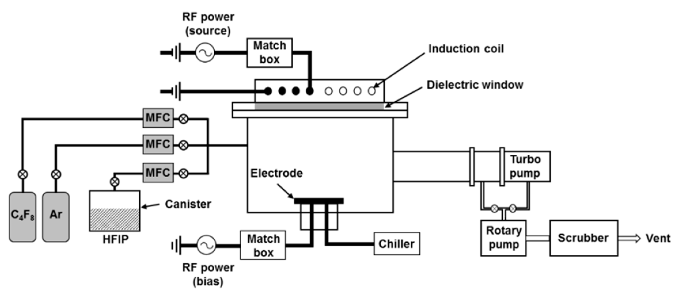
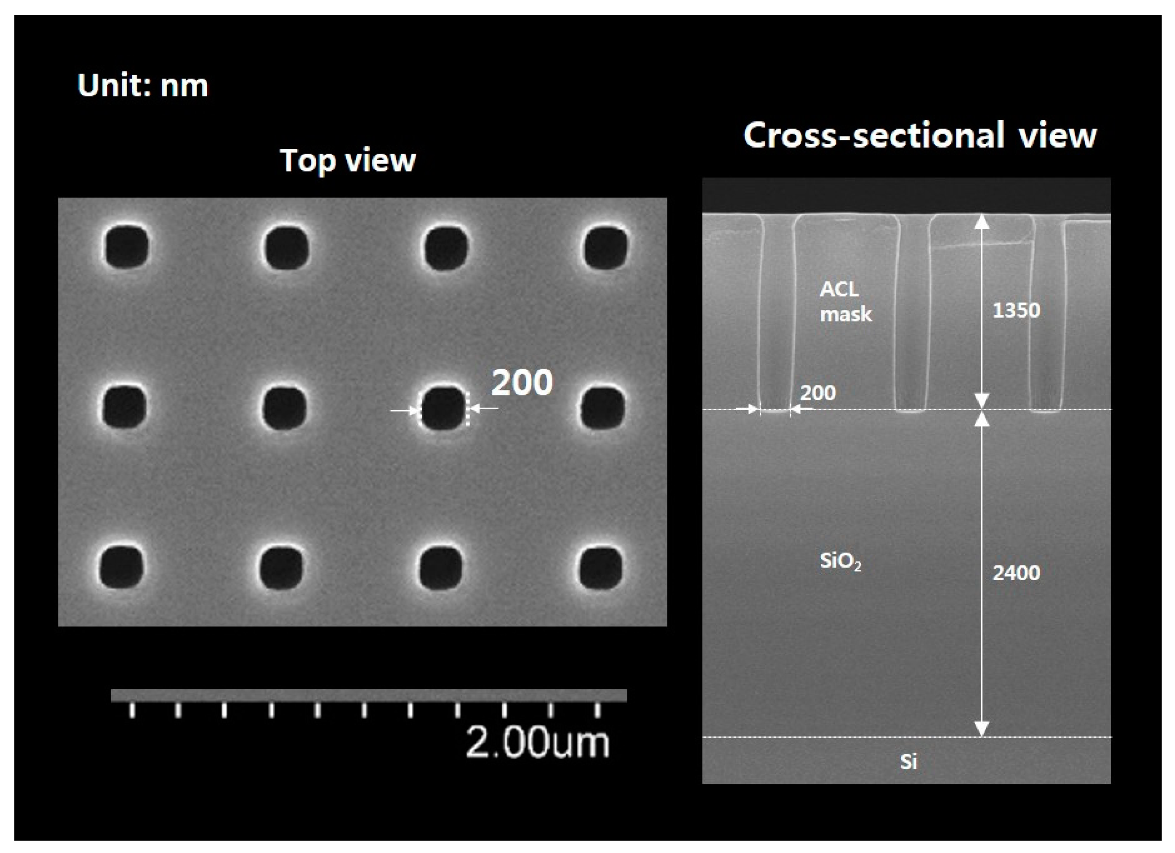
In this work, hexafluoroisopropanol (HFIP) was examined for the plasma etching of SiO2, and its etch features were compared with those in C4F8. HFIP is partially fluorinated alcohol, whose GWP is ~190, which is notably lower compared with those of PFCs. The etching features of SiO2 were explored by varying the bias voltage. The thickness of the steady-state fluorocarbon film piled on the surface of the substrate and the optical emission intensity of fluorine radicals were investigated to explain the etch characteristics. The etching of a SiO2 contact hole with a diameter of 200 nm and an aspect ratio of 12 was also conducted in each plasma.
3. Results and Discussion
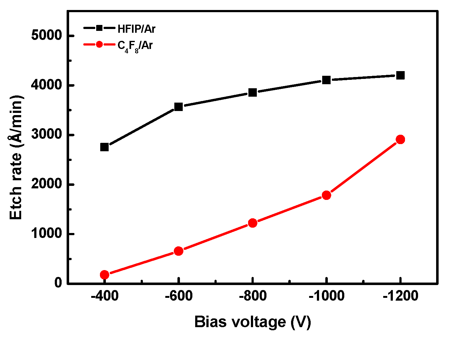
Figure 3 shows the SiO
2 etch rates in HFIP/Ar and C
4F
8/Ar plasmas as a function of the bias voltage. The etch rates in both HFIP/Ar and C
4F
8/Ar plasmas monotonically increased with the magnitude of the bias voltage. This behavior is a typical characteristic of plasma etching because the energy of the incident ions bombarding the substrate increases with the magnitude of the bias voltage. The SiO
2 etch rates in the HFIP/Ar plasma were faster compared with those in the C
4F
8/Ar plasma under all etching conditions.
Higher etch rates in HFIP/Ar plasmas compared with in C4F8/Ar plasmas can be attributed to the different chemistry of the discharge materials. HFIP contains oxygen atoms, while C4F8 does not contain them, meaning that oxygen radicals are only formed in the HFIP/Ar plasma. A thin fluorocarbon film (a so-called steady-state fluorocarbon film) is subject to being piled on the surface of the substrate during etching in fluorocarbon-containing plasmas, such as HFIP and C4F8.
Oxygen radicals react with the fluorocarbon films into volatile reaction products, such as CO, CO2 and COF2. Therefore, the steady-state fluorocarbon films on the surface of SiO2 would be thinner in the HFIP/Ar plasma compared with in the C4F8/plasma. Since fluorocarbon films act as etch resistance against radicals and ions during etching, SiO2 is more vulnerable to the etching reaction in the HFIP/Ar plasma compared with in the C4F8/plasma. Therefore, the SiO2 etch rates in HFIP/Ar plasmas were faster compared with those in C4F8/Ar plasmas.
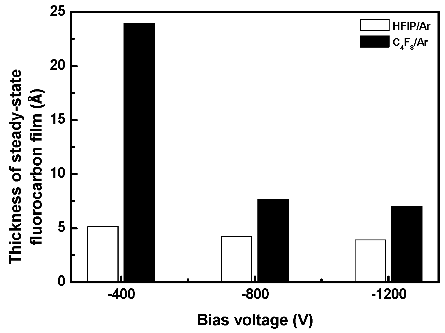
The characteristics of the steady-state fluorocarbon films in each plasma were analyzed to support this explanation.
Figure 4 shows the thickness of the steady-state films piled on the SiO
2 surfaces at bias voltages of −400, −800 and −1200 V in HFIP/Ar and C
4F
8/Ar plasmas, respectively. The thickness of the steady-state fluorocarbon film piled on the SiO
2 surface was obtained using the silicon 2p X-ray photoelectron spectra before and after etching [
14]. The thickness of the fluorocarbon film (d) is expressed as
where
I and
I0 are the intensities of the Si 2p peak in the presence and absence of the fluorocarbon film, respectively. λ is the inelastic mean free path of Si 2p electrons in the fluorocarbon film and assumed to be 2.5 nm [
14]. ϕ is the angle of electron emission with respect to the surface normal, and it was 45° in this study.
The film thickness decreased with increasing the magnitude of the bias voltage in both HFIP/Ar and C4F8/Ar plasmas. The thickness of the steady-state fluorocarbon film in the HFIP/Ar plasma was lower than that in the C4F8/Ar plasma at all bias voltages. As mentioned above, the fluorocarbon film piled on the surface of the substrate acts as an etch resistance during etching in fluorocarbon-containing plasmas, meaning that as the thickness of the steady-state film on the surface of the substrate decreases, the substrate is more vulnerable to the etching reaction. Thus, the SiO2 etch rates were faster in the HFIP/Ar plasma.
Figure 4 also shows that the difference in the thicknesses of the steady-state fluorocarbon films between HFIP/Ar and C
4F
8/Ar plasmas decreased with the increase in the magnitude of the bias voltage. This behavior is similar to the difference in the SiO
2 etch rates between the two plasmas (see
Figure 3). It was 2580 Å/min at a bias voltage of −400 V, monotonically decreased with the increasing magnitude of the bias voltage and was 1300 Å/min at a bias voltage of −1200 V. Therefore, we concluded that the thickness of the steady-state fluorocarbon film piled on the surface of SiO
2 directly affects the etch rate of SiO
2 in HFIP/Ar and C
4F
8/Ar plasmas.
One can argue why the SiO
2 etch rates in the C
4F
8/Ar plasma increased more rapidly with the magnitude of the bias voltage compared with those in the HFIP/Ar plasma. This can be attributed to the difference in the C-F bond energy between HFIP and C
4F
8. C
4F
8 comprises carbons forming a cyclic ring, and the C-F bond energy in C
4F
8 is 4.4 eV [
15]. Comparatively, carbons are linearly connected in HFIP, and the C-F bond in the linear carbons is usually stronger than that in the cyclic carbons.
For example, the bond energies of C-F in CF
4, C
2F
6 and C
3F
8 are 5.6, 5.4 and 5.3 eV, respectively [
16]. The C-F bond energy in HFIP is expected to be similar to that in C
3F
8 since HFIP consists of three linearly-located carbons although they are not exactly the same [
17]. As the bias voltage increases, the dissociation of C-F bonds is subject to increase in both HFIP and C
4F
8.
Since the C-F bond energy in C4F8 is lower than that in HFIP, the dissociation of C-F bonds occurs more vigorously in C4F8 than in HFIP, thereby, resulting in a higher increase in the formation of fluorine radicals (which are responsible for SiO2 etching by producing volatile reaction products, such as SiFx and COF2) in C4F8/Ar plasmas compared with in HFIP/Ar plasmas. Thus, the SiO2 etch rates increased more rapidly with the magnitude of the bias voltage in the C4F8/Ar plasma compared with those in the HFIP/Ar plasma.
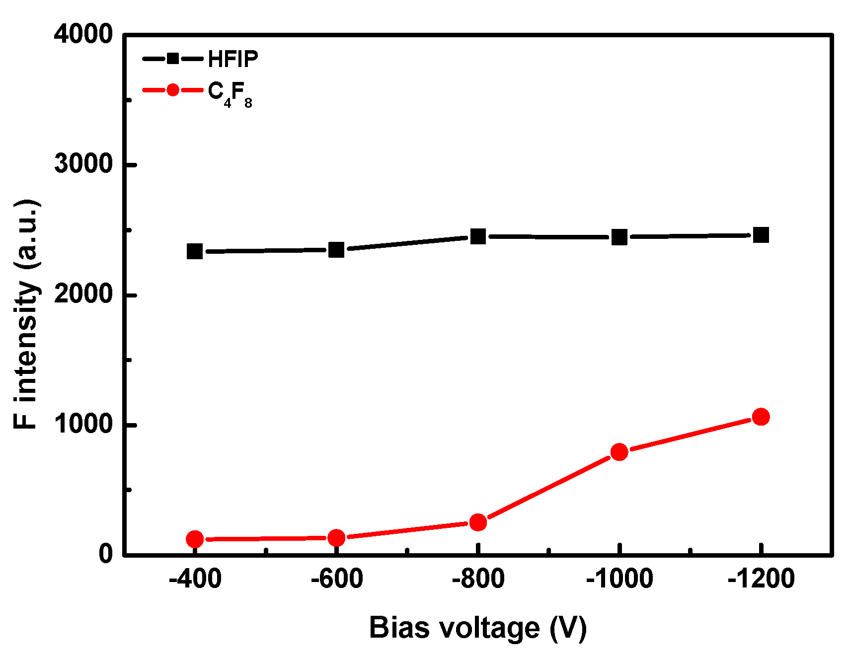
A higher increase in the production of fluorine radicals when increasing the magnitude of the bias voltage in C
4F
8/Ar plasmas compared with in HFIP/Ar plasmas was investigated using OES.
Figure 5 shows the optical emission intensities of the fluorine radicals generated in HFIP/Ar and C
4F
8/Ar plasmas, respectively, as a function of the bias voltage. Fluorine radicals were identified as lines at 685.6 and 703.7 nm [
18].
The fluorine-radical intensities in the HFIP/Ar plasma were greater compared with those in the C4F8/Ar plasma. As the magnitude of the bias voltage increased, the intensity of fluorine radicals increased slightly in the HFIP/Ar plasma and increased rapidly in the C4F8/Ar plasma. Therefore, the OES measurements support the higher increase in the SiO2 etch rates with the magnitude of the bias voltage in the C4F8/Ar plasma compared with those in the HFIP/Ar plasma.
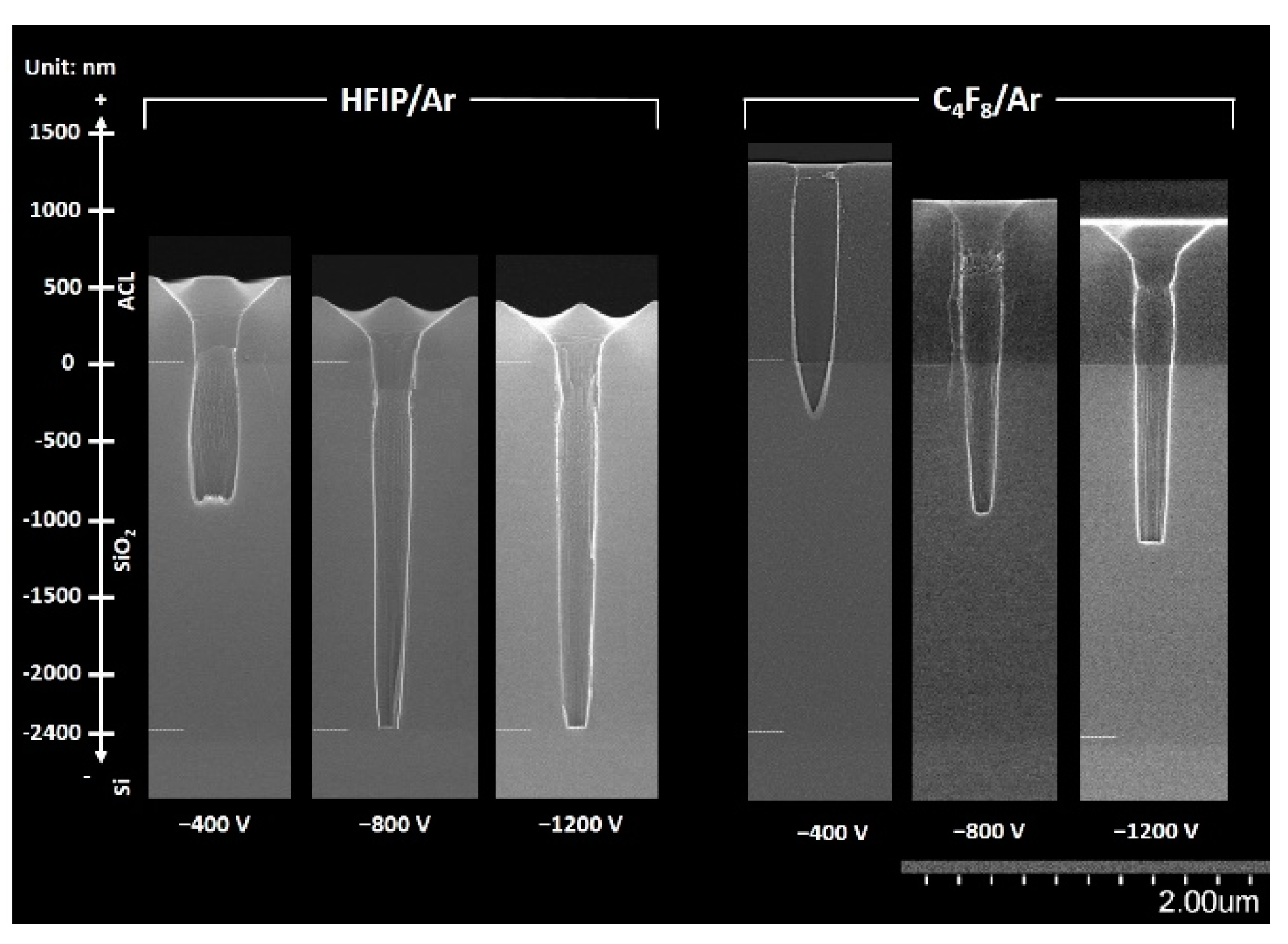
Figure 6 shows the SEM images of the 200 nm diameter SiO
2 contact holes etched in HFIP/Ar and C
4F
8/Ar plasmas at various bias voltages. The SEM images were taken after the fluorocarbon films were removed by ashing. For SEM measurements, the samples were coated with Pt for 20 s. In all cases, etching was done for 12 min. As expected, the etch depth of the SiO
2 contact hole increased with the magnitude of the bias voltage in both HFIP/Ar and C
4F
8/Ar plasmas.
Furthermore, the etch depths of the contact hole in the HFIP/Ar plasma were greater compared with those in the C
4F
8/Ar plasma at all bias voltages. This agrees with the results from higher SiO
2 etch rates in HFIP/Ar plasmas compared with those in C
4F
8/Ar plasmas (see
Figure 3). At bias voltages higher than −800 V, SiO
2 contact holes with an aspect ratio of 12 were completely etched in the HFIP/Ar plasma.
Comparatively, even at the highest magnitude of the bias voltage (−1200 V) used in this study, SiO2 contact holes were not etched through in the C4F8/Ar plasma. In the HFIP/Ar plasma, sidewall necking below the top of the hole was improved by increasing the magnitude of the bias voltage, and fairly anisotropic SiO2 contact hole etching was successfully achieved at a bias voltage of −1200 V. Finally, the use of HFIP (whose GWP is significantly lower than that of PFC) for the plasma etching of SiO2 contact holes was realized.
4. Conclusions
HFIP was examined for the plasma etching of SiO2, and its etch characteristics were compared with those in C4F8. The SiO2 etch rates in the HFIP/Ar plasma were faster compared with those in the C4F8/Ar plasma under all etching conditions used in this study. This was attributed to oxygen atoms in HFIP, which produced oxygen radicals. Since oxygen radicals react with the fluorocarbon film piled up on the surface of the substrate into volatile products, the steady-state fluorocarbon films on the surface of SiO2 were thinner and more vulnerable to the etching reaction (a correspondingly higher SiO2 etch rate) in the HFIP/Ar plasma compared with in the C4F8/Ar plasma.
XPS analysis confirmed that the thicknesses of the steady-state fluorocarbon films piled on the surface of SiO2 in the HFIP/Ar plasma were lower compared with those in C4F8/Ar plasma. The etch rates in both HFIP/Ar and C4F8/Ar plasmas monotonically increased with the magnitude of the bias voltage. However, due to the higher dissociation of the C-F bonds in CF4 compared with in HFIP, the SiO2 etch rates in the C4F8/Ar plasma increased more rapidly with the magnitude of the bias voltage than did those in the HFIP/Ar plasma.
The etch profiles of the 200 nm diameter SiO2 contact holes showed that the etch depths of the hole in the HFIP/Ar plasma were deeper compared with those in the C4F8/Ar plasma at all bias voltages, thus, agreeing with the results from the higher SiO2 etch rates in HFIP/Ar plasmas compared with those in C4F8/Ar plasmas. In the HFIP/Ar plasma, the 200 nm diameter SiO2 contact holes with an aspect ratio of 12 were completely etched at bias voltages greater than −800 V, and fairly anisotropic SiO2 contact hole etching was achieved successfully at a bias voltage of −1200 V. Finally, this study realized the use of HFIP (whose GWP is significantly lower than that of PFC) for the plasma etching of SiO2 contact holes.


