Abstract
Hydrogen-nitrogen hybrid passivation treatment for growing high-property gate oxide films by high-temperature wet oxidation, with short-time NO POA, is proposed and demonstrated. Secondary ion mass spectroscopy (SIMS) measurements show that the proposed method causes hydrogen and appropriate nitrogen atoms to accumulate in Gaussian-like distributions near the SiO2/SiC interface. Moreover, the hydrogen atoms are also incorporated into the grown SiO2 layer, with a concentration of approximately 1 × 1019 cm−3. The conductance characteristics indicate that the induced hydrogen and nitrogen passivation atoms near the interface can effectively reduce the density of interface traps and near-interface traps. The current-voltage (I-V), X-ray photoelectron spectroscopy (XPS), and time-dependent bias stress (TDBS) with ultraviolet light (UVL) irradiation results demonstrate that the grown SiO2 film with the incorporated hydrogen passivation atoms can effectively reduce the density of oxide electron traps, leading to the barrier height being improved and the leakage current being reduced.
1. Introduction
The 4H polytype of silicon carbide (4H-SiC) has attractive potential as a semiconductor suitable for power device applications, due to its superior material performance. Among the wide-bandgap semiconductor materials, one of the unique characteristics of 4H-SiC is that stable silicon dioxide (SiO2) films, as gate dielectrics, can be directly formed by thermal oxidation, which provides the opportunity to manufacture 4H-SiC metal-oxide-semiconductor field-effect transistors (MOSFETs) using conventional silicon technology. As a result, 4H-SiC MOSFETs received widespread attention due to the commercial demand for efficient power conversion and control.
Even though 4H-SiC MOSFETs are already commercially available, there are still some problems that need to be further solved; some of these problems include, for example, the low channel mobility, and poor oxide reliability and threshold voltage shift (Vth) under gate-bias stressing, which may due to the high density of charge traps near the SiO2/SiC interface and the low quality of gate oxide [1,2,3,4]. In the recent years, the introduction of various impurity elements, by annealing treatments after dry oxidation, have been widely examined to improve the SiO2/SiC interface quality of 4H-SiC MOSFETs [5,6,7,8]. Although NO post-oxidation annealing (POA) may be the most commonly used passivation technique for 4H-SiC MOSFET devices, recent research has suggested that NO annealing at high temperatures, for a long duration, will introduce excess nitrogen near the SiO2/SiC interface, which can induce additional deep energy-level hole traps and even cause a negative shift in threshold voltage [9,10,11]. Thus, it is necessary to optimize the long-duration nitrogen treatment, in order to avoid excess nitrogen passivation atoms reducing the density of hole traps induced in the 4H-SiC MOS devices.
On the other hand, it has been reported that thermal oxidation in wet ambience with H2O gas results in the improvement of 4H-SiC MOS interface quality [12,13,14,15,16,17,18]. Several previous works showed that the channel mobility of 4H-SiC MOSFETs on a-face, C-face, and Si-face can be significantly enhanced by wet oxidation [12,13,14]. The work reported by Hirai et al. showed that wet H2O oxidation treatment significantly reduced the intrinsic strain of gate oxide near the interface, compared to dry O2 oxidation [17], which may be due to the ability of H2O to remove the carbon-related byproducts of oxidation from the interface more efficiently than O2 [16]. However, it is worth noting that the previous research on 4H-SiC wet oxidation was mostly performed at an environment temperature less than or equal to 1200 °C [12,13,14,15,16,17,18], which may be limited by the maximum operating temperature of the quartz furnace. Although the former researchers have reported the influence of wet oxidation on the channel mobility of 4H-SiC MOSFETs [12,13,14], the information about the effect of high-temperature wet oxidation on the integrity of gate oxide is not sufficient. Meanwhile, recent studies of 4H-SiC high-temperature dry oxidation suggest that higher oxidation temperatures (>1200 °C) can effectively improve the performance of 4H-SiC MOSFETs [19,20,21,22,23]. Therefore, the influence of high-temperature wet oxidation on 4H-SiC is worth studying, and, in particular, the effect mechanism of high-temperature wet oxidation on the properties of the grown oxide should be further investigated.
In this work, pyrogenic wet oxidation in high-temperature ambience of 1300 °C, with short-time NO POA, was used to grow gate oxide films on n-type 4H-SiC. As a reference, MOS capacitors were also fabricated by dry O2 oxidation with Ar POA, using the same processes conditions. The gate oxide characteristics and effect mechanisms of different oxidation treatments are investigated by capacitance-voltage (C-V), parallel conductance-voltage (G-V), conductance-frequency (G-f), current-voltage, time-dependent bias stress with ultraviolet light irradiation, secondary ion mass spectroscopy, and X-ray photoelectron spectroscopy measurements. The corresponding phenomena are discussed in depth.
2. Experimental Methods
Si-face 4° off-axis 4H-SiC substrates with 5-μm-thick n-type epitaxial layer of 1 × 1016 cm−3 doping concentration were used in this experiment. Following the Radio Corporation of America cleaning, hydrofluoric acid dipping and water rinsing, this wafer was employed to fabricate two kinds of samples. A set of samples were oxidized in pyrogenic wet ambience at 1300 °C for 18 min. Afterwards, NO POA was performed under the condition of 1175 °C for 15 min (denoted as H&N hybrid passivation). Additionally, the contrast samples were only oxidized in dry O2 ambience at 1300 °C for 30 min, then annealed in Ar ambience at 1175 °C for 2 h (denoted as Ar passivation). The thicknesses of gate oxide were obtained by spectroscopic ellipsometry, which were 60 nm and 50 nm for the H&N hybrid and Ar passivation samples, respectively. At last, MOS capacitor was fabricated by evaporating nickel at the backside to form ohmic contact and sputtering aluminum on the oxide surface for the gate electrode.
In this study, Keysight B1505A analyzer (Keysight Technologies, Penang, Malaysia) with CASCADE probe station was employed to measure the electrical characteristics of the samples. The capacitance-voltage, parallel conductance-voltage and accumulation conductance-frequency were measured to evaluate SiO2/SiC interface qualities. The conductance method was employed to extract the densities of interface states (Dit). Forward current-voltage curves were characterized at room temperature to estimate the gate oxide integrity (GOI). Time-dependent bias stress measurements with UVL irradiation (λ = 365 nm) were applied to induce the trapping and releasing charges. Secondary ion mass spectroscopy measurements were performed in Evans Analytical Group (EAG) laboratories to determine the density of hydrogen and nitrogen, and the relative contents of silicon, oxygen and carbon. X-ray photoelectron spectroscopy, using Thermo Fisher ESCALAB Xi+ surface analysis equipment (Thermo Fisher Scientific, London, United Kingdom), was used to investigate the grown SiO2 bandgap and the energy band alignments of SiO2/SiC structures.
3. Results and Discussion
3.1. Nitrogen and Hydrogen Distribution
Secondary ion mass spectroscopy was used in EAG laboratories to determine the distribution of hydrogen and nitrogen in the SiO2/SiC structure, as well as the relative content of Si, O, and C near the SiO2/SiC interface, as shown in Figure 1. It is clear that no nitrogen is observed above the detection limit in the Ar passivation sample, and the H atoms observed in the Ar passivation sample probably come from the H in the 4H-SiC epilayer, which are redistributed during the high-temperature dry oxidation process [24,25]. For the H&N hybrid passivation sample, although it was only annealed in NO ambience at 1175 °C for 15 min, it is clearly observed that the short-time NO POA creates a Gaussian-like profile of nitrogen, with a peak of 4.5 × 1020 cm−3 at the SiO2/SiC interface only, which is much lower than that reported in ref. [11], indicating that the nitrogen-associated hole traps are optimized. Moreover, it is found that the hydrogen concentration distributed uniformly in the grown SiO2 film, which is about 1 × 1019 cm−3 and Gaussian-like accumulation with a peak of 1.8 × 1020 cm−3 near the SiO2/SiC interface (red line in Figure 1a), which are bigger concentrations than that distributed in the Ar passivation sample. Given that the wet ambience generated by the pyrogenic method is a H2O and O2 mixture gas (O2-rich wet ambience), the additional hydrogen atoms in the H&N hybrid passivation sample must be introduced by high-temperature wet oxidation, which may terminate the dangling bonds and exhibit an effect on trap passivation. Thus, it is considered that high-temperature wet oxidation not only increases the oxidation rate, reducing the intrinsic strain, but also introduces additional hydrogen passivation atoms into the SiO2/SiC structure, especially into the grown SiO2 layer, which may help to improve the quality of the gate oxide.

Figure 1.
SIMS profiles for the (a) H&N hybrid and (b) Ar passivation samples.
3.2. Interface Characteristics
In order to investigate the improvements in the rapid hydrogen-nitrogen hybrid passivation method for the SiO2/SiC interface, the capacitance-voltage, parallel conductance-voltage, and accumulation conductance-frequency measurements were employed at room temperature in the dark. Additionally, the conductance method was used to determine the density of interface states. The H&N hybrid passivation samples show a positive drift in the first measured C-V curves, compared with the reference Ar passivation samples, as shown in Figure 2a. It is inferred that negative fixed charges are induced into the grown SiO2 by H&N hybrid passivation, which may generate by the additional incorporated H atoms in the gate oxide [26]. Further, compared to the Ar passivation samples, the conductance peak of the H&N hybrid passivation samples is much lower, which is related to the energy loss caused by the interface traps capture and release the majority carriers [27]. Thus, it is considered that the proposed hydrogen–nitrogen hybrid passivation method can significantly improve the quality of the SiO2/SiC interface.
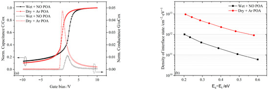
Figure 2.
(a) C-V and G-V curves measured at 10 kHz for the fresh point and (b) Dit extract by conductance method for the both samples.
Figure 2b shows the energy distributions of Dit below the conduction band edge of SiC for both the samples, which are extracted by the conductance method [23]. It is clear that the density of interface states for the H&N hybrid passivation samples is about one order of magnitude lower than that of the Ar passivation samples, which is consistent with the trend of the conductance peak in the G-V curves. The results showed that the proposed method can effectively reduce the density of interface states with 1 × 10¹² to 6 × 1010 cm−2eV−1 below the conduction band edge of SiC.
Figure 3 shows the results of the accumulation conductance-frequency measurements for both the samples, which were obtained by sweeping from 1 kHz to 1 MHz with a gate oxide electric field of 1.5 MV/cm (accumulation states). It is clear that in all the samples, the accumulation conductance increases linearly in logarithmic coordinates of the measurement frequency, indicating that the closer to the SiO2/SiC interface, the greater the density of near-interface traps [28]. Importantly, the accumulation conductance of the H&N hybrid passivation sample exhibits 10 times smaller compared to the reference Ar passivation sample, and this trend is consistent with the change in Dit below the conduction band edge of SiC (shown in Figure 2b). It is considered that the reduction in Dit and near-interface traps in the H&N hybrid passivation sample may be ascribed to hydrogen and nitrogen atoms accumulated near the interface, to terminate the dangling bonds of the Si and/or C atoms and relax the interfacial strain.
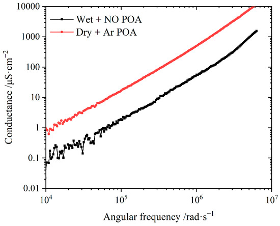
Figure 3.
Conductance-frequency curves measured at accumulation state for the both samples.
3.3. Gate Oxide Integrity
The forward I-V measurements for the fresh points at room temperature were applied to determine the gate oxide integrity for both the samples, and the extracted current density-electric field (J-E) characteristics are shown in Figure 4. Compared with the Ar passivation samples, the H&N hybrid passivation treatment with a faster oxidation rate does not degrade the GOI, and the first measured current densities of the H&N hybrid passivation samples are even smaller, especially when the electric field strength is lower than 3 MV/cm. It is considered that the small current peaks in the first measured curves, under low electric field strength, may relate to the near-interface traps, which can be effectively reduced by H&N hybrid passivation. When the field strength is over 6 MV/cm, the Fowler-Nordheim (F-N) tunneling current is clearly observed in all the samples. The conduction band barrier height between the SiC epilayer and grown SiO2 film can be derived from the linear fit of measured ln(J/E2) versus 1/E using the Lenzlinger-Snow (LS) equation [29], which are 2.61 eV and 2.42 eV for the H&N hybrid and Ar passivation samples, respectively. The results show that the gate oxide integrity can be effectively improved by the proposed hydrogen-nitrogen hybrid passivation, leading to the leakage current being reduced.
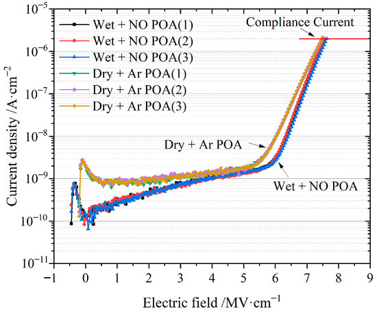
Figure 4.
First measured current density-electric field characteristics for both the samples.
3.4. X-Ray Photoelectron Spectroscopy Measurements
In order to gather more information about the energy band alignments, XPS measurements were also applied to the difference samples in this work. The O 1s energy loss spectra of the grown SiO2 film for both the samples are shown in Figure 5a, and the bandgap of SiO2 is extracted using the onsets of energy loss [30,31]. The valence band spectra of the SiC epilayer and grown SiO2 film for the different samples are shown in Figure 5b,c, in which the valence band offset is obtained by identifying the maximum difference between the valence band of SiO2 and SiC [31]. Given that the bandgap of 4H-SiC is 3.26 eV, the conduction band offset between the SiC epilayer and grown SiO2 film can be calculated by the method in ref. [31].

Figure 5.
(a) O 1s energy loss spectra for both the samples Valence band spectra for the (b) H&N hybrid and (c) Ar passivation samples.
Figure 6 shows the energy band alignments determined by XPS measurements and forward I-V measurements (listed in brackets), in which the conduction band barrier heights extracted by F-N tunneling current fitting are both lower than that estimated by XPS measurements. The reason for this may be that the gate leakage current includes not only the F-N tunneling of electrons from the accumulated 4H-SiC epilayer, but also the Poole-Frenkel emission of electrons from the interfacial traps located at an energy level of 2.48 eV, below the SiO2 conduction band [32]. The work reported by Samanta et al. reviewed this issue, and prescribed a more accurate formula to estimate the oxide field and F-N current expression [32,33]. In this paper, the forward I-V data are measured at room temperature, so the effect on the extracted conduction band barrier height is small and the contrast trends for the different samples are credible. Compared with the Ar passivation samples, the SiO2 bandgap grown with high-temperature wet oxidation treatment is much bigger, resulting in the conduction band offset being larger for the H&N hybrid passivation sample. Additionally, the results are consistent with the trend of conduction band barrier height extracted by F-N tunneling current fitting. Thus, the energy band alignments show that the SiO2 grown using high-temperature wet oxidation with short-time NO POA is much closer to the ideal value, indicating that the proposed hydrogen-nitrogen hybrid treatment can improve the quality of gate oxide.
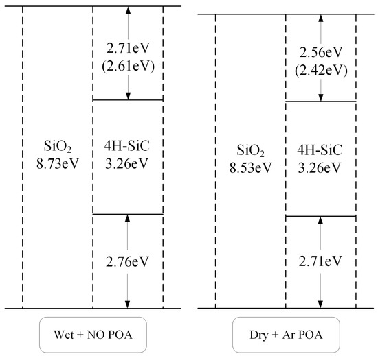
Figure 6.
Energy band alignments of the SiO2/SiC structures for the different samples.
3.5. Time-Dependent Bias Stress Measurements with UVL Irradiation
It has been reported, by A. Lelis et al., that TDBS measurements can be employed to characterize the oxide traps in SiO2/SiC MOS structures [3]. Therefore, in this work, the C-V characteristics were measured before and after TDBS with UVL irradiation, in order to estimate the negative and positive charge density, as shown in Figure 7a,b. The initial C-V curves (black line) were measured on the fresh points. Successively, the second C-V curves (red line) were measured after bias stress of 2 MV/cm for 600 s in the dark. Subsequently, the third C-V curves (green line) were measured after 600 s of bias stress of −2 MV/cm with UVL irradiation. At last, the fourth curves (blue line) were measured after the same bias stress condition as the second curves. Compared with the first curves, without suffering from bias stress, it is clearly found that the positive shift in flat band voltage (Vfb) in the second curves is much larger for the Ar passivation sample, indicating that more electrons are captured by the oxide traps during positive bias stress. Moreover, the density of oxide electron traps can be extracted by (Cox/qS)·|∆Vfb|, in which |∆Vfb| is the shifts of Vfb, relative to the initial curve (shown in Figure 8). Besides, in the third curves, Vfb shows a large negative shift after the negative bias stress with UVL irradiation, which cannot return back to the position of the second curves, even after the same positive bias stress condition in the fourth curves, especially for the H&N hybrid passivation samples. It is inferred that the proposed method, with short-time NO POA, induces some slow-state hole traps, which can be extracted by the method in ref. [34] (also shown in Figure 8).
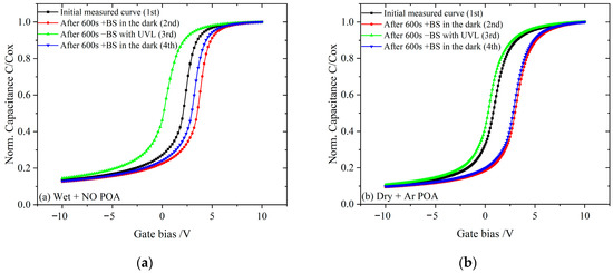
Figure 7.
Typical C-V characteristics measured at 10 kHz in the dark before and after positive and negative time-dependent bias stress (BS) with UVL irradiation for the (a) H&N hybrid and (b) Ar passivation samples.
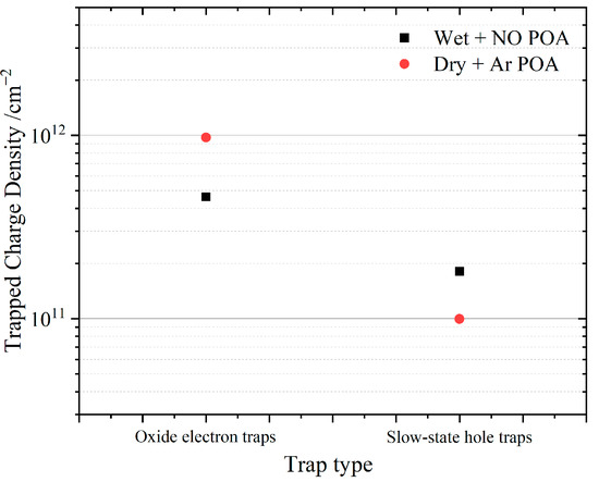
Figure 8.
Extracted oxide electron traps and slow-state hole traps for both the samples.
The oxide electron traps and slow-state hole traps extracted by TDBS measurements with UVL irradiation are shown in Figure 8. Compared with the Ar passivation samples, it is obvious that the H&N hybrid passivation treatment yields a reduction of more than half in the oxide electron traps, as well as increases the slow-state hole traps nearly two-fold. Thus, it is considered that the proposed method, with 15 min of NO POA, is an optimized nitrogen treatment, which introduces appropriate nitrogen passivation atoms that accumulate near the SiO2/SiC interface, with a peak of 4.5 × 1020 cm−3 (shown in Figure 1a). On the one hand, the incorporated additional H and appropriate N passivation atoms can effectively reduce the oxide electron traps and improve the reliability of the gate oxide, which is exactly consistent with the conclusion obtained from the above I-V and XPS characteristics. On the other hand, the appropriate nitrogen passivation atoms near the SiO2/SiC interface can avoid inducing large numbers of slow-state hole traps, leading to tolerance to the stability of device characteristics.
4. Conclusions
An efficient hydrogen-nitrogen hybrid passivation treatment for improving the quality of the SiO2/SiC interface and gate oxide films, by conducting 18 min of high-temperature wet oxidation and 15 min of NO POA, is proposed. In order to demonstrate and contrast N-type 4H-SiC MOS capacitors with H&N hybrid and Ar passivation, they have been fabricated and tested. For the H&N hybrid passivation samples, SIMS results reveal that hydrogen and nitrogen atoms create Gaussian-like profile distributions near the SiO2/SiC interface. Further, the additional hydrogen passivation atoms are also incorporated into the grown SiO2 layer during the high-temperature wet oxidation process. Compared with the Ar passivation samples, the analysis of conductance data showed that the density of interface traps and near-interface traps can be reduced by about one order of magnitude by the H&N hybrid passivation treatment, which induced hydrogen and nitrogen passivation atoms near the SiO2/SiC interface. Moreover, the XPS, I-V and TDBS with UVL irradiation results indicate that the proposed wet oxidation process with NO POA can also improve the integrity of the gate oxide. It is found that the SiO2 film grown with hydrogen passivation atoms incorporated can reduce the density of oxide electron traps by more than half, resulting in the conduction band barrier height being improved and the gate leakage current being reduced. However, the proposed method, with 15 min of NO POA, also inevitably induces some slow-state hole traps in the grown SiO2. This work demonstrates that high-temperature wet oxidation with short-time NO POA is promising for the rapid fabrication of high-quality SiO2 films on the 4H-SiC epilayer.
Author Contributions
Conceptualization, Y.J.; methodology, Y.J.; software, S.S.; validation, X.L., Q.L. and S.W.; formal analysis, Y.G.; investigation, Y.J.; resources, X.T. and Y.Z.; data curation, Y.J.; writing—original draft preparation, Y.J.; writing—review and editing, Y.J. and Y.G.; visualization, K.Q.; supervision, H.C.; project administration, H.C.; funding acquisition, Y.J., X.L. and Y.G. All authors have read and agreed to the published version of the manuscript.
Funding
This work was jointly supported by National Natural Science Foundation of China (No. 62104192), Natural Science Basic Research Program of Shaanxi Province (No. 2021JQ-717) and the Scientific Research Program Funded by Shaanxi Provincial Education Department (No. 20JK0909 and NO. 21JK0919).
Institutional Review Board Statement
Not applicable.
Informed Consent Statement
Not applicable.
Data Availability Statement
Not applicable.
Conflicts of Interest
The authors declare no conflict of interest.
References
- Liu, G.; Tuttle, B.R.; Dhar, S. Silicon carbide: A unique platform for metal-oxide-semiconductor physics. Appl. Phys. Rev. 2015, 2, 021307. [Google Scholar] [CrossRef]
- Kimoto, T. Material science and device physics in SiC technology for high-voltage power devices. Jpn. J. Appl. Phys. 2015, 54, 040103. [Google Scholar] [CrossRef]
- Lelis, A.J.; Green, R.; Habersat, D.B.; Ei, M. Basic mechanisms of threshold-voltage instability and implications for reliability testing of SiC MOSFETs. IEEE Trans. Electron. Devices 2015, 62, 316–323. [Google Scholar] [CrossRef]
- Green, R.; Lelis, A.; Habersat, D. Threshold-voltage bias-temperature instability in commercially-available SiC MOSFETs. Jpn. J. Appl. Phys. 2016, 55, 04EA03. [Google Scholar] [CrossRef]
- Sharma, Y.K.; Ahyi, A.C.; Isaacs-Smith, T.; Modic, A.; Park, M.; Xu, Y.; Garfunkel, E.L.; Dhar, S.; Feldman, L.C.; Williams, J.R. High-mobility stable 4H-SiC MOSFETs using a thin PSG interfacial passivation layer. IEEE Electron Device Lett. 2013, 34, 175–177. [Google Scholar] [CrossRef]
- Liu, G.; Ahyi, A.C.; Xu, Y.; Isaacs-Smith, T.; Sharma, Y.K.; Williams, J.R.; Dhar, S. Enhanced inversion mobility on 4H-SiC using phosphorus and nitrogen interface passivation. IEEE Electron Device Lett. 2013, 34, 181–183. [Google Scholar] [CrossRef]
- Rong, H.; Sharma, Y.K.; Dai, T.; Li, F.; Jennings, M.R.; Russell, S.A.; Martin, D.M.; Mawby, P.A. High temperature nitridation of 4H-SiC MOSFETs. Mater. Sci. Forum 2016, 858, 623–626. [Google Scholar] [CrossRef]
- Hirai, H.; Kita, K. Low temperature wet-O2 annealing process for enhancement of inversion channel mobility and suppression of Vfb instability on 4H-SiC (0001) Si-face. Appl. Phys. Lett. 2018, 113, 172103. [Google Scholar] [CrossRef]
- Rozen, J.; Dhar, S.; Dixit, S.K.; Afanas’ev, V.V.; Roberts, F.O.; Dang, H.L.; Wang, S.; Pantelides, S.T.; Williams, J.R.; Feldman, L.C. Increase in oxide hole trap density associated with nitrogen incorporation at the SiO2/SiC interface. J. Appl. Phys. 2008, 103, 124513. [Google Scholar] [CrossRef]
- Rozen, J.; Dhar, S.; Zvanut, M.E.; Williams, J.R.; Feldman, L.C. Density of interface states, electron traps, and hole traps as a function of the nitrogen density in SiO2 on SiC. J. Appl. Phys. 2009, 105, 658–664. [Google Scholar] [CrossRef]
- Jia, Y.; Lv, H.; Tang, X.; Han, C.; Song, Q.; Zhang, Y.; Zhang, Y.; Dimitrijev, S.; Han, J.; Haasmann, D. Influence of various NO annealing conditions on N-type and P-type 4H-SiC MOS capacitors. J. Mater. Sci. Mater. Electron. 2019, 30, 10302–10310. [Google Scholar] [CrossRef]
- Senzaki, J.; Kojima, K.; Harada, S.; Kosugi, R.; Suzuki, S.; Suzuki, T.; Fukuda, K. Excellent effects of hydrogen postoxidation annealing on inversion channel mobility of 4H-SiC MOSFET fabricated on (11–20) face. IEEE Electron Device Lett. 2002, 23, 13–15. [Google Scholar] [CrossRef]
- Fukuda, K.; Kato, M.; Kojima, K.; Senzaki, J. Effect of gate oxidation method on electrical properties of metal-oxide-semiconductor field-effect transistors fabricated on 4H-SiC C(000-1) face. Appl. Phys. Lett. 2004, 84, 2088–2090. [Google Scholar] [CrossRef]
- Okamotoa, M.; Tanaka, M.; Yatsuo, T.; Fukuda, K. Effect of the oxidation process on the electrical characteristics of 4H-SiC p-channel metal-oxide-semiconductor field-effect transistors. Appl. Phys. Lett. 2006, 89, 023502. [Google Scholar] [CrossRef]
- Palmieri, R.; Radtke, C.; Boudinov, H.; Silva, E.F. Improvement of SiO2/4H-SiC interface properties by oxidation using hydrogen peroxide. Appl. Phys. Lett. 2009, 95, 713. [Google Scholar] [CrossRef]
- Hirohisa, H.; Koji, K. Suppression of byproduct generation at 4H-SiC/SiO2 interface by the control of oxidation conditions characterized by infrared spectroscopy. Appl. Phys. Express 2015, 8, 021401. [Google Scholar] [CrossRef]
- Hirohisa, H.; Koji, K. Difference of near-interface strain in SiO2 between thermal oxides grown on 4H-SiC by dry-O2 oxidation and H2O oxidation characterized by infrared spectroscopy. Appl. Phys. Lett. 2017, 110, 956. [Google Scholar] [CrossRef]
- Indari, E.D.; Yamashita, Y.; Hasunuma, R.; Oji, H.; Yamabe, K. Relationship between electrical properties and interface structures of SiO2/4H-SiC prepared by dry and wet oxidation. AIP Adv. 2019, 9, 105018. [Google Scholar] [CrossRef] [Green Version]
- Richard, H.K.; Koji, K. Fabrication of SiO2/4H-SiC (0001) interface with nearly ideal capacitance-voltage characteristics by thermal oxidation. Appl. Phys. Lett. 2014, 105, 032106. [Google Scholar] [CrossRef] [Green Version]
- Harsh, N.; Chow, T.P. 4H-SiC MOS capacitors and MOSFET fabrication with gate oxidation at 1400 °C. Mater. Sci. Forum 2014, 778, 607–610. [Google Scholar] [CrossRef]
- Thomas, S.M.; Sharma, Y.K.; Crouch, M.A.; Fisher, C.A.; Perez-Tomas, A.; Jennings, M.R.; Mawby, P.A. Enhanced field effect mobility on 4H-SiC by oxidation at 1500 °C. IEEE J. Electron Devices Soc. 2014, 2, 114–117. [Google Scholar] [CrossRef]
- Hosoi, T.; Nagai, D.; Sometani, M.; Katsu, Y.; Takeda, H.; Shimura, T.; Takei, M.; Watanabe, H. Ultrahigh-temperature rapid thermal oxidation of 4H-SiC(0001) surfaces and oxidation temperature dependence of SiO2/SiC interface properties. Appl. Phys. Lett. 2016, 109, 182114. [Google Scholar] [CrossRef]
- Jia, Y.; Lv, H.; Song, Q.; Tang, X.; Xiao, L.; Wang, L.; Tang, G.; Zhang, Y.; Zhang, Y. Influence of oxidation temperature on the interfacial properties of n-type 4H-SiC MOS capacitors. Appl. Surf. Sci. 2016, 397, 175–182. [Google Scholar] [CrossRef] [Green Version]
- Suzuki, S.; Fukuda, K.; Okushi, H.; Nagai, K.; Sekigawa, T.; Yoshida, S.; Tanaka, T.; Kazuo, A. Effect of post-oxidation-annealing in hydrogen on SiO2/4H-SiC interface. Mater. Sci. Forum 2000, 338, 1073–1076. [Google Scholar] [CrossRef]
- Zhu, Q.; Qin, F.; Li, W.; Wang, D. Improvement of SiO2/4H-SiC interface properties by electron cyclotron resonance microwave nitrogen-hydrogen mixed plasma post-oxidation annealing. Appl. Phys. Lett. 2013, 103, 461–463. [Google Scholar] [CrossRef]
- Kamiya, K.; Ebihara, Y.; Chokawa, K.; Kato, S.; Shiraishi, K. Origins of negative fixed charge in wet oxidation for SiC. Mater. Sci. Forum 2013, 742, 409–412. [Google Scholar] [CrossRef]
- Palmieri, R.; Radtke, C.; Silva, M.R.; Boudinov, H.; Silva, E.F. Trapping of majority carriers in SiO2/4H-SiC structures. J. Phys. D Appl. Phys. 2009, 42, 125301. [Google Scholar] [CrossRef]
- Haasmann, D.; Dimitrijev, S. Energy position of the active near-interface traps in metal-oxide-semiconductor field-effect transistors on 4H-SiC. Appl. Phys. Lett. 2013, 103, 113506. [Google Scholar] [CrossRef] [Green Version]
- Lenzlinger, M.; Snow, E.H. Fowler-Nordheim tunneling into thermally grown SiO2. J. Appl. Phys. 1969, 40, 278–283. [Google Scholar] [CrossRef]
- Yu, H.Y.; Li, M.F.; Cho, B.J.; Yeo, C.C.; Joo, M.S. Energy gap and band alignment for (HfO2)x(Al2O3)1−x on (100) Si. Appl. Phys. Lett. 2002, 81, 376–378. [Google Scholar] [CrossRef] [Green Version]
- Hosoi, T.; Kirino, T.; Mitani, S.; Nakano, Y.; Nakamura, T.; Shimura, T.; Watanabe, H. Relationship between interface property and energy band alignment of thermally grown SiO2 on 4H-SiC (0001). Curr. Appl. Phys. 2012, 12, S79–S82. [Google Scholar] [CrossRef]
- Samanta, P.; Mandal, K.C. Leakage current conduction, hole injection, and time-dependent dielectric breakdown of n-4H-SiC MOS capacitors during positive bias temperature stress. J. Appl. Phys. 2017, 121, 034501. [Google Scholar] [CrossRef]
- Samanta, P. Mechanistic analysis of temperature-dependent current conduction through thin tunnel oxide in n+-polySi/SiO2/n+-Si structures. J. Appl. Phys. 2017, 122, 094502. [Google Scholar] [CrossRef]
- Jia, Y.; Lv, H.; Tang, X.; Song, Q.; Zhang, Y.; Zhang, Y.; Dimitrijev, S.; Han, J. Comparative study on slow-state near interface hole traps in NO and Ar annealed N-type 4H-SiC MOS capacitors by ultraviolet light. J. Mater. Sci. Mater. Electron. 2018, 29, 14292–14299. [Google Scholar] [CrossRef]
Publisher’s Note: MDPI stays neutral with regard to jurisdictional claims in published maps and institutional affiliations. |
© 2021 by the authors. Licensee MDPI, Basel, Switzerland. This article is an open access article distributed under the terms and conditions of the Creative Commons Attribution (CC BY) license (https://creativecommons.org/licenses/by/4.0/).