Article

Study the Passivation Characteristics of Microwave Annealing Applied to APALD Deposited Al2O3 Thin Film

1
Institute of Microelectronics, Department of Electrical Engineering, National Cheng Kung University, Tainan 70101, Taiwan
2
Department of Mechanical Engineering, Southern Taiwan University of Science and Technology, Tainan 71005, Taiwan
*
Author to whom correspondence should be addressed.
Coatings 2021, 11(12), 1450; https://doi.org/10.3390/coatings11121450
Submission received: 27 October 2021 / Revised: 19 November 2021 / Accepted: 23 November 2021 / Published: 25 November 2021

Abstract

:
In this study, a self-developed atmospheric pressure atomic layer deposition (APALD) system is used to deposit Al2O3 passivation film, along with the use of precursor combinations of Al(CH3)3/H2O to improve its passivation characteristics through a short-time microwave post-annealing process. Comparing the unannealed and microwave-annealed samples whose temperature is controlled at 200–500 °C, APALD non-vacuum deposited film can be realized with a higher film deposition rate, which is beneficial for increasing the production throughput while at the same time reducing the operating cost of vacuum equipment at hand. Since the microwave has a greater penetration depth during the process, the resultant thermal energy provided can be spread out evenly to the entire wafer, thereby achieving the effect of rapid annealing. The film thickness is subsequently analyzed by TEM, whereas the chemical composition is verified by EDS and XPS. The negative fixed charge and interface trap density are analyzed by the C-V measurement method. Finally, the three major indicators of τeff, SRV, and IVoc are analyzed by QSSPC to duly verify the excellent passivation performance.

1. Introduction

At present, mainstream solar cells are predominantly represented by the so-called passivation of the emitter and rear contact (PERC) solar cells. PERC solar cells are among the typical solar cells with high efficiency [1,2,3]. Among them, the most distinctive feature goes to the implementation of the back passivation layer structure, which is used to effectively weaken the problematic role of the dangling bonds over the back of the silicon wafer, thereby mitigating the unwanted surface recombination-induced defects [4,5]. Aluminum oxide (Al2O3) is a high-k material with a wide energy gap (~9 eV). The structural properties of the Si/Al2O3 interface have been carefully studied through a series of surface analysis methods. It was found that Al2O3 could provide excellent Si surface passivation for photovoltaic applications [6]. The silicon oxide (SiOx) layer formed at the interface may play a key role in the origin of the negative fixed charge, which can reduce the surface recombination rate. However, it is still necessary to obtain a sound grasp of the passivation mechanism of the interfacial SiOx layer on the silicon surface [7,8].
There are many techniques for depositing Al2O3 thin films, such as common plasma-assisted chemical vapor deposition (PECVD) [9,10], atmospheric pressure chemical vapor deposition (APCVD) [11], sputtering technology [12,13], the sol–gel process [14], pulsed laser deposition [15], and atomic layer deposition (ALD) [16,17]. Using ALD to deposit Al2O3 film has many advantages. Its Al2O3 film and the underlying silicon substrate have good thermal and chemical stability, and can achieve a high-quality Si/Al2O3 interface [18].
Among them, the atmospheric pressure atomic layer deposition (APALD) process independently developed by our research group is different from the traditional vacuum equipment. It has a better film deposition rate, potentially leading to an increase in the production rate. It can achieve the required production capacity through stacking process cycles. The space-divided array nozzle module system is used to develop APALD; that is, the reactant feed is no longer alternately sent to a reaction chamber, but the reaction chamber is divided into multiple different sections. These reaction sections are separated by an internal air curtain, and the air shield also acts as a compartment between the reaction sections to prevent cross-reaction and parasitic precipitation on the reaction chamber wall [19,20]. The very design improves the deposition reaction and the speed of the precursors purging, thereby greatly improving the deposition efficiency without losing the usual advantages of ALD [21]. The common precursors for depositing Al2O3 films using ALD are trimethylaluminum (TMA) and H2O, both of which are volatile liquids, thus they are easy to control and inexpensive in the process [22].
The study found that the Al2O3 film deposited using H2O as a precursor would grow a very thin SiOx interface layer on the Si/Al2O3 interface after the post-deposition annealing processes. Passivation occupies an extremely important position. The interface layer increases the negative fixed oxide charge and reduces the interface trap density [18]. The annealing process ensued after film deposition can help to reorganize the Si/Al2O3 interface. There are many annealing processes, such as furnace annealing [18], rapid thermal annealing (RTA) [23], and microwave annealing [23,24]. The way that microwave annealing provides energy is quite different from the other traditional annealing methods. A typical traditional heating procedure is conducted by external radiation, which is in direct contrast with microwaves that penetrate the material in the form of electromagnetic waves. Energy can be obtained both inside and outside of the material. Uniformity-wise, therefore, microwave annealing is adopted in this study. In this instance, microwave energy could comfortably penetrate the multilayer film structure to provide the thermal energy necessary for delivering uniform heating and annealing. [24] The special mechanism involved in microwave heating delivers the effect of significantly reducing the annealing temperature and holding time. On the other hand, since the degree of microwave absorption depends on the rotation of the material’s dipole, microwave annealing can be used to selectively heat the material. It is a potential way to improve energy usage efficiency.
In this study, the self-developed APALD equipment is used to deposit Al2O3 thin films that act as passivation films for PERC solar cells. The ALD reactions use TMA and water vapor as precursors. With the microwave post-annealing process, the power control is used to maintain a temperature between 200–500 °C, to ensure excellent performance can be achieved by a very short microwave annealing temperature holding time. Furthermore, through a series of studies, the influence of microwave energy level on the performance of the passivation layer deposited on silicon wafers is probed and the changes in the electrical and structural properties of the Si/Al2O3 interface as affected by microwave induction are compared. Finally, the effective minority carrier lifetime (τeff) and component trap density analysis are used to verify the characteristics of the Al2O3 passivation film with or without microwave annealing and with different annealing powers administered.

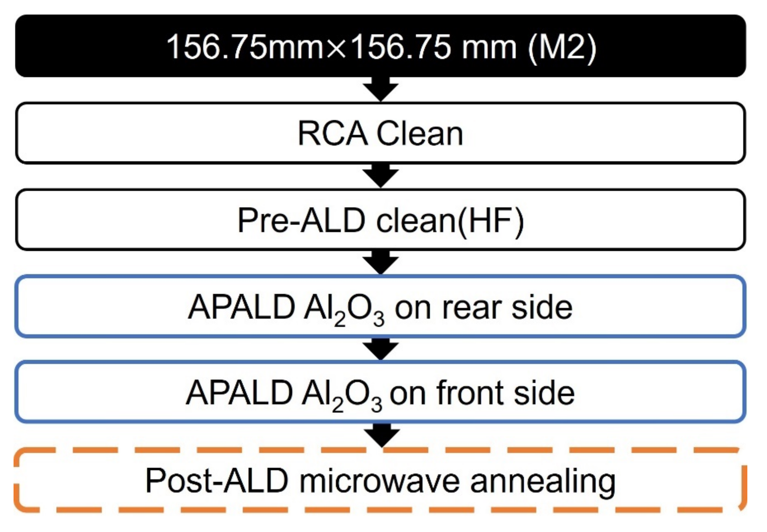
2. Materials and Methods

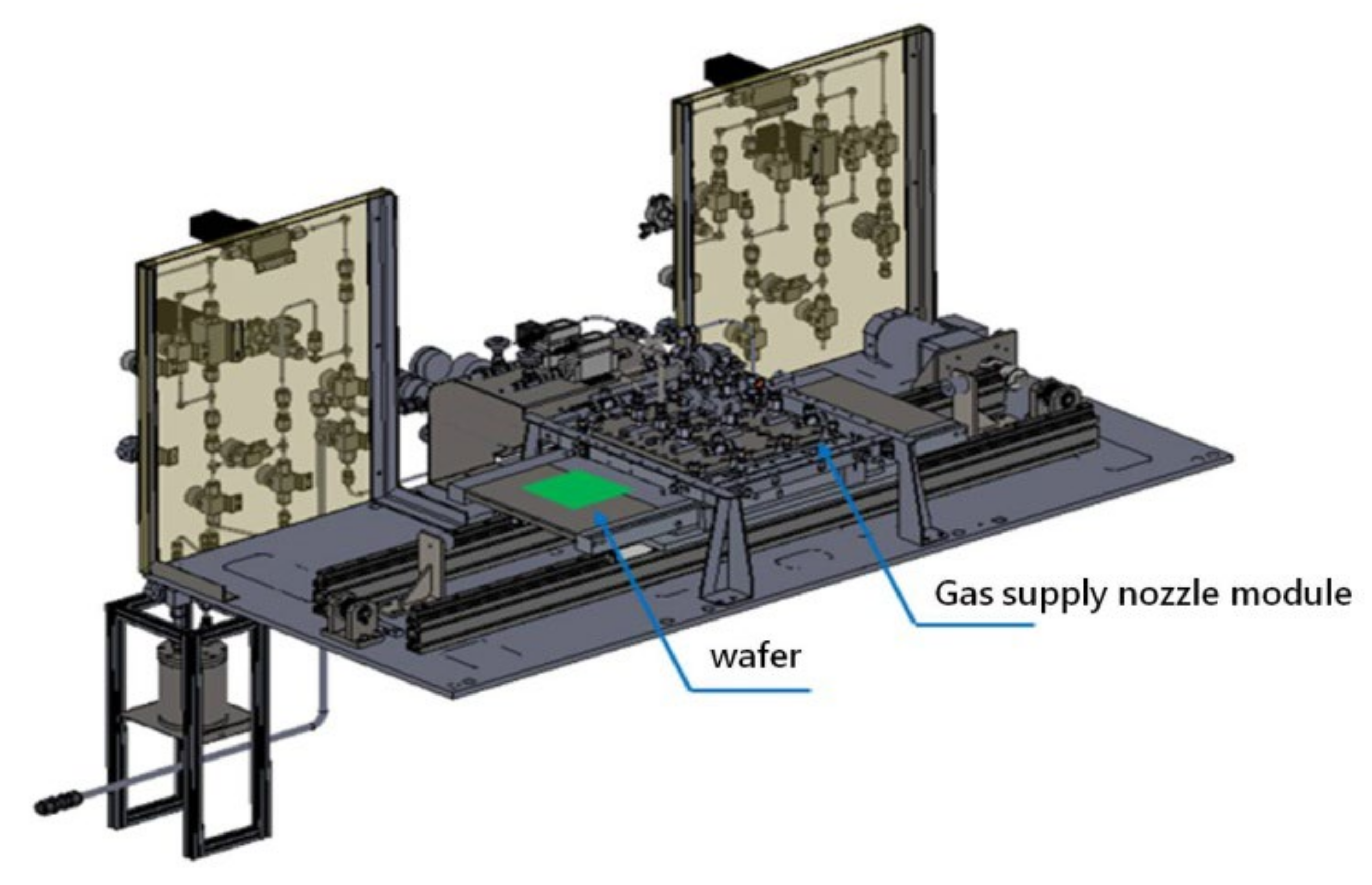
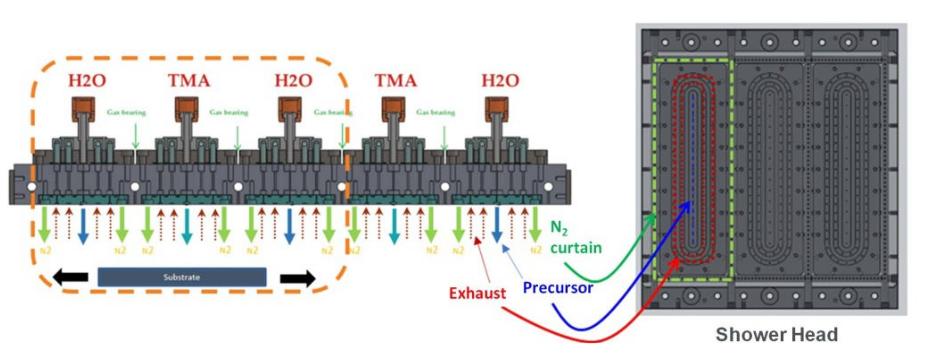
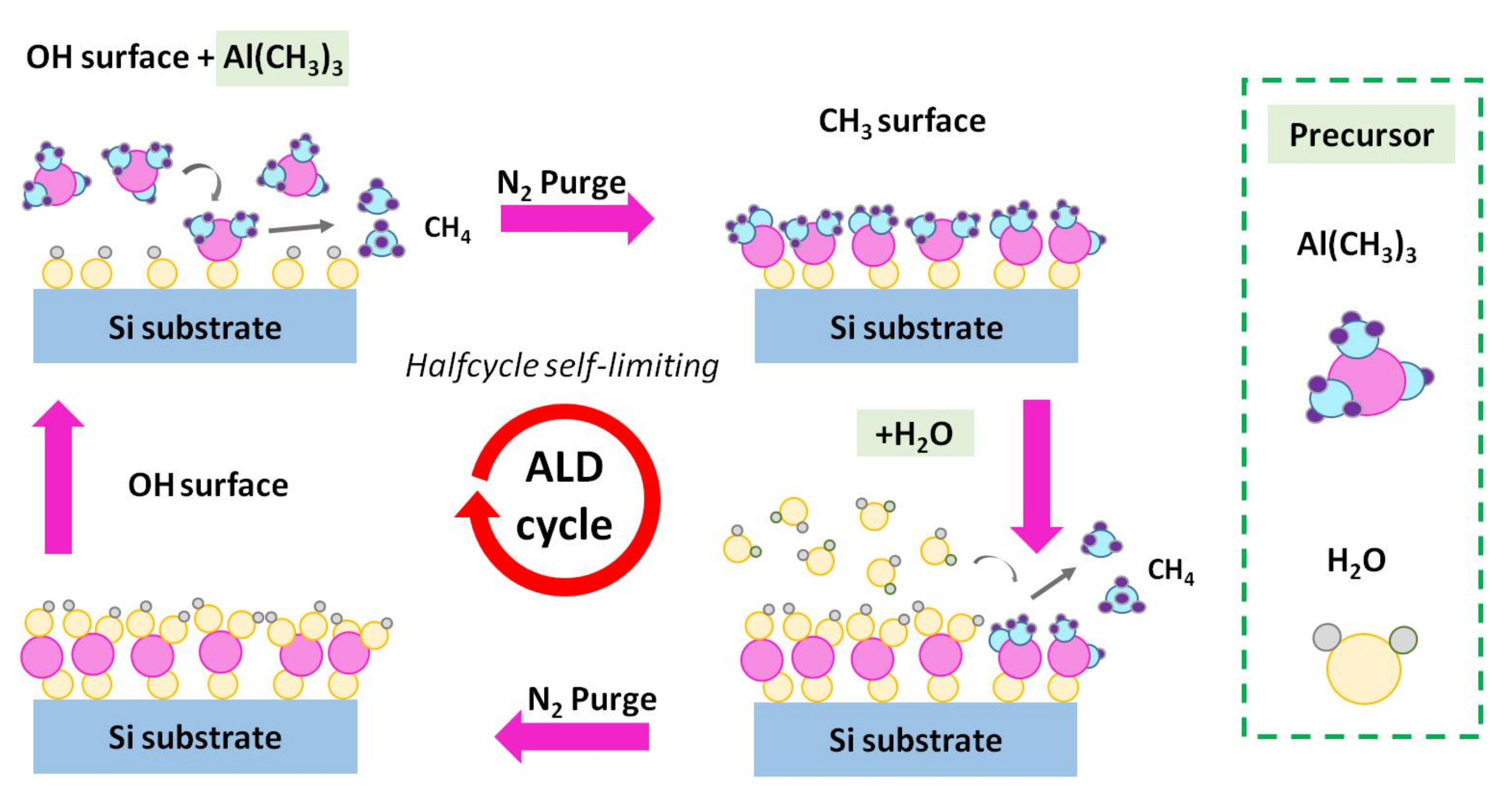
2.1. Al2O3 Film Growth via APALD of TMA and H2O

The silicon wafer Si (100) substrate is a P-type wafer grown by the Czochralski (CZ) method, with a resistivity value of 1–10 Ω-cm, a thickness of 475 μm, and a size of 156.75 mm × 156.75 mm (M2). The substrate is thoroughly cleaned before the subsequent film deposition to narrow down the scope of process variables that might play a role in impacting the performance of the devices. First, the surface of the silicon wafer is cleaned by the RCA (Radio Corporation of America, New York, NY, USA) cleaning process and with unwanted native oxides removed by a diluted hydrofluoric acid solution before placing it in the chamber. In this study, 50% hydrofluoric acid and deionized water were mixed at a ratio of 20:1, and the silicon substrate was immersed in the solution for 2 min, followed by rinsing the silicon substrate with rapid deionized water and then drying the surface of the substrate with nitrogen.
The experimental flow of the thin film deposition pursued in this study is shown in Figure 1 below. The effective minority carrier lifetime measurement is conducted using a double-sided Al2O3 film structure. After the substrate is cleaned, Al2O3 films are deposited over the front and back of the silicon wafer as the passivation layer of the PERC solar cell. The APALD, which is the equipment independently developed and manufactured by our research team, is schematically shown in Figure 2. Note that the APALD process is different from traditional vacuum ALD equipment, in the sense that it has a higher film deposition rate, which potentially can increase the production rate and reduce the cost of vacuum equipment investment. For current manufacturers, it is easy to replace the production line equipment with one of high throughput to increase the production capacity of solar cells [19,21].
The key design of the self-developed APALD equipment is the introduction of a spatial matrix nozzle module design. The working principle of the matrix gas nozzle module can be elucidated pictorially as shown in Figure 3. The Al2O3 film is deposited on the substrate that has concurrently undergone the back and forth movement. Once the saturated reaction is completed over the substrate surface, the by-products and excess precursors are then blown away with inert gas. The matrix gas shower is designed to separate the precursor from the inert gas, and the reaction is divided into multiple different areas. The inert gas forms a gas curtain between TMA and H2O. The gas curtain can prevent the reaction zones from reacting with each other. If the film cannot be deposited smoothly or pollution has ever occurred, the air extraction system is used to purify the pipeline to ensure the film quality and surface morphology. The space matrix design renders the gas deliveries more uniform after the TMA and H2O precursors enter the reaction chamber, and at the same time, the interactions can be avoided among the precursors to form dust, which would affect the film quality and film uniformity [20].
Figure 4 below shows the complete cycle of the deposition of the aluminum oxide film using the atomic layer deposition system. The hydroxyl bonds (Si–OH) are formed on the surface of the substrate, and the first precursor TMA (Al(CH3)3) is introduced. The surface OH groups react to produce CH4 molecules, and the introduced TMA will not react with each other due to the self-limiting effect, nor will it cause physical adsorption on the substrate. After the reaction of TMA with the OH groups on the surface is completed, an inert gas is introduced to take away the excess TMA and the by-product CH4 produced after the reaction. Next, the second precursor, water vapor (H2O), reacts with Si–O–Al(HO)2 to facilitate the adjacent Al–O bonding. Since the water molecules also undergo self-limited reactions, inert gas is introduced to flush away the CH4 by-product and excess water molecules after the reaction, thereby completing an ALD cycle to generate an atomic film. The number of continuous cycles can be specified to control the thickness of the aluminum oxide film.
Al2O3 coatings were deposited under TMA/H2O exposures, as described by Equations (1) and (2) [22].
AlOH + Al(CH3)3 → AlOAl(CH3)2 + CH4
AlCH3 + H2O → AlOH + CH4
The Al2O3 film uses TMA and H2O as precursors in the APALD process. The APALD process parameters implemented to plate the Al2O3 film is shown in Table 1. After 110 ALD cycles, the Al2O3 film with a thickness of about 10 nm is deposited. The Al2O3 film is selected as the passivation film because it has a high charge density and can deliver passivation with excellent conformity over the surface of the P-type wafer. It is currently widely used as a back passivation material for the mass production of PERC cells. Chemical passivation and field-effect passivation are the two main approaches for the passivation of aluminum oxide films. The field-effect passivation produced by Al2O3 is related to the fixed charges (Qf) in the Al2O3 layer, and the negative fixed charge results in band bending. The chemical passivation produced by Al2O3 can reduce the dangling bonds on the wafer surface and this, in turn, can reduce the occurrence of surface recombination, thereby prolonging the minority carrier lifetime [25].

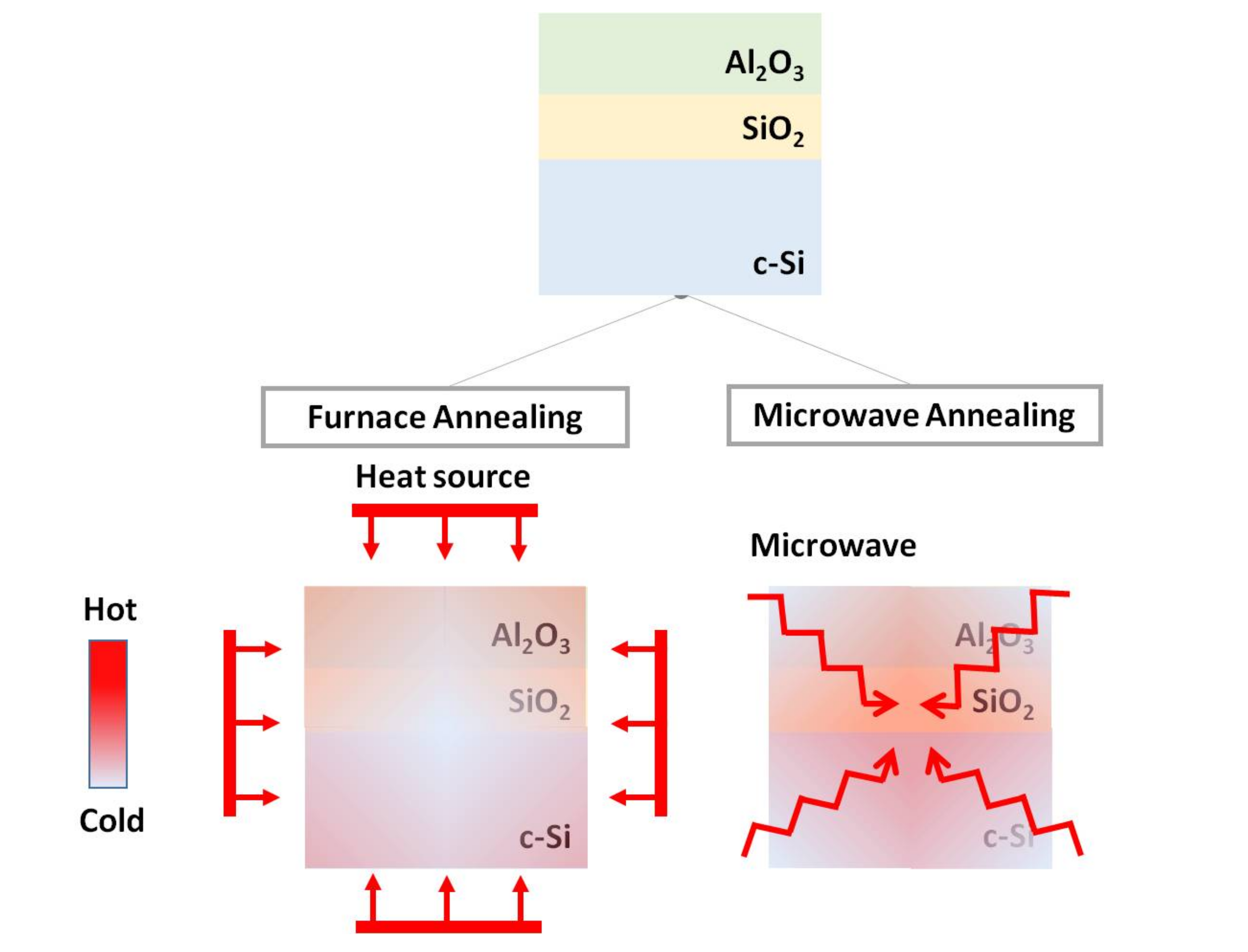
2.2. Microwave Annealing Process

The post-annealing process can improve the passivation effect, and obtain better film quality through the addition of thermal energy. The traditional annealing process can achieve good results through high temperature and long-term annealing. Figure 5 schematically compares traditional annealing with microwave annealing in terms of differences in the mechanism. Since traditional thermal conduction provides heat energy with a thermal gradient into the film, the temperature of the inner part of the film is relatively low, and it takes a longer time to achieve energy transfer.
Microwave annealing, on the other hand, behaves in the exact opposite manner. The energy penetrates in a form of an electromagnetic wave to the internal part of the film, thereby ensuring the entire film would receive microwave energy uniformly so that better annealing efficiency is achieved [26,27]. However, the microwave has non-thermal effects to be dealt with. It is found from the literature that the activation energy required in the microwave process is less than that of a general heating process, which in turn leads to the recombination process that occurs at a lower temperature [28,29].
In this study, the passivation annealing process was performed by adjusting the microwave power which would translate to different process temperatures. The relevant process parameters are shown in Table 2 for the subsequent discussion on the structural properties and electrical characteristics of the Si/Al2O3 interface. A 2.45 GHz microwave sintering furnace (pyro 260, Milestone, Sorisole, Italy) is exploited for annealing operations. This equipment is characterized by rapid heating capability and a rotating diffuser. By distributing the microwave energy uniformly in the entire chamber, the standing wave effect can be minimized to ensure an entire chamber is basked in a uniform temperature. During the annealing process, the sample is placed at a height of 5 cm in the middle of the chamber, where the distribution of the electromagnetic field is the most uniform. The temperature of the sample is measured using an infrared pyrometer to read the temperature. The power varies from 150 to 800 W, the corresponding temperature is 200–500 °C, and the annealing time is held for 5 min.
The field emission transmission electron microscope (FE-TEM, JEM-2100F, JEOL, Tokyo, Japan) was used to observe the Si/Al2O3 interface. In principle, the electromagnetic lens is used to focus and accelerate the electrons, so that the electrons colliding with the atoms of the material would veer their directions, resulting in a combination of transmitted and elastically scattered electron beams. The electron beams are then amplified and focused by an electromagnetic lens to form a final image, whereas an energy-dispersive X-ray spectrometry (EDS) is used for chemical composition analysis. At 200 kV, its point-to-point resolution in TEM mode is ≤0.19 nm. The capacitance-voltage (C-V) measurement was carried out using the Keithly 4200 system (Solon, OH, USA). The C-V sample using an Al point electrode of 90 μm in diameter patterned on the Al2O3 film was prepared with thermal evaporation equipment. The C-V experiment was conducted with a bias voltage ranging from −3 to +3 V to obtain 50 mV ac-coupled signals at 1, 100, and 1000 kHz. Utilizing the standard planar capacitor equation, the dielectric constant of alumina was calculated based on the accumulated capacitance value with the accuracy estimated to be ±5%.
The Silicon Wafer Lifetime Tester (WCT-120, Sinton Consulting Inc., Boulder, CO, USA) operating with the quasi-steady-state photoconductance (QSSPC) mode was used to assess the minority carrier lifetime and implied open-circuit voltage. The very information obtained can be used in turn to estimate the effective surface recombination velocity (SRV). The surface chemical analysis was performed with a PHI 5000 VersaProbe (ULVAC-PHI, Inc., Chigasaki, Japan) XPS system with a micro-focused Al Kα X-ray and the take-off angle of the photoelectron set at 45°. A dual-beam charge neutralizer was used for charge compensation. The X-ray and acceptance lens of the analyzer were rasterized over a sample area of 500 µm × 500 µm.

3. Results and Discussion

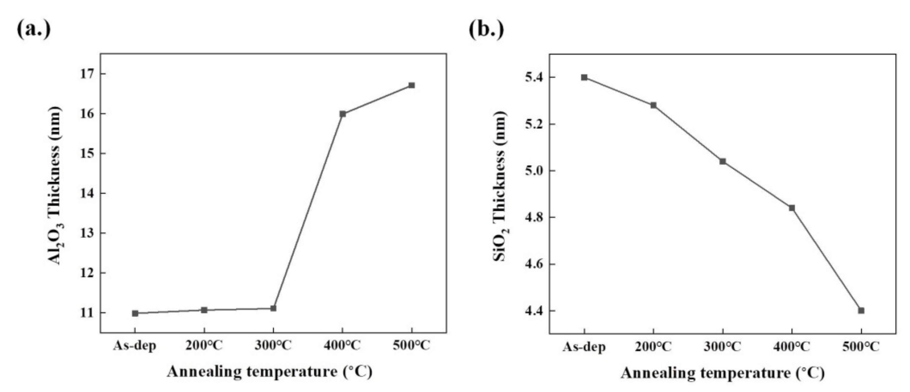
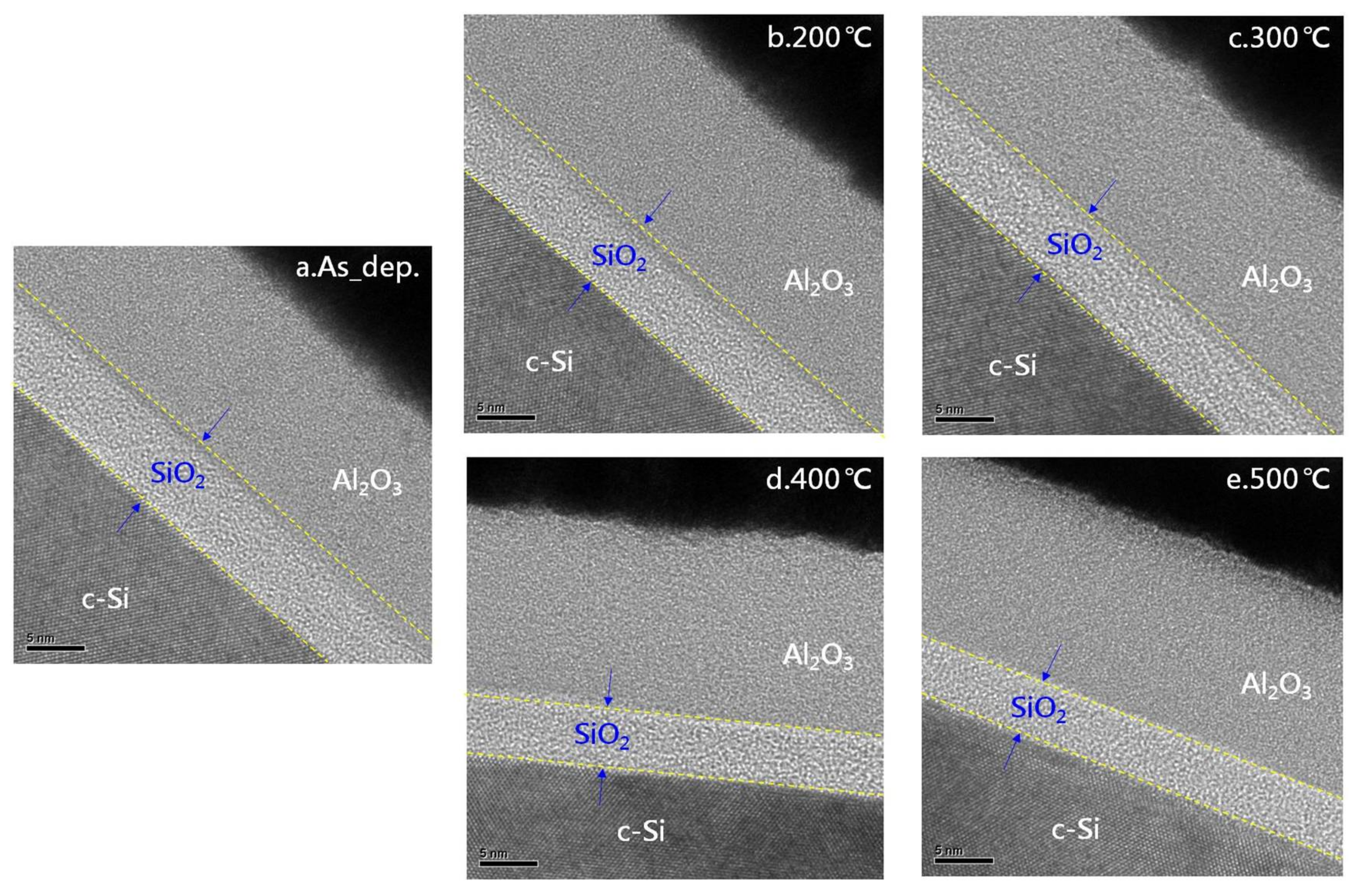
3.1. Transmission Electron Microscope (TEM) Image

First of all, the structural characteristics of the Si/Al2O3 interface under the influences of different annealing conditions were evaluated through the field emission transmission electron microscope (FE-TEM, JEM-2100F, JEOL, Tokyo, Japan). Figure 6a–e depict several FE-TEM images of Al2O3 deposited on a silicon substrate which reveal the details of the Si/Al2O3 interface in the pristine condition and also after the microwave annealing treatment conducted at a temperature ranging from 200–500 °C. The resultant thickness variations of the Al2O3 and the SiO2 layers at the Si/Al2O3 interface are presented in Figure 7 for comparison. As observed in Figure 6, an extremely thin SiO2 layer between Si and Al2O3 play an important role in passivating Al2O3. When investigated in detail, the SiO2 surface reveals a slight change in appearance. Further analysis and discussion follow, conducted through EDS.
Figure 7a shows that the unannealed Al2O3 film thickness is around 10.99 nm after APALD deposition, and the film becomes thicker when increasing the annealing temperature. The film thickening is not apparent initially at the temperature of 200 and 300 °C, and the respective thicknesses are found to be 11.07 and 11.11 nm. However, as the temperature exceeds 400 °C, the thickness noticeably rises to 15.99 nm, and the trend then levels off at 500 °C with a thickness of 16.71 nm. This phenomenon is ascribed to the additional energy provided by the microwave field to diffuse the Al, and as the microwave energy increases, the Al diffusion at the Si/Al2O3 interface is accentuated.
As Figure 7b shows, SiO2 was generated before annealing and becoming thinner as microwave annealing temperature increased. Without the microwave annealing treatment, Si/Al2O3 already has the thickest SiO2 layer of about 5.4 nm, which was believably formed while the Al2O3 deposition was taken place in the atmosphere using APALD, and this probably explains the formation of the native oxide layer. Then, with the supply of microwave energy during the annealing, the SiO2 became slightly thinner at 5.28 nm in thickness at the microwave annealing temperature of 200 °C. When the microwave annealing temperature was set at 300 and 400 °C, the corresponding SiO2 thickness was 5.04 nm and 4.84 nm, respectively. As the temperature elevated to 500 °C, the SiO2 film thickness was further reduced down to 4.40 nm. One possible explanation may be due to a decrease in the number of oxygen vacancies as a result of an increase in the microwave energy when the annealing temperature becomes higher [26]. It is by no accident that the oxygen vacancy density of the film grown by APALD would be comparably less dense than that prepared with the conventional ALD for the reason of fast deposition rate with higher microwave energy provided.

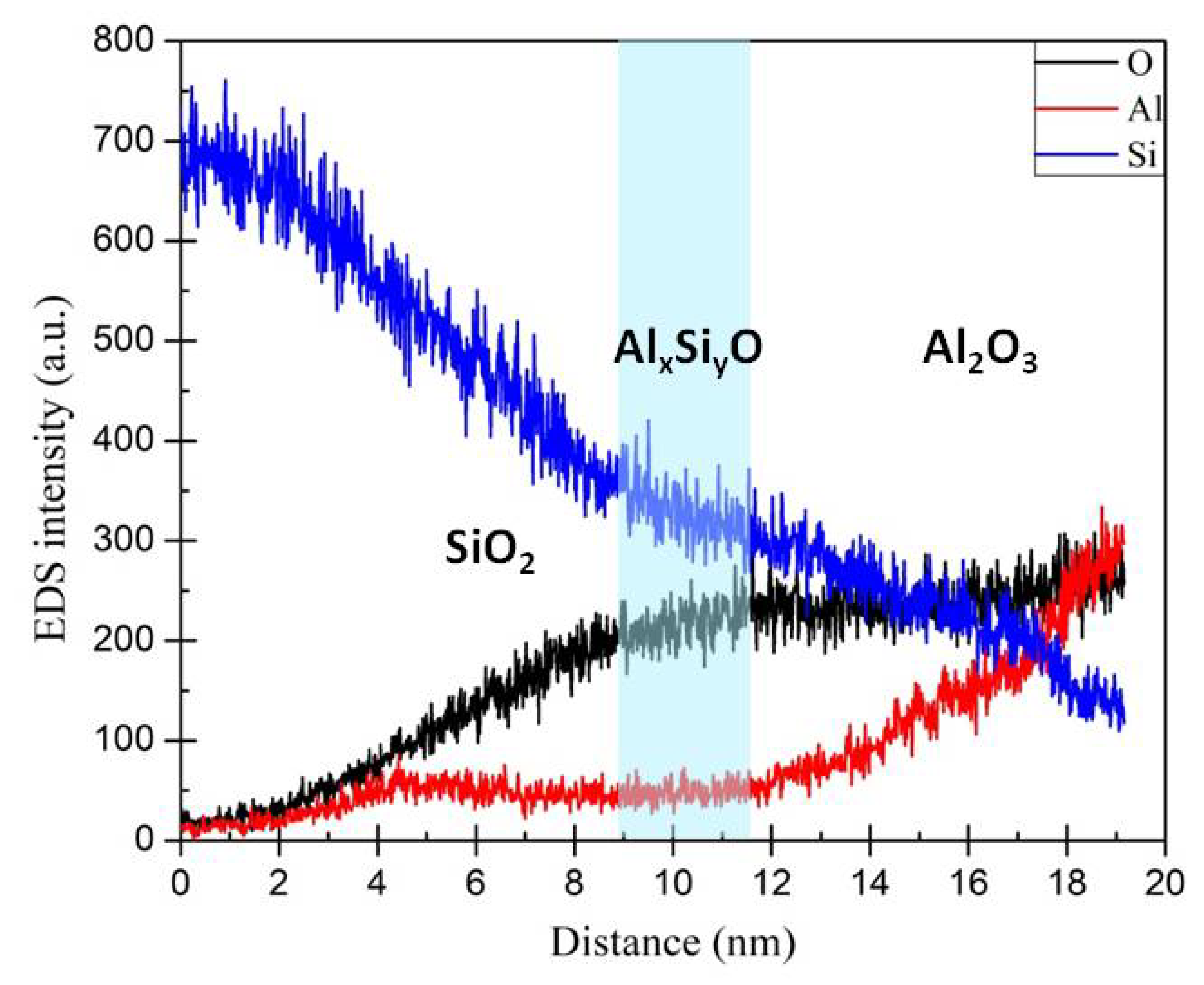
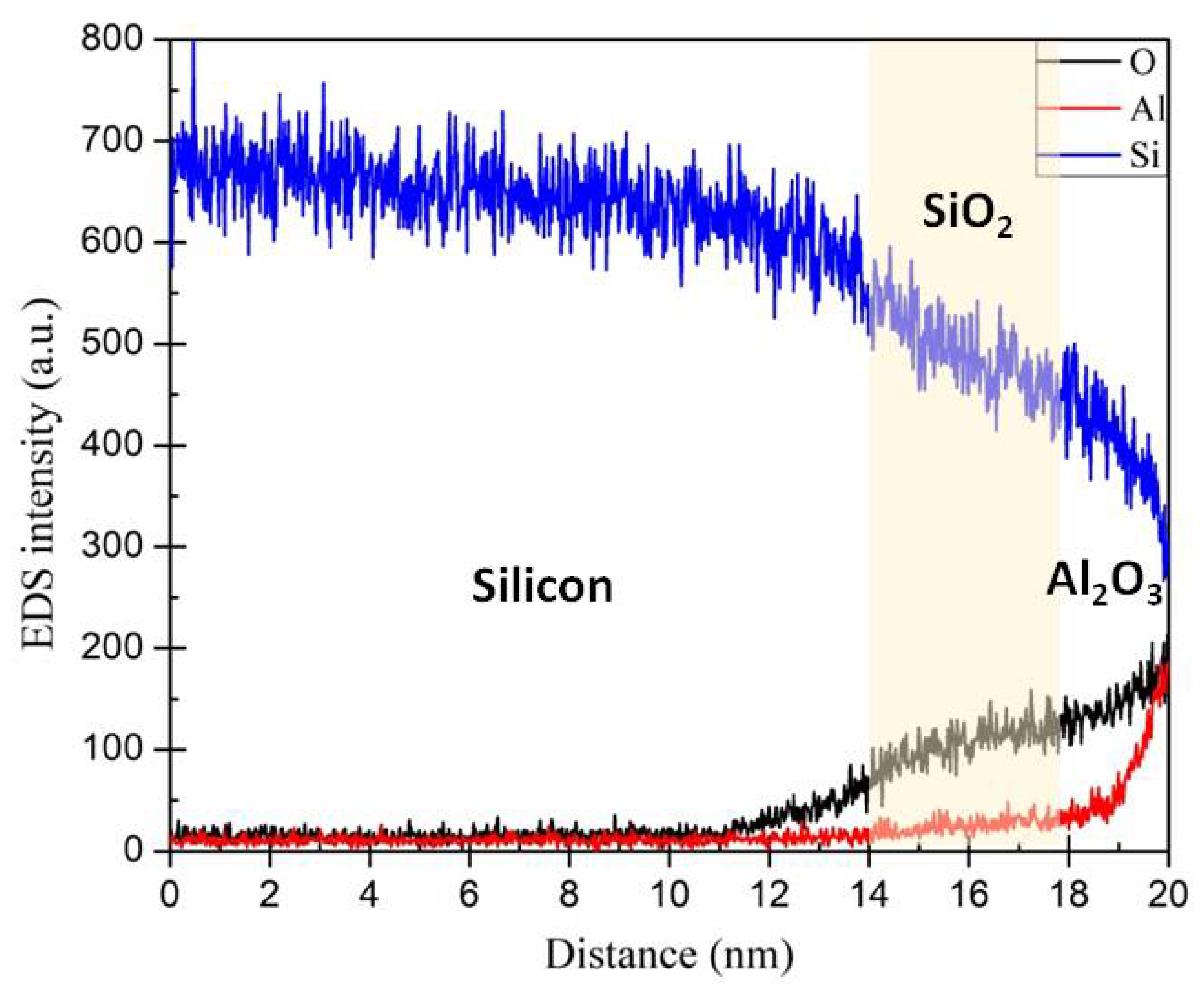
3.2. Energy-Dispersive Spectroscopy (EDS) Analysis

For the interface analysis, energy dispersive X-ray spectroscopy with a transmission electron microscope (TEM-EDS) was used to analyze the ALD-deposited Al2O3 material. From the EDS data shown in Figure 8 and Figure 9, noticeable changes in the film compositions were identified due to the annealing [30]. The different EDS line scans corresponding to Al Kα, O Kα, and Si Kα were extracted from the spectral image data [31]. According to the TEM image, other components in addition to SiO2 are discovered in the vicinity of the Si/Al2O3 interface when it was annealed at 200–400 °C as compared with the unannealed sample. When using the EDS to reveal the unknown constituents [32], Figure 8 shows that the interface subjecting to the 400 °C treatment contains an aluminosilicate AlxSiyO layer, which is further decomposed by the energy of high-temperature microwave annealing to form a SiOx and an Al2O3 layer [33]. In other words, the thermal diffusion and rearrangement of oxygen, aluminum, and silicon atoms all contribute to a distinct Si/SiO2/Al2O3 structure with a steep interface. The foregoing phenomenon has been improved as shown in Figure 9, when the microwave annealing temperature is elevated to 500 °C.

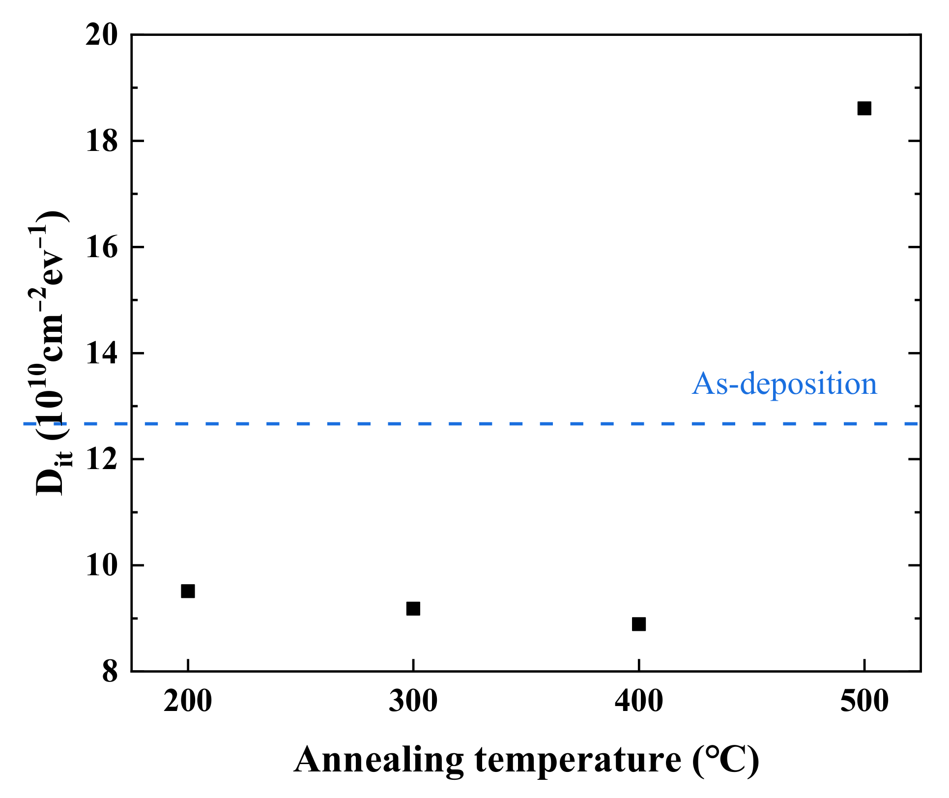
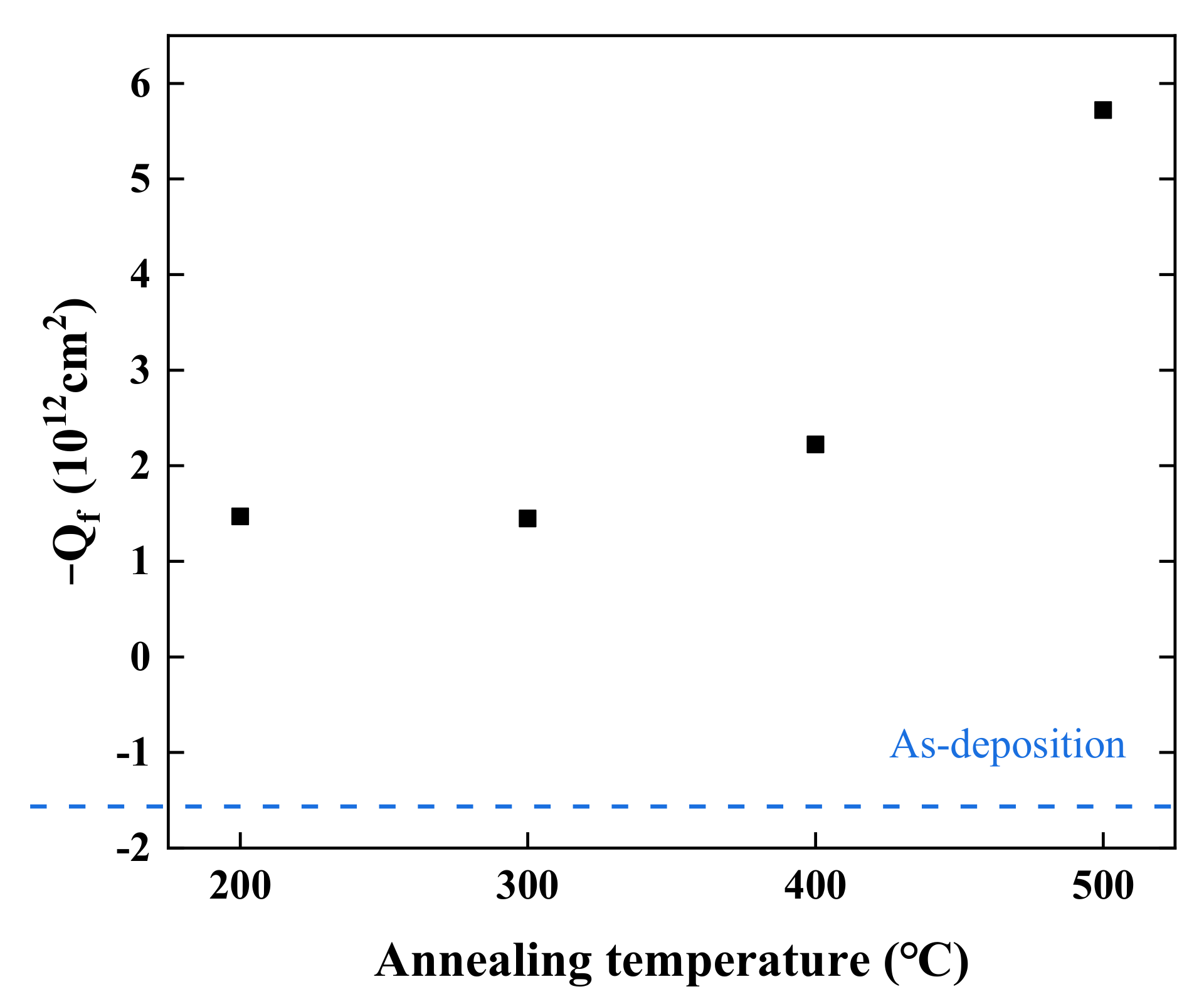
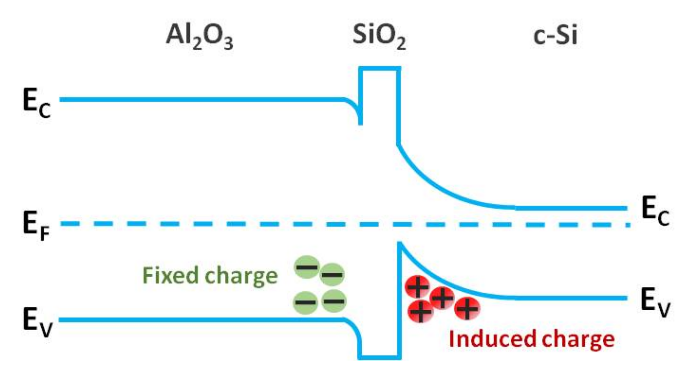
3.3. Capacitance-Voltage (C-V) Measurement

The capacitance-voltage (C-V) measurement was conducted in this research, and using the C-V measurement data, we can obtain the negative fixed charge situated at the interface. The method is based on calculating the relative dielectric constant εoxide of the oxide layer first with the use of the cumulative layer capacitance Cox formulated in Equation (3), and the negative charge density can be further determined by following the steps as sequentially revealed in Equations (3)–(6):
C o x = ε 0 ε o x i d e A t o x
where ε0 is the vacuum dielectric constant, tox is the thickness of the oxide layer, and A is the electrode area of the MIS structure. Then, Equation (4) is used to calculate LD (Debye length):
L D = ε s i ε 0 K T q 2 N a
where εsi is the relative permittivity of the silicon substrate, q is the unit charge, Na is the concentration of the silicon substrate, and T is the absolute temperature. The flat band capacitance CFB (F/cm2) is calculated with Equation (5):
C F B = 1 t o x ε 0 ε o x i d e + L D ε 0 ε s i
where ε0 is the vacuum dielectric constant, εoxide is the relative dielectric constant of the oxide layer, εsi is the relative dielectric constant of the silicon substrate, and tox is the thickness of the oxide layer. Then, from a particular point of the C-V curve that corresponds to the flat band voltage VFB, the fixed charge Qf (cm−2) can be calculated by Equation (6):
Q f = φ m s V F B C o x q A
where φms is the work function difference between the metal and the semiconductor, VFB is the flat band voltage, q is the unit charge, and A is the electrode area of the MIS structure.
As shown in Figure 10, initially the fixed charge is positive (Qf ~ 1.56 × 1012 cm−2) before attempting the microwave annealing, and as the microwave annealing temperature increases from 200 to 500 °C, Qf becomes negative, and the value of the so-called negative fixed charge, or −Qf, increases with the temperature. At the temperature of 200 and 300 °C, when the annealing energy provided is not sufficient, the respective values of Qf that are obtained, that is, −1.47 × 1012 cm−2 and −1.45 × 1012 cm−2, are virtually similar to one another. However, when the microwave annealing temperature is increased to 400 °C, the Qf value reaches −2.22 × 1012 cm−2, and the best −Qf obtained is −5.72 × 1012 cm−2 at 500 °C. The presence of the negative fixed charges critically affects the efficacy of the Al2O3 field passivation, which in turn can be elucidated using the band diagram of the Al2O3/SiO2/c-Si structure depicted in Figure 11 below. The negative fixed charges tend to induce the positive charges at the SiO2/c-Si interface. Judging the overall Qf values obtained, a high charge density is obtained from the Al2O3 deposited by the APALD equipment independently developed by our research team [34]. In addition, microwave annealing also contributes to the improvement in the quality of the SiO2 layer.
The interfacial trap density, Dit, is also obtained by adopting the conductance method shown in Equation (7) through C-V measurement [35]:
D i t = 2 ω C o x 2 G m a x q A { G m a x 2 + ω 2 C o x C m G m a x 2 }
Since the surface lattice defects of the silicon substrate seriously bring about unwanted electronic recombination, the importance of passivating the surface of the wafer, therefore, cannot be overemphasized. From the following Dit analysis results, it is clear that the oxygen in SiO2 film could combine with the dangling bonds on the silicon substrate to produce a chemical passivation effect. The use of APALD to deposit films is the key to delivering high-quality passivation. It can be seen from Figure 12 that Dit is 1 × 1011 cm−2 eV−1 before the film is annealed, and the lowest Dit achieved is 8.89 × 1010 cm−2 eV−1 when the film is annealed at 400 °C, whereas for other temperatures, Dit values of 9.51 × 1010 cm−2 eV−1, 9.18 × 1010 cm−2 eV−1, and 1.86 × 1011 cm−2 eV−1 are determined at 200, 300, and 500 °C, respectively. The non-thermal effect of microwave annealing also plays a significant role in the recrystallization and defect repair of silicon. When the recrystallization process is almost complete and the defects are mostly repaired, both the non-thermal and dielectric polarization loss effects are dramatically weakened. Microwave annealing can significantly reduce the peak temperature of silicon recrystallization or defect repair annealing within a shorter time frame, but the excess energy and time provided by microwave annealing could inexorably lead to the generation of traps and defects [29]. Thus, it becomes obvious that the defect density can be noticeably curtailed through the precise energy control of microwave annealing.

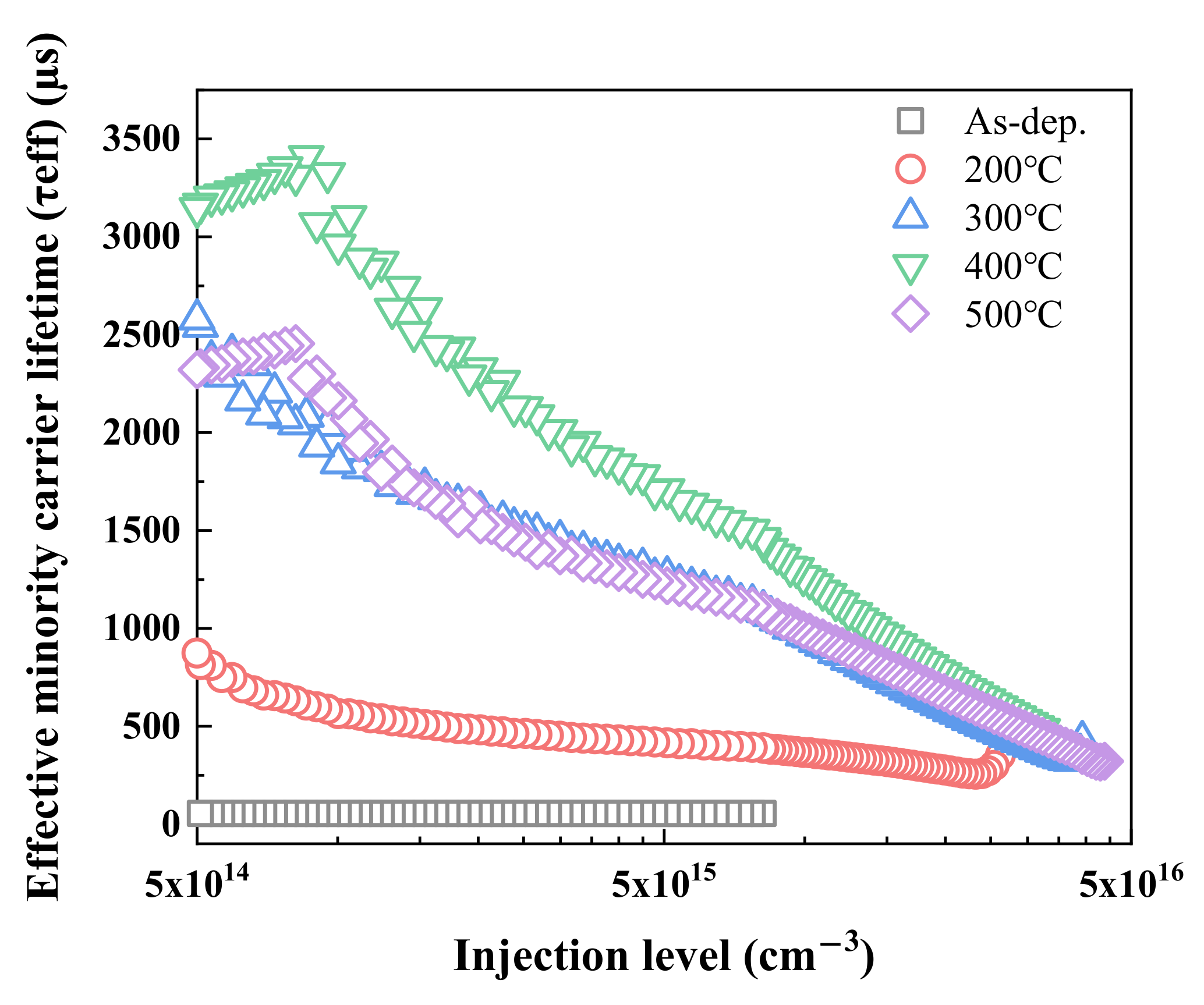
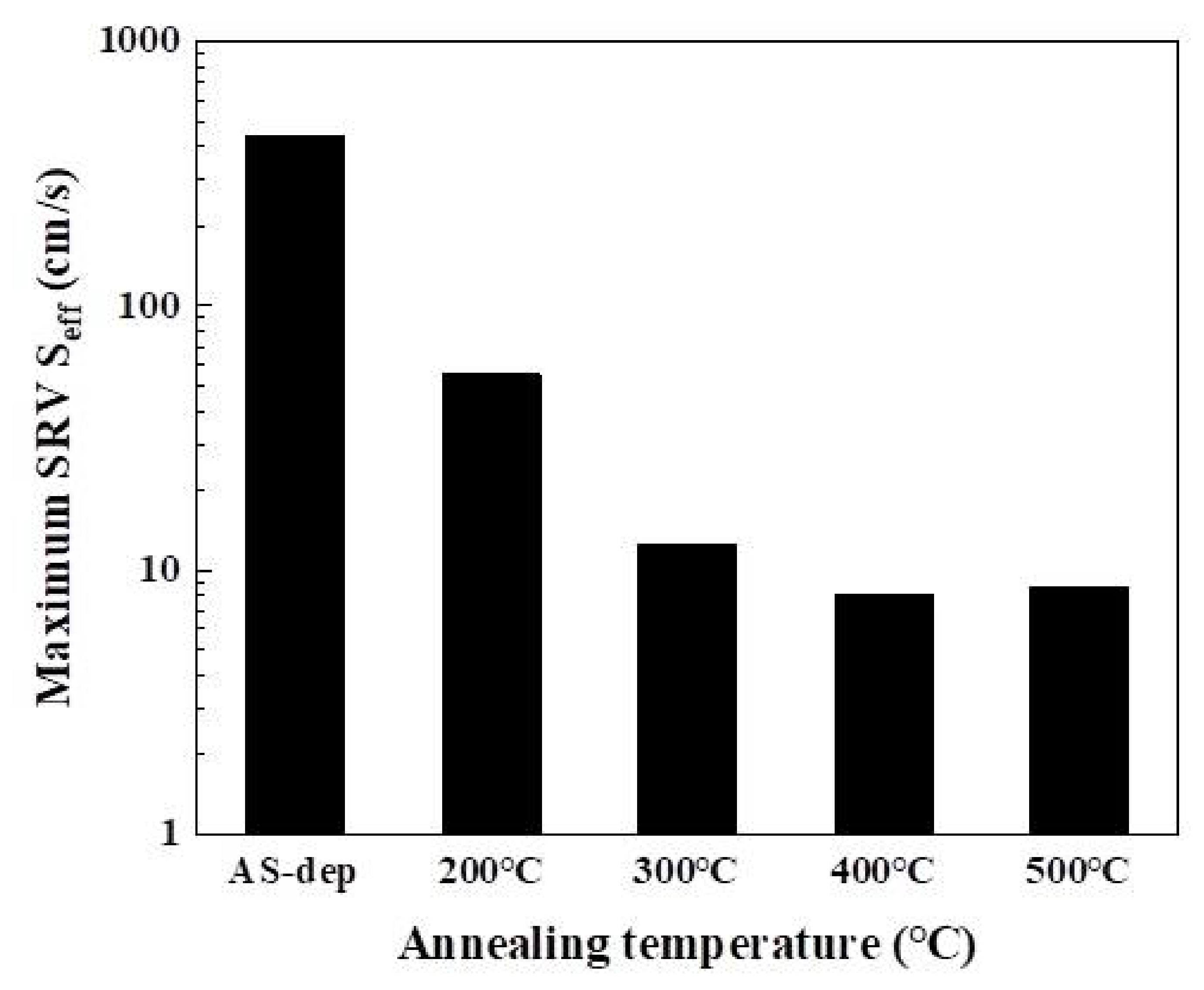
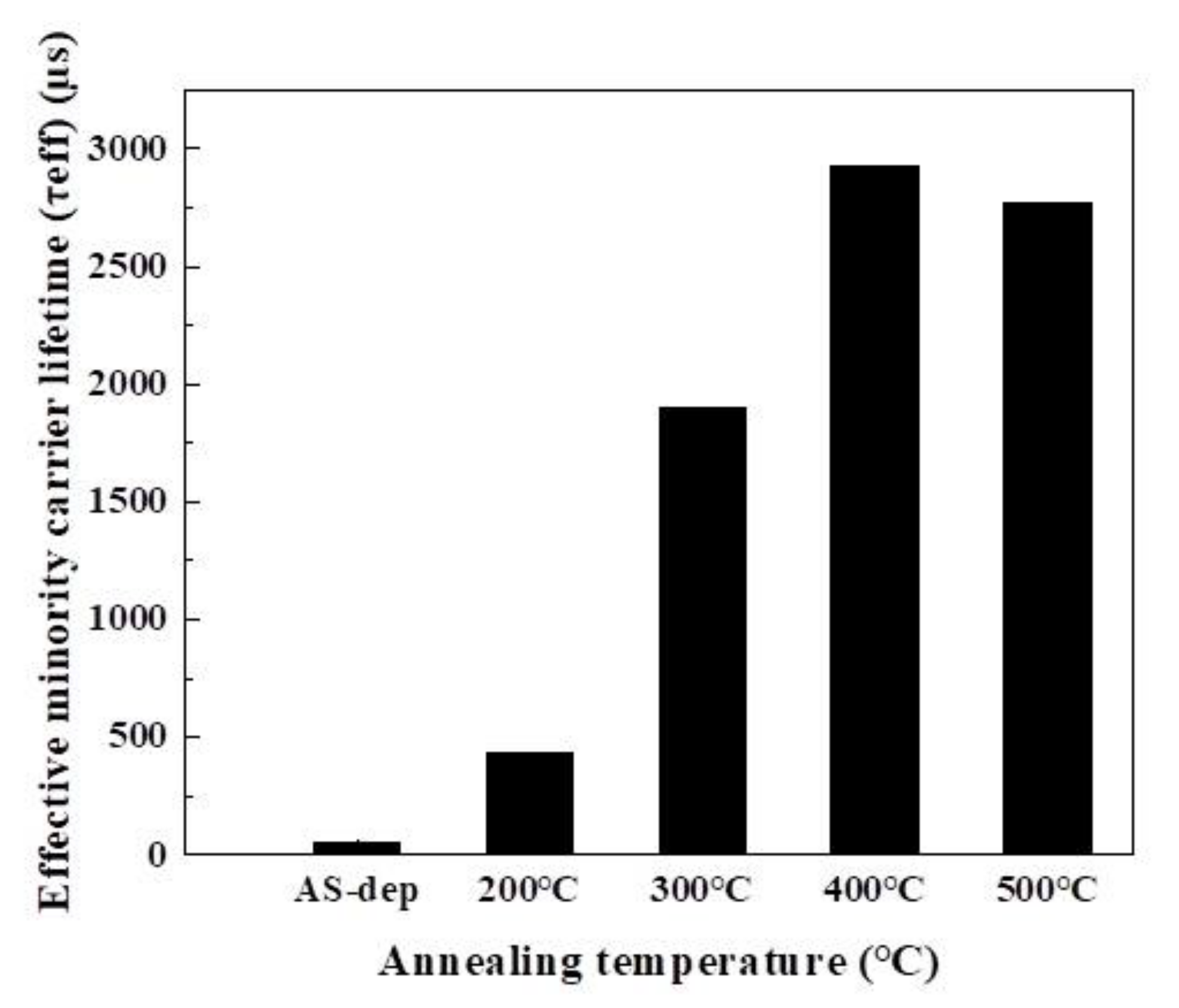
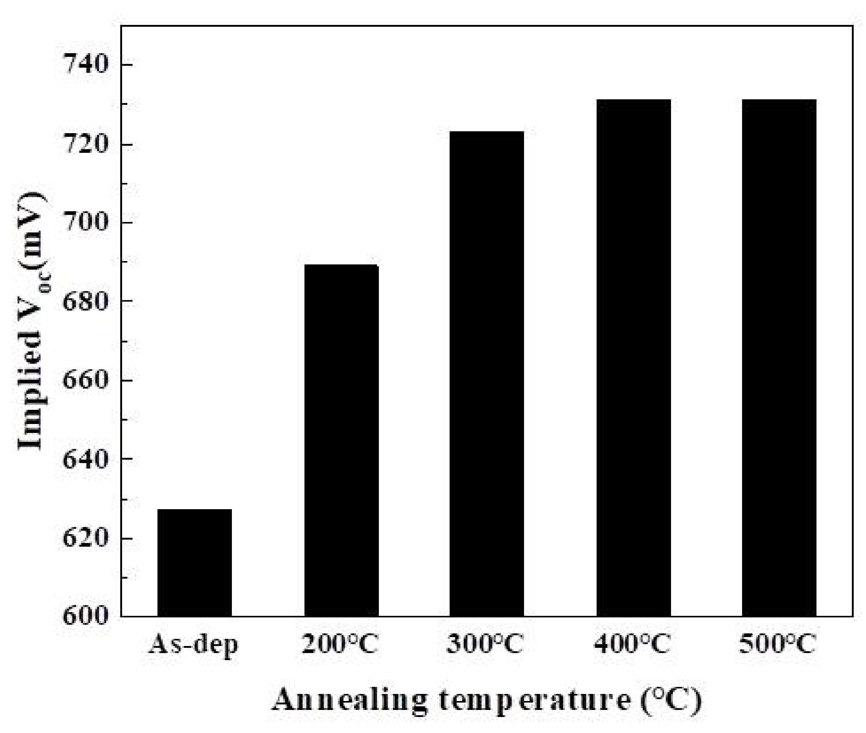
3.4. Quasi-Steady-State Photoconductance (QSSPC) Method

In this study, a silicon wafer lifetime tester (WCT-120, Sinton Consulting Inc., Boulder, CO, USA) was used to assess the effective minority carrier lifetime by operating in quasi-steady-state photoconductance (QSSPC) mode to confirm the efficacy of Al2O3 film passivation on P-type silicon wafers via APALD [36,37]. Figure 13 shows the evolution of the effective minority carrier lifetime (τeff) in response to various injection levels for Si/Al2O3 samples treated with different microwave annealing temperatures when compared with the one before annealing.
The values of τeff shown in Figure 14 are extracted under the high injection level of 5 × 1015 cm−3. It shows that τeff before annealing is only 54.60 μs, whereas at 400 °C, τeff becomes 2925.03 μs, which is the best result among all trials attempted, and in comparison, the other underperformed counterparts are 432.05 μs at 200 °C, 1895.59 μs at 300 °C, and 2772.97 μs at 500 °C. The effective minority carrier lifetime (τeff) is one of the most important indicators for evaluating the passivation effect, and this indicator can be used to determine the best process parameters for the post-annealing process. As a whole, by using the microwave annealing method, a long effective minority carrier lifetime (τeff) can be achieved with a relatively short annealing time and at a low temperature, which is all benefited from the unique microwave annealing mechanism and the non-thermal effect. Comparing microwave annealing with traditional furnace annealing, at least 75% of the time cost can be saved accordingly [18], which is very attractive for the commercial process of manufacturing solar cells.
The characteristics of τeff may be related to the bulk and surface recombination processes, which can be estimated by the following equation [38,39,40,41]:
1 τ e f f = 1 τ b u l k + 2 S e f f W
The τbulk in Equation (8) is considered as the bulk lifetime. According to the data provided by the wafer supplier, the τbulk for the P-type silicon wafer used in this research exceeds 4 ms, and W is the thickness of the wafer which is 475 μm. Because Seff is the effective surface recombination velocity (SRV), it is fair to assume that the two sides are equal for a symmetrical structure. The substrate used in this research is a high-quality silicon wafer material that has a very long τbulk, and τeff is mainly affected by surface recombination, so we can simplify Equation (9) to the following expression:
S e f f W 2 τ e f f
Figure 15 shows the maximum Seff value calculated by Equation (9). It can be seen from the trend that the recombination rate of the surface before annealing is very large, or about 434.98 cm/s whereas the lowest recombination rate is achieved at 400 °C, or only 8.12 cm/s. Relatively higher Seff values of 54.97 cm/s, 12.53 cm/s, and 8.56 cm/s are obtained at the annealing temperatures at 200, 300, and 500 °C, respectively. From a component point of view, the lower the SRV, the better the passivation effect of the surface, and the lower the number of carriers lost during the recombination process. Therefore, to minimize the surface recombination, it is better to chemically passivate the surface to reduce the interface defects by the order of magnitude. The extremely low SRV achieved for a sample annealed at 400 °C in the microwave environment implies that the high-quality Al2O3 film can be realized by APALD through the effective passivation of the dangling bonds on the surface of the silicon substrate.
The implied open-circuit voltage (IVoc) is used here as the third figure of merit to compare the quality of the selected dielectrics prepared by different deposition techniques for the effectiveness of passivating silicon surfaces, which can be calculated by inserting the τeffn) measured by QSSPC into the Equation (10) [42]:
I V o c = K T q ln Δ n p + Δ n n i , e f f 2
where Δn is the minority carrier concentration measured by WCT-120 under one sun condition, p is the hole concentration, and ni, eff is the intrinsic concentration.
Since this measurement is performed before the screen-printed electrode, this value is assumed to reflect the maximum Voc that can be achieved based on the internal material quality without optical loss or imperfect contact loss. It can be seen from Figure 16 that the evolution of IVoc virtually manifests the same trend as the τeff; therefore, for annealing implemented at 400 and 500 °C, the best IVoc obtained is 731 mV, whereas at 200 and 300 °C, the corresponding values are 689 and 723 mV, respectively. Compared with 627 mV before annealing, the importance of the annealing process can hardly be ignored. ALD deposited Al2O3 films are used as a passivation layer for PERC solar cells. The chemical passivation is designed to reduce the generation of dangling bonds on the wafer surface, whereas the microwave annealing provides suitable energy to optimize the τeff and IVoc values.

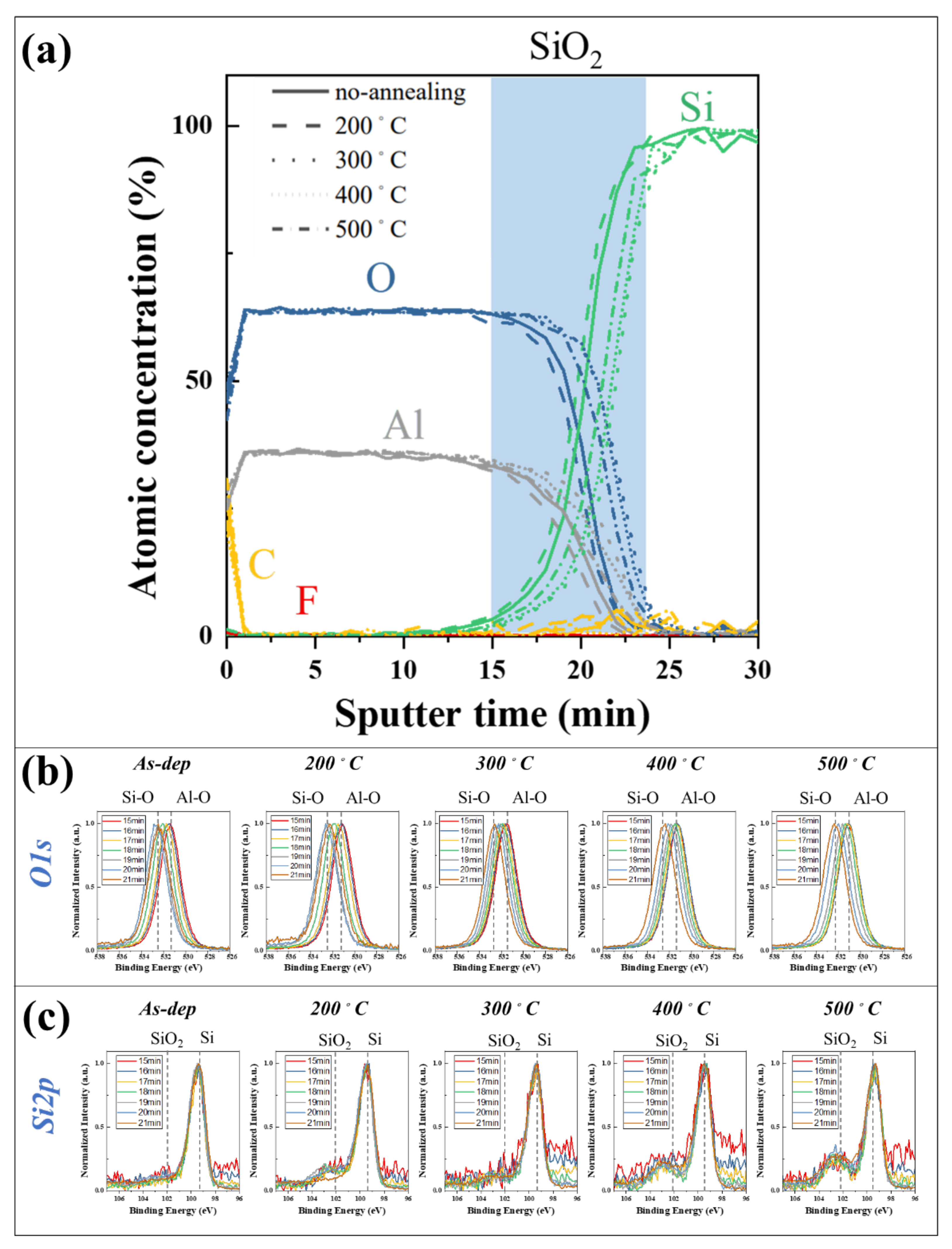
3.5. Surface Chemical Analysis (X-ray Photoelectron Spectroscopy)

To better understand the element ratio and element valence changes at different depths, XPS is used to conduct elemental depth analysis on samples under different annealing conditions. XPS uses an X-ray as the emission source to excite the inner shell electrons of the element as photoelectrons, and the subsequent kinetic energy of the photoelectron detected would reflect the magnitude of its binding energy. Different elements naturally have different binding energies. Based on this concept, the concentrations of the different elements can be estimated to achieve accurate quantitative analysis. For that matter, because the binding energies of different elements are expected to deviate from one another slightly, the valence states of the different elements can be identified. XPS not only can deliver two-dimensional surface scanning, but it can also couple with sputtering to perform one-dimensional in-depth analysis for interfacial probing as well. In this study, XPS was used for elemental depth analysis, focusing on the O1s and Si2p spectra at the interface, and observing the valence changes at the interface [43].
Figure 17 is the element ratio diagram of the depth analysis of the samples prepared under different annealing conditions. From the figure, it is observed that the Al:O ratio is about 2:3.4, and there is no significant difference between the two ratios after microwave annealing [7]. To better understand the valence information of the interface, the O1s and Si2p spectra corresponding to a sputtering time of 15~25 min are shown in Figure 17b,c, respectively. Note that both are normalized to better differentiate the valence change. From Figure 17b O1s spectrum, we observe that the binding energy (eV) of O1s increases with the depth, changing from 531 to 532.9 eV for all samples. The binding energy of 531 eV is identified with Al-O bonding whereas 532.9 eV is with Si-O bonding, all of which indicate that Al2O3 passivation film has been successfully prepared with APALD. In comparison, SiO2 film is produced at a sputtering time of 19–21 min. The above-mentioned EDS and TEM results are all consistent with one another [44]. Figure 17c shows the Si2p spectrum, from which the binding energy of 99.4 eV is identified as the Si element, whereas 103.5 eV is identified as the SiO2 signal. It is observed that the SiO2 layer is formed in the sample regardless of whether or not it has been annealed. XPS observations reveal the presence of SiO2 at the interface, the change in the valence state of O1s, and the element ratio of Al to O.

4. Conclusions

In this study, we used APALD independently developed by our group to deposit Al2O3 passivation film, and evaluated the efficacy of implementing the short-time microwave post-annealing process on sample passivation. By comparing the unannealed with the microwave-annealed samples treated at a temperature of 200–500 °C, the QSSPC analysis reveals that the longest effective carrier lifetime can be achieved when microwave annealing is performed at 400 °C for 5 min, of which τeff is 2925.03 μs, and the estimated Seff is 8.12 cm/s. These two important indicators are intimately related to the solar cell components. The passivation of the substrate dangling bond brought by microwave annealing was deemed excellent in terms of the relevant performance figures such as Dit of as low as 8.89 × 1010 cm−2 eV−1 at 400 °C and the IVoc value of as high as 731 mV. From the TEM image, a SiO2 layer was observed at the Si/Al2O3 interface, along with a detected change in the thickness of the SiO2 layer in response to the enhancement of microwave annealing energy. Moreover, SiO2 was the thinnest at 500 °C. At the same time, EDS and XPS were used to verify the existence of the SiO2 layer. The layer reflected the effect of field passivation, and the Qf value of −5.72 × 1012 cm−2 was verified through C-V analysis. Through XPS depth analysis, the ratio of Al:O is 2:3.4 was determined. APALD non-vacuum deposition has a high film deposition rate based on the verified thicknesses of the deposited films, which is deemed beneficial for an enhancement of the production rate and the cost reduction in vacuum equipment investment. Since the microwave relatively has a greater penetration depth during the annealing process, it uniquely provides uniform heating of an entire wafer, thereby bringing about the effect of rapid annealing when compared with traditional annealing methods. Based on a series of studies and analyses conducted by our team, applying microwave annealing to APALD-deposited aluminum oxide film ensures a fast process of producing good film characteristics, which further seals its applicability in the commercial arena.

Author Contributions

Conceptualization, Y.-C.H. and R.W.C.; methodology, Y.-C.H.; software, T.-C.W.; validation, Y.-C.H. and T.-C.W.; formal analysis, Y.-C.H. and R.W.C.; investigation, Y.-C.H.; resources, Y.-C.H. and K.-M.L.; data curation, Y.-C.H. and K.-M.L.; writing—original draft preparation, Y.-C.H.; writing—review and editing, K.-M.L. and R.W.C. All authors have read and agreed to the published version of the manuscript.

Funding

This research was funded by Bureau of Energy, Ministry of Economic Affairs, R.O.C., grant number: 110-D0105.

Institutional Review Board Statement

Not applicable.

Informed Consent Statement

Not applicable.

Data Availability Statement

Data is contained within the article.

Conflicts of Interest

The authors declare no conflict of interest.

References

  1. Blakers, A. Development of the PERC Solar Cell. IEEE J. Photovolt. 2019, 9, 629–635. [Google Scholar] [CrossRef]
  2. Barar, A.; Manaila-Maximean, D. Ruthenium-based DSSC efficiency optimization by grapheme quantum dot doping. Univ. Politeh. Buchar. Sci. Bull. Ser. A Appl. Math. Phys. 2021, 2, 309–316. [Google Scholar]
  3. Barar, A.; Manaila-Maximean, D.; Danila, O.; Vladescu, M. Parameter extraction of an organic solar cell using asymptotic estimation and Lambert W function. In Advanced Topics in Optoelectronics, Microelectronics, and Nanotechnologies VIII; SPIE—International Society for Optics and Photonics: Constanta, Romania, 2016; Volume 10010, p. 1001034. [Google Scholar]
  4. Hannebauer, H.; Dullweber, T.; Baumann, U.; Falcon, T.; Brendel, R. 21.2%-efficient fineline-printed PERC solar cell with 5 busbar front grid. Phys. Status Solidi Rapid Res. Lett. 2014, 8, 675–679. [Google Scholar] [CrossRef]
  5. Ye, F.; Deng, W.; Guo, W.; Liu, R.; Chen, D.; Chen, Y.; Yang, Y.; Yuan, N.; Ding, J.; Feng, Z.; et al. 22.13% Efficient Industrial p-Type Mono PERC Solar Cell. In Proceedings of the IEEE 43rd Photovoltaic Specialists Conference, Portland, OR, USA, 5–10 June 2016; IEEE: New York, NY, USA. [Google Scholar] [CrossRef]
  6. Zhang, L.; Jiang, H.C.; Liu, C.; Dong, J.W.; Chow, P. Annealing of Al2O3 thin films prepared by atomic layer deposition. J. Phys. D 2007, 40, 3707–3713. [Google Scholar] [CrossRef]
  7. Naumann, V.; Otto, M.; Wehrspohn, R.B.; Hagendorf, C. Chemical and structural study of electrically passivating Al2O3/Si interfaces prepared by atomic layer deposition. J. Vac. Sci. Technol. B 2012, 30, 04D106-1–04D106-6. [Google Scholar] [CrossRef]
  8. Lei, D.; Yu, X.; Song, L.; Gu, X.; Li, G.; Yang, D. Modulation of atomic-layer-deposited Al2O3 film passivation of silicon surface by rapid thermal processing. Appl. Phys. Lett. 2011, 99, 052103. [Google Scholar] [CrossRef]
  9. Cast, P.S.; Heo, Y.H.; Billot, E.; Olwal, P.; Hofmann, M.; Rentsch, J.; Glunz, S.W.; Preu, R. Variation of the layer thickness to study the electrical property of PECVD Al2O3 / c-Si interface. Energy Procedia 2011, 8, 642–647. [Google Scholar] [CrossRef]
  10. Saint-Cast, P.; Kania, D.; Heller, R.; Kuehnhold, S.; Hofmann, M.; Rentsch, J.; Preu, R. High-temperature stability of c-Si surface passivation by thick PECVD Al2O3 with and without hydrogenated capping layers. Appl. Surf. Sci. 2012, 258, 8371–8376. [Google Scholar] [CrossRef]
  11. Schmidt, J.; Wernera, F.; Veith, B.; Zielke, D.; Steingrube, S.; Altermatt, P.P.; Gatz, S.; Dullweber, T.; Brendel, R. Advances in the Surface Passivation of Silicon Solar Cells. Energy Procedia 2012, 15, 30–39. [Google Scholar] [CrossRef] [Green Version]
  12. Nowicki, R.S. Properties of rfsputtered Al2O3 films deposited by planar magnetron. J. Vac. Sci. Technol. 1977, 14, 127–133. [Google Scholar] [CrossRef]
  13. Edlmayr, V.; Moser, M.; Walter, C.; Mitterer, C. Thermal stability of sputtered Al2O3 coatings. Surf. Coat. Technol. 2010, 204, 1576–1581. [Google Scholar] [CrossRef]
  14. Hu, B.; Yao, M.; Xiao, R.; Chen, J.; Yao, X. Optical properties of amorphous Al2O3 thin films prepared by a sol-gel process. Ceram. Int. 2014, 40, 14133–14139. [Google Scholar] [CrossRef]
  15. Cibert, C.; Hidalgo, H.; Champeaux, C.; Tristant, P.; Tixier, C.; Desmaison, J.; Catherinot, A. Properties of aluminum oxide thin films deposited by pulsed laser deposition and plasma enhanced chemical vapor deposition. Thin Solid Films 2008, 516, 1290–1296. [Google Scholar] [CrossRef]
  16. Jakschik, S.; Avellan, A.; Schroeder, U.; Bartha, J.W. Influence of Al2O3 Dielectrics on the Trap-Depth Profiles in MOS Devices Investigated by the Charge-Pumping Method. IEEE Trans. Electron. Devices 2004, 51, 2252–2255. [Google Scholar] [CrossRef]
  17. Thomas, S.; Nalini, S.; Kumar, K.R. Microwave plasma-assisted ALD of Al2O3 thin films: A study on the substrate temperature dependence of various parameters of interest. Appl. Phys. A 2017, 123, 185. [Google Scholar] [CrossRef]
  18. Huang, Y.-C.; Chuang, R.W. Study on Annealing Process of Aluminum Oxide Passivation Layer for PERC Solar Cells. Coatings 2021, 11, 1052. [Google Scholar] [CrossRef]
  19. Vahdatifar, S.; Mortazavi, Y.; Khodadadi, A.A. Atmospheric pressure atomic layer deposition of iron oxide nanolayer on the Al2O3/SiO2/Si substrate for mmtall vertically aligned CNTs growth. J. Mater. Sci. 2020, 55, 13634–13657. [Google Scholar] [CrossRef]
  20. Hoye, R.L.Z.; Muñoz-Rojas, D.; Nelson, S.F.; Illiberi, A.; Poodt, P.; Roozeboom, F.; MacManus-Driscoll, J.L. Research Update: Atmospheric pressure spatial atomic layer deposition of ZnO thin films: Reactors, doping, and devices. APL Mater. 2015, 3, 040701. [Google Scholar] [CrossRef]
  21. Levy, D.H.; Nelson, S.F.; Freeman, D. Oxide Electronics by Spatial Atomic Layer. J. Display Technol. 2009, 5, 484–494. [Google Scholar] [CrossRef]
  22. Guo, J.; Wang, D.; Xu, Y.; Zhu, X.; Wen, K.; Miao, G.; Cao, W.; Si, J.; Lu, M.; Guo, H. Secondary electron emission characteristics of Al2O3 coatings prepared by atomic layer deposition. AIP Adv. 2019, 9, 095303. [Google Scholar] [CrossRef]
  23. Zhu, B.; Wu, X.; Liu, W.-J.; Ding, S.-J.; Zhang, D.W.; Fan, Z. Dielectric Enhancement of Atomic Layer-Deposited Al2O3/ZrO2/Al2O3 MIM Capacitors by Microwave Annealing. Nano Lett. 2019, 14, 53. [Google Scholar] [CrossRef]
  24. Bhattacharya, M.; Basak, T. A review on the susceptor assisted microwave processing of materials. Energy 2016, 97, 306–338. [Google Scholar] [CrossRef]
  25. Hsu, C.H.; Huang, C.W.; Cho, Y.S.; Wu, W.Y.; Wuu, D.S.; Zhang, X.Y.; Zhu, W.Z.; Lien, S.Y.; Ye, C.S. Efficiency improvement of PERC solar cell using an aluminum oxide passivation layer prepared via spatial atomic layer deposition and post annealing. Surf. Coat. Technol. 2019, 358, 968–975. [Google Scholar] [CrossRef]
  26. Lee, Y.-J.; Chuang, S.-S.; Hsueh, F.-K.; Lin, H.-M.; Wu, S.-C.; Wu, C.-Y.; Tseng, T.-Y. Dopant Activation in Single-Crystalline Germanium by Low-Temperature Microwave Annealing. IEEE Electron. Device Lett. 2011, 32, 194–196. [Google Scholar] [CrossRef]
  27. Song, K.; Koo, C.Y.; Jun, T.; Lee, D.; Jeong, Y.; Moon, J. Low-temperature soluble InZnO thin film transistors by microwave annealing. J. Cryst. Growth 2011, 326, 23–27. [Google Scholar] [CrossRef]
  28. Fu, C.; Wang, Y.; Xu, P.; Yue, L.; Sun, F.; Zhang, D.W.; Zhang, S.-L.; Luo, J.; Zhao, C.; Wu, D. Understanding the microwave annealing of silicon. AIP Adv. 2017, 7, 035214. [Google Scholar] [CrossRef] [Green Version]
  29. Lee, Y.-J.; Cho, T.-C.; Chuang, S.-S.; Hsueh, F.-K.; Lu, Y.-L.; Sung, P.-J.; Chen, H.-C.; Current, M.I.; Tseng, T.-Y.; Chao, T.-S.; et al. Low-Temperature Microwave Annealing Processes for Future IC Fabrication—A Review. IEEE Trans. Electron Devices 2014, 61, 651–665. [Google Scholar] [CrossRef]
  30. Ziegler, J.; Otto, M.; Sprafke, A.N.; Wehrspohn, R.B. Activation of Al2O3 passivation layers on silicon by microwave annealing. Appl. Phys. A 2013, 113, 285–290. [Google Scholar] [CrossRef]
  31. Yue, L.; Fu, C.-C.; Sun, F.; Qiu, Z.-J.; Zhang, S.-L.; Wu, D. Microwave Annealing as a Low Thermal Budget Technique for ZnO Thin-Film Transistors Fabricated Using Atomic Layer Deposition. IEEE Electron. Device Lett. 2017, 38, 1390–1393. [Google Scholar] [CrossRef]
  32. Shi, S.; Qian, S.; Hou, X.; Mu, J.; He, J.; Chou, X. Structural and Optical Properties of Amorphous Al2O3 Thin Film Deposited by Atomic Layer Deposition. Adv. Condens. Matter Phys. 2018, 2018, 7598978. [Google Scholar] [CrossRef] [Green Version]
  33. Djebaili, K.; Mekhalif, Z.; Boumaza, A.; Djelloul, A. XPS, FTIR, EDX, and XRD Analysis of Al2O3 Scales Grown on PM2000 Alloy. J. Spectrosc. 2015, 2015, 868109. [Google Scholar] [CrossRef] [Green Version]
  34. Glunz, S.W.; Preu, R.; Biro, D. Crystalline Silicon Solar Cells. In Comprehensive Renewable Energy; Sayigh, A., Ed.; Elsevier: Amsterdam, The Netherlands, 2012; pp. 353–387. [Google Scholar] [CrossRef]
  35. Lale, A.; Scheid, E.; Cristiano, F.; Datas, L.; Reig, B.; Launay, J.; Temple-Boyer, P. Study of aluminium oxide thin films deposited by plasmaenhanced atomic layer deposition from tri-methyl-aluminium and dioxygen precursors: Investigation of interfacial and structural properties. Thin Solid Films 2018, 666, 20–27. [Google Scholar] [CrossRef] [Green Version]
  36. Sinton, R.A. Contactless determination of current–voltage characteristics and minority-carrier lifetimes in semiconductors from quasi-steady-state photoconductance data. Appl. Phys. Lett. 1996, 69, 2510. [Google Scholar] [CrossRef]
  37. Demaurex, B.; Seif, J.P.; Smit, S.; Macco, B.; Kessels, W.M.M.; Geissbühler, J.S.; Wolf, D.; Ballif, C. Atomic Layer Deposited Transparent Electrodes for Silicon Heterojunction Solar Cells. IEEE J. Photovolt. 2014, 4, 1387–1396. [Google Scholar] [CrossRef]
  38. Goodarzi, M.; Sinton, R.; Macdonald, D. Quasi-steady-state photoconductance bulk lifetime measurements on silicon ingots with deeper photogeneration. AIP Adv. 2019, 9, 015128. [Google Scholar] [CrossRef] [Green Version]
  39. Kontermann, S.; Wolf, A.; Reinwand, D.; Grohe, A.; Biro, D.; Preu, R. Optimizing annealing steps for crystalline silicon solar cells with screen printed front side metallization and an oxide-passivated rear surface with local contacts. Prog. Photovolt Res. Appl. 2009, 17, 554–566. [Google Scholar] [CrossRef]
  40. Dauwe, S.; Schmidt, J.; Hezel, R. Very low surface recombination velocities on p- and n-type silicon wafers passivated with hydrogenated amorphous silicon films. In Proceedings of the Twenty-Ninth IEEE Photovoltaic Specialists Conference, New Orleans, LA, USA, 19–24 May 2002; IEEE: New York, NY, USA. [Google Scholar] [CrossRef]
  41. Lelièvre, J.-F.; Fourmond, E.; Kaminski, A.; Palais, O.; Ballutaud, D.; Lemiti, M. Study of the composition of hydrogenated silicon nitride SiNx:H for efficient surface and bulk passivation of silicon. Sol. Energy Mater Sol. Cells 2009, 93, 1281–1289. [Google Scholar] [CrossRef] [Green Version]
  42. Wang, X.; Juhl, M.; Abbott, M.; Hameiri, Z.; Yao, Y.; Lennon, A. Use of QSSPC and QSSPL to monitor recombination processes in p-type silicon solar cells. Energy Procedia 2014, 55, 169–178. [Google Scholar] [CrossRef] [Green Version]
  43. Werner, F.; Veith, B.; Zielke, D.; Kühnemund, L.; Tegenkamp, C.; Seibt, C.; Brendel, R.; Schmidt, J. Electronic and chemical properties of the c-Si/Al2O3 interface. J. Appl. Phys. 2011, 109, 113701. [Google Scholar] [CrossRef]
  44. Cho, M.; Park, H.B.; Park, J.; Hwang, C.S.; Lee, J.-C.; Oh, S.-J.; Jeong, J.K.; Hyun, S.; Kang, H.-S.; Kim, Y.-W.; et al. Thermal annealing effects on the structural and electrical properties of HfO2 / Al2O3 gate dielectric stacks grown by atomic layer deposition on Si substrates. J. Appl. Phys. 2003, 94, 2563. [Google Scholar] [CrossRef]
Figure 1. Al2O3 film growth via APALD process flow chart.
Coatings 11 01450 g001
Figure 2. Schematic diagram of APALD equipment.
Coatings 11 01450 g002
Figure 3. Illustration of working principle of APCVD equipment deposited film.
Coatings 11 01450 g003
Figure 4. Schematic of the atomic layer deposition process.
Coatings 11 01450 g004
Figure 5. The illustrations of the traditional annealing and microwave annealing mechanisms.
Coatings 11 01450 g005
Figure 6. TEM images of the microwave-annealed Si/Al2O3 samples at different temperatures: (a) As-deposit, (b) 200 °C, (c) 300 °C, (d) 400 °C, and (e) 500 °C.
Coatings 11 01450 g006
Figure 7. (a) The resultant Al2O3 and (b) SiO2 film thicknesses under different microwave annealing conditions.
Coatings 11 01450 g007
Figure 8. EDS line scans of the Si/Al2O3 samples being microwave-annealed at 400 °C.
Coatings 11 01450 g008
Figure 9. EDS line scans of the Si/Al2O3 samples being microwave-annealed at 500 °C.
Coatings 11 01450 g009
Figure 10. The values of the negative fixed charge (−Qf) extracted from the C-V measurement for Al/Al2O3/Si MIS samples treated under different microwave annealing conditions.
Coatings 11 01450 g010
Figure 11. Energy band diagram of Al2O3/SiO2/c-Si structure.
Coatings 11 01450 g011
Figure 12. C-V measurement was conducted to extract the interfacial trap density (Dit) of Al/Al2O3/Si MIS samples under different microwave annealing conditions.
Coatings 11 01450 g012
Figure 13. The measured effective minority carrier lifetime (τeff) in response to different injection levels for Si/Al2O3 samples treated with different annealing conditions.
Coatings 11 01450 g013
Figure 14. Effective minority carrier lifetime of Si/Al2O3 samples treated with different annealing temperatures under the carrier injection of 5 × 1015 cm−3.
Coatings 11 01450 g014
Figure 15. Effective surface recombination rate of Si/Al2O3 samples using P-type wafers being treated with different annealing temperatures.
Coatings 11 01450 g015
Figure 16. The implied open-circuit voltage of Si/Al2O3 samples being treated with different annealing temperature conditions.
Coatings 11 01450 g016
Figure 17. XPS depth analysis of samples under different annealing conditions: (a) Element ratio diagram (Sputter time 15~25 min); (b) O1s signal; (c) Si2p signal.
Coatings 11 01450 g017
Table 1. Deposition parameters of the APALD Al2O3 layer.
ParametersValue
Substrate temperature (°C)140
TMA temperature (°C)17.5
H2O temperature (°C)45
Pipe Temperature (°C)70
TMA flow rate (sccm)300
H2O flow rate (sccm)500
RUN_Cycles110
Thickness (nm)10
Table 2. Parameters for samples annealed at different microwave power.
Annealing ConditionTemperature (°C)
150 W, 5 min200
500 W, 20 min300
600 W, 20 min400
800 W, 20 min500
Publisher’s Note: MDPI stays neutral with regard to jurisdictional claims in published maps and institutional affiliations.

