
Obliquely Bideposited TiN Thin Film with Morphology-Dependent Optical Properties


Abstract
:1. Introduction
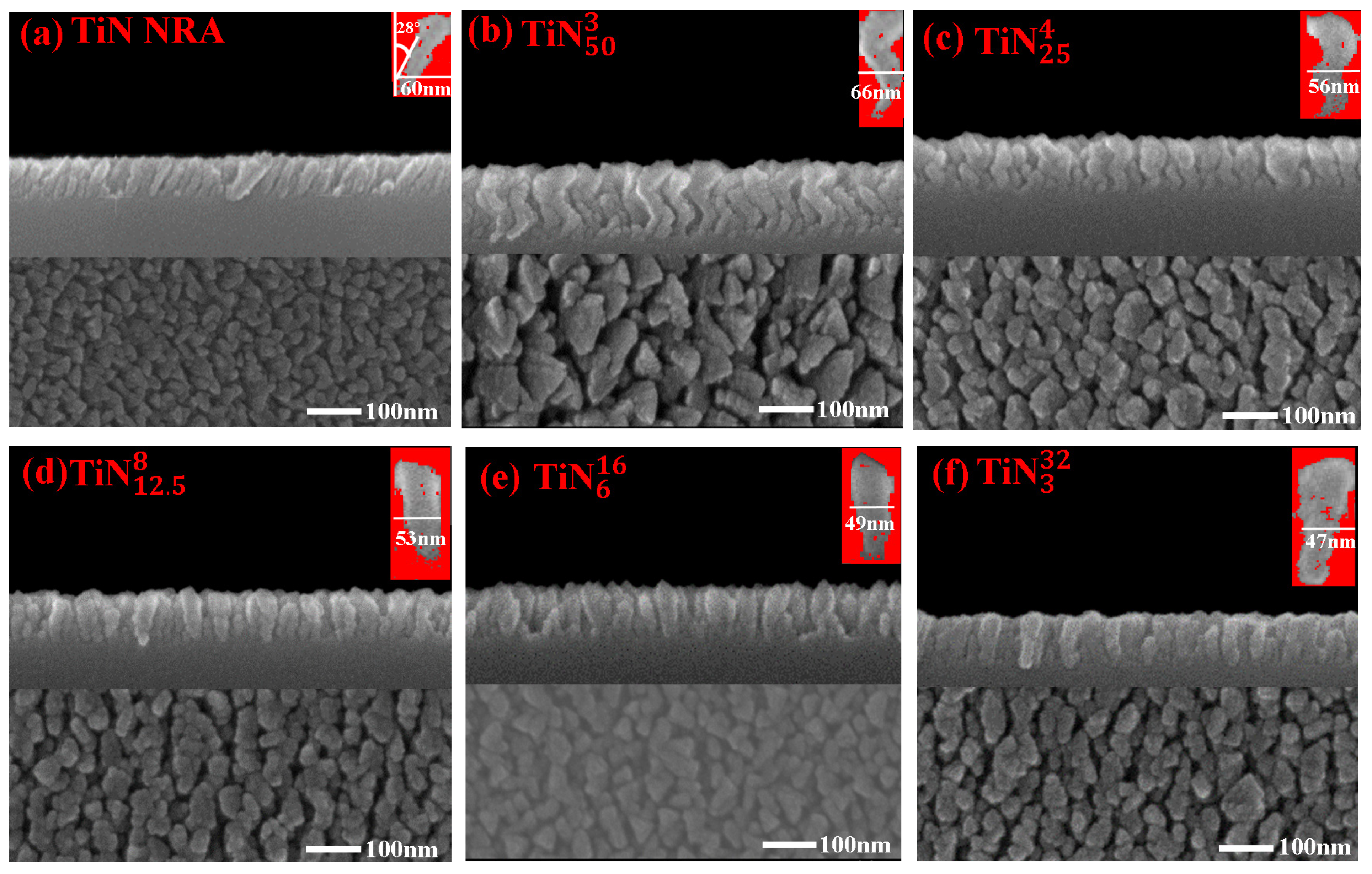
2. Fabrication
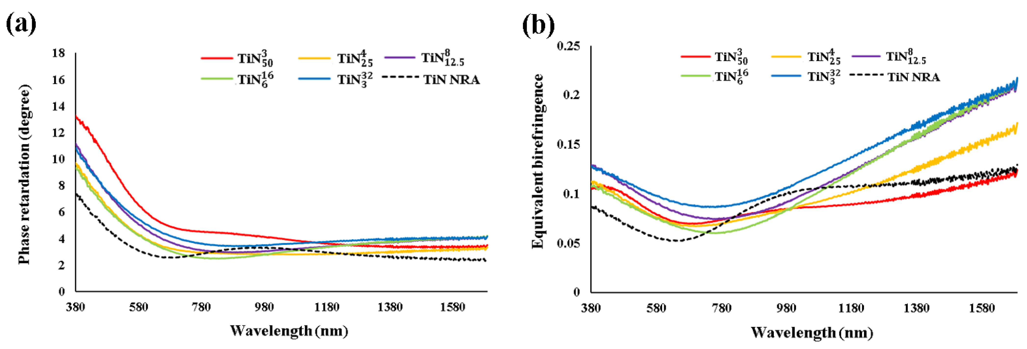
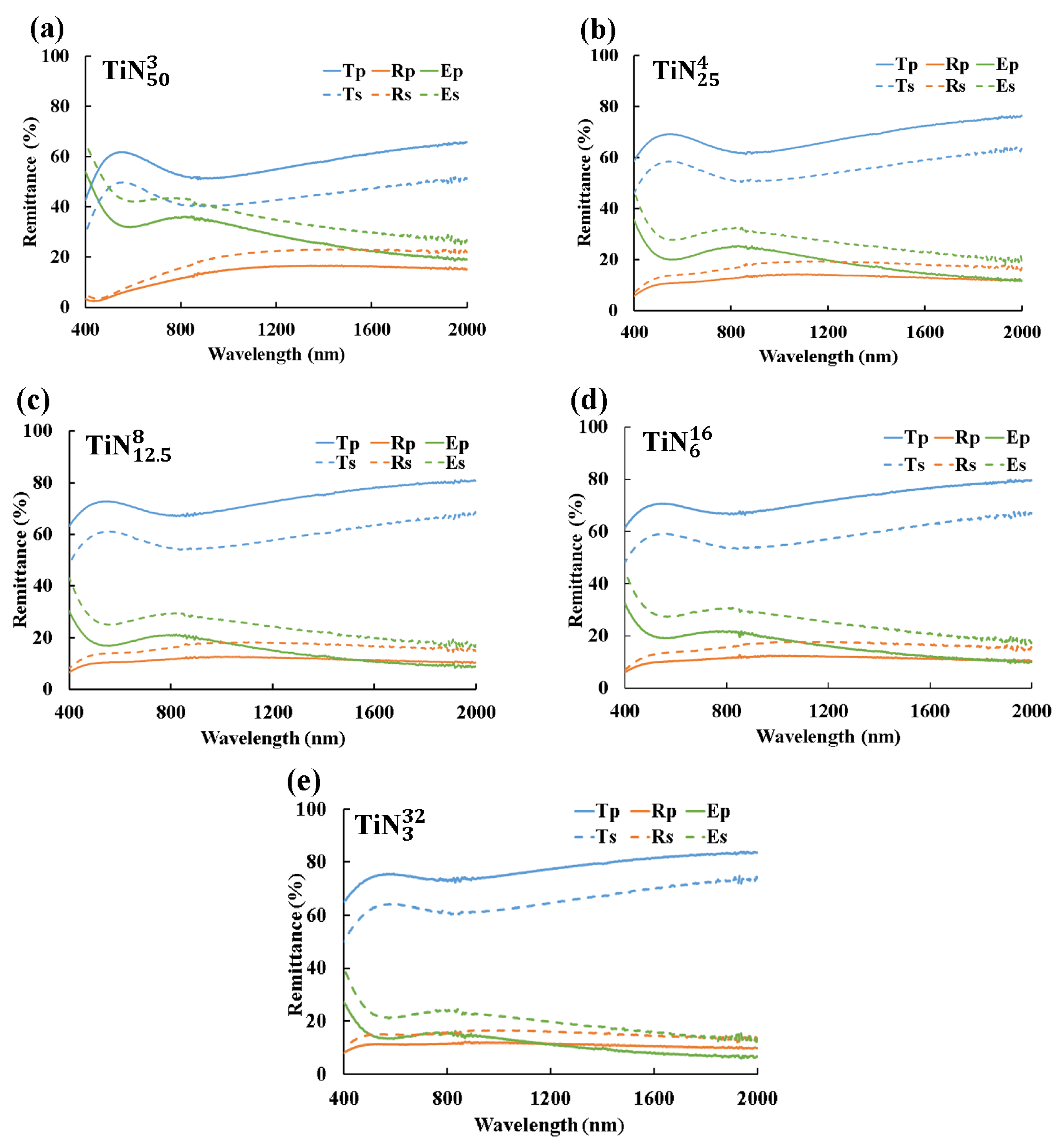
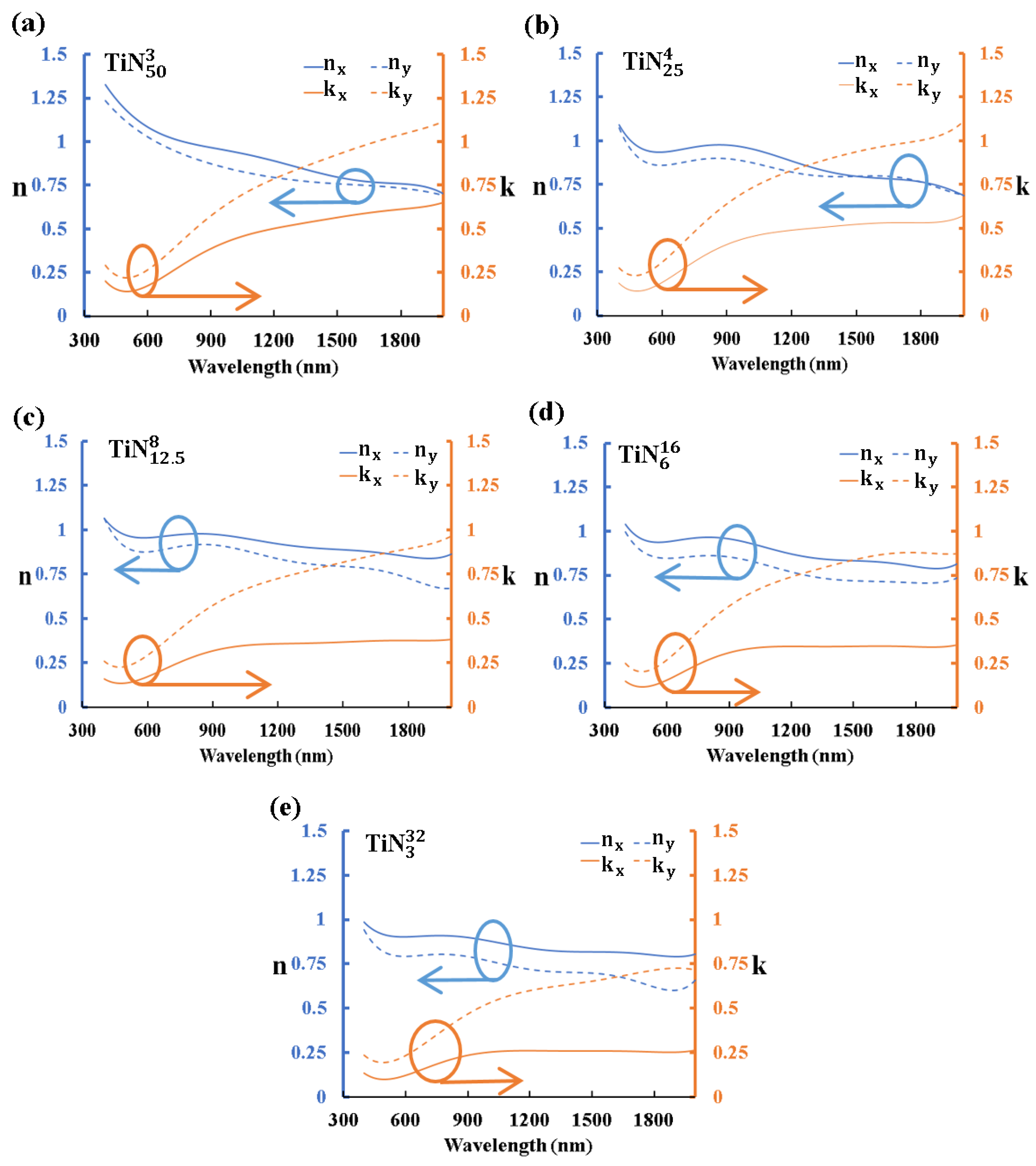
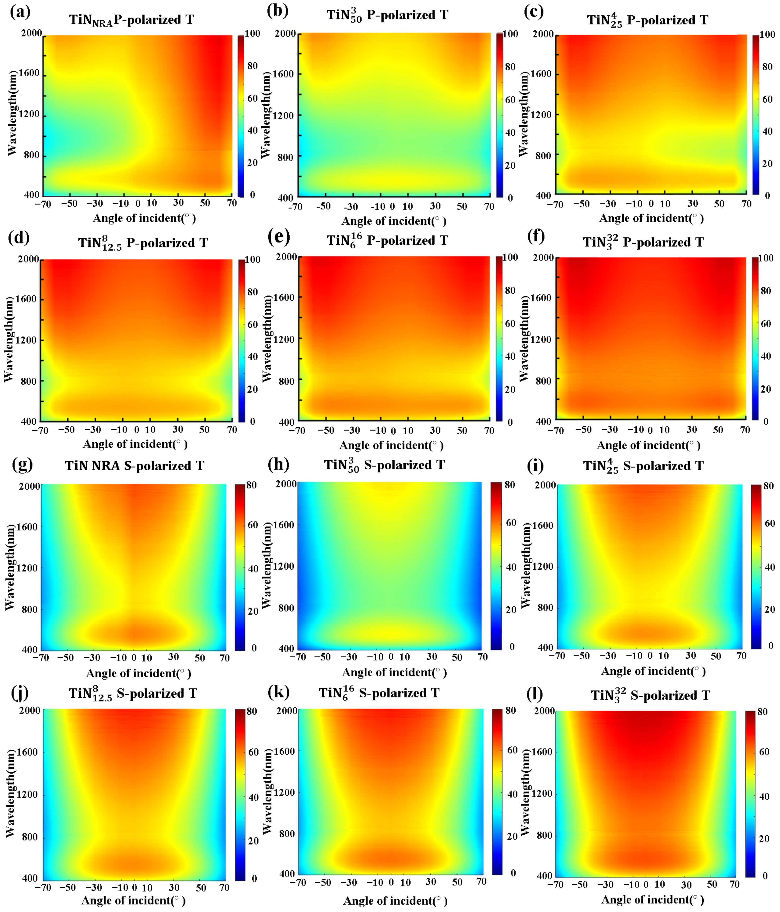
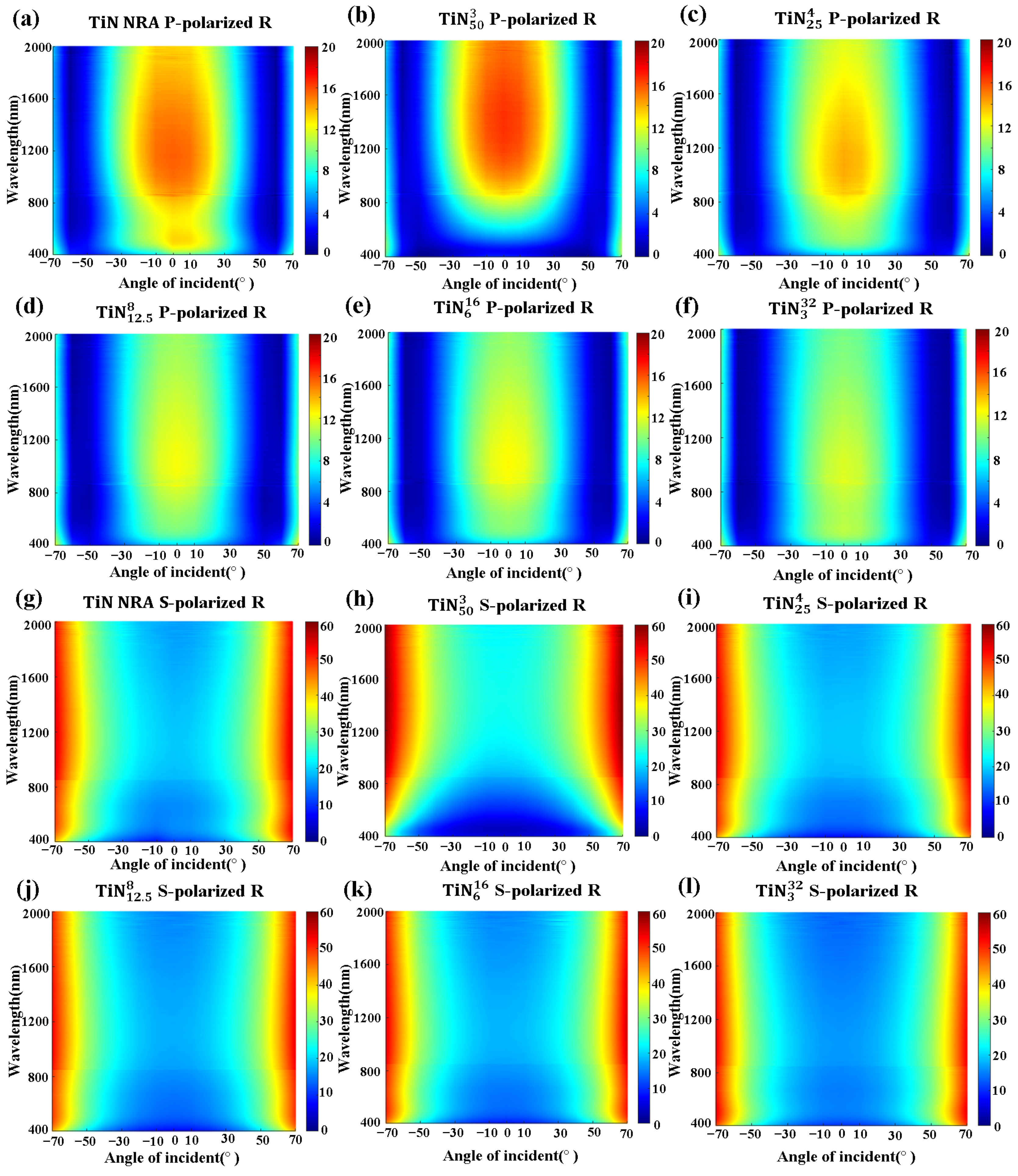
3. Measurement and Discussion
4. Conclusions
Author Contributions
Funding
Institutional Review Board Statement
Informed Consent Statement
Data Availability Statement
Conflicts of Interest
References
- Guler, U.; Shalaev, V.M.; Boltasseva, A. Nanoparticle plasmonics: Going practical with transition metal nitrides. Mater. Today 2015, 18, 227–237. [Google Scholar] [CrossRef]
- Korobenko, A.; Saha, S.; Godfrey, A.T.K.; Gertsvolf, M.; Naumov, A.Y.; Villeneuve, D.M.; Boltasseva, A.; Shalaev, V.M.; Corkum, P.B. High-harmonic generation in metallic titanium nitride. Nat. Commun. 2021, 12, 4981. [Google Scholar] [CrossRef] [PubMed]
- Zhou, J.; Chen, X.; Guo, L.J. Efficient thermal–light interconversions based on optical topological transition in the metal-dielectric multilayered metamaterials. Adv. Mater. 2016, 28, 3017–3023. [Google Scholar] [CrossRef] [PubMed] [Green Version]
- Boltasseva, A.; Atwater, H.A. Low-loss plasmonic metamaterials. Science 2011, 331, 290–291. [Google Scholar] [CrossRef]
- Guler, U.; Boltasseva, A.; Shalaev, V.M. Refractory plasmonics. Science 2014, 344, 263–264. [Google Scholar] [CrossRef]
- Pogrebnjak, A.; Smyrnova, K.; Bondar, O. Nanocomposite multilayer binary nitride coatings based on transition and refractory metals: Structure and properties. Coatings 2019, 9, 155. [Google Scholar] [CrossRef] [Green Version]
- Pierson, H.O. Handbook of Refractory Carbides and Nitrides; William Andrew: Norwich, NY, USA, 1996. [Google Scholar]
- Farrell, I.L.; Reeves, R.J.; Preston, A.R.H.; Ludbrook, B.M.; Downes, J.E.; Ruck, B.J.; Durbin, S.M. Tunable electrical and optical properties of hafnium nitride thin films. Appl. Phys. Lett. 2010, 96, 071914. [Google Scholar] [CrossRef] [Green Version]
- Hu, C.; Gu, Z.; Wang, J.; Zhang, K.; Zhang, X.; Li, M.; Zhang, S.; Fan, X.; Zheng, W. Nature of tunable optical reflectivity of rocksalt hafnium nitride films. J. Phys. Chem. C 2014, 118, 20511–20520. [Google Scholar] [CrossRef]
- Zgrabik, C.M.; Hu, E.L. Optimization of sputtered titanium nitride as a tunable metal for plasmonic applications. Opt. Mater. Express 2015, 5, 2786–2797. [Google Scholar] [CrossRef] [Green Version]
- Qin, F.; Chen, X.; Yi, Z.; Yao, W.; Yang, H.; Tang, Y.; Yi, Y.; Li, H.; Yi, Y. Ultra-broadband and wide-angle perfect solar absorber based on TiN nanodisk and Ti thin film structure. Sol. Energy Mater. Sol. C 2020, 211, 110535. [Google Scholar] [CrossRef]
- Li, W.; Guler, U.; Kinsey, N.; Naik, G.V.; Boltasseva, A.; Guan, J.; Shalaev, V.M.; Kildishev, A.V. Refractory plasmonics with titanium nitride: Broadband metamaterial absorber. Adv. Mater. 2014, 26, 7959–7965. [Google Scholar] [CrossRef]
- Jen, Y.J.; Yang, K.B.; Lin, P.C.; Chung, M.H. Deposited ultra-thin titanium nitride nanorod array as a plasmonic near-perfect light absorber. Sci. Rep. 2020, 10, 22269. [Google Scholar] [CrossRef] [PubMed]
- Hodgkinson, I.J.; Wu, Q.H. Birefringent Thin Films and Polarizing Elements; World Scientific Publishing Company: Singapore, 1998. [Google Scholar]
- Bairagi, S.; Järrendahl, K.; Eriksson, F.; Hultman, L.; Birch, J.; Hsiao, C.L. Glancing angle deposition and growth mechanism of inclined AlN nanostructures using reactive magnetron sputtering. Coatings 2020, 10, 768. [Google Scholar] [CrossRef]
- Martin, P.M. Handbook of Deposition Technologies for Films and Coatings; William Andrew: Norwich, NY, USA, 2010; pp. 621–670. [Google Scholar]
- Badshah, M.A.; Koh, N.Y.; Zia, A.W.; Abbas, N.; Zahra, Z.; Saleem, M.W. Recent developments in plasmonic nanostructures for metal enhanced fluorescence-based biosensing. Nanomaterials 2020, 10, 1749. [Google Scholar] [CrossRef]
- Park, Y.J.; Sobahan, K.M.A.; Hwangbo, C.K. Optical properties of TiO2 zigzag films prepared by using oblique angle deposition. J. Korean Phys. Soc. 2010, 56, 1378–1381. [Google Scholar]
- Hodgkinson, I.; Wu, Q.H. Serial bideposition of anisotropic thin films with enhanced linear birefringence. Appl. Opt. 1999, 38, 3621–3625. [Google Scholar] [CrossRef]
- Jen, Y.J.; Liu, W.C.; Cong, M.Y.; Chan, T.L. Bideposited silver nanocolloid arrays with strong plasmon-induced birefringence for SERS application. Sci. Rep. 2020, 10, 20143. [Google Scholar] [CrossRef]
- Guler, U.; Zemlyanov, D.; Kim, J.; Wang, Z.; Chandrasekar, R.; Meng, X.; Stach, E.; Kildishev, A.V.; Shalaev, V.M.; Boltasseva, A. Plasmonic titanium nitride nanostructures via nitridation of nanopatterned titanium dioxide. Adv. Opt. Mater. 2017, 5, 1600717. [Google Scholar] [CrossRef]
- Dick, B.; Brett, M.J.; Smy, T.; Belov, M.; Freeman, M.R. Periodic submicrometer structures by sputtering. J. Vac. Sci. Technol. B 2001, 19, 1813. [Google Scholar] [CrossRef]
- Jen, Y.J.; Chan, T.L.; Liao, B.H.; Li, Z.X.; Liu, W.C.; Cong, M.Y. Tunable plasmonic resonances in TiN nanorod arrays. Coatings 2019, 9, 863. [Google Scholar] [CrossRef] [Green Version]
- Fischer, R.; Galeb, B.T.; Yoder, P. Optical System Design, 2nd ed.; McGraw-Hill Education: New York, NY, USA, 2008. [Google Scholar]
- Yadav, J.; Raturi, P.; Yadav, S.; Singh, J.P. Zig-zag Ag2S nanostructures for superior optical absorption and photoelectrochemical water splitting performance. Renew. Energy 2021, 179, 2256–2266. [Google Scholar] [CrossRef]


| Samples | Average Width of Nanozigzag (nm) | Thicknesses (nm) | Deposition Time (min) |
|---|---|---|---|
| 60 | 90.4 | 396 | |
| 66 | 132.52 | 608 | |
| 56 | 91.09 | 408 | |
| 53 | 91.45 | 408 | |
| 49 | 91.35 | 408 | |
| 47 | 89.67 | 408 |
Publisher’s Note: MDPI stays neutral with regard to jurisdictional claims in published maps and institutional affiliations. |
© 2021 by the authors. Licensee MDPI, Basel, Switzerland. This article is an open access article distributed under the terms and conditions of the Creative Commons Attribution (CC BY) license (https://creativecommons.org/licenses/by/4.0/).
Share and Cite
Jen, Y.-J.; Ma, W.-C.; Lin, T.-Y. Obliquely Bideposited TiN Thin Film with Morphology-Dependent Optical Properties. Coatings 2021, 11, 1418. https://doi.org/10.3390/coatings11111418
Jen Y-J, Ma W-C, Lin T-Y. Obliquely Bideposited TiN Thin Film with Morphology-Dependent Optical Properties. Coatings. 2021; 11(11):1418. https://doi.org/10.3390/coatings11111418
Chicago/Turabian StyleJen, Yi-Jun, Wei-Chieh Ma, and Ting-Yen Lin. 2021. "Obliquely Bideposited TiN Thin Film with Morphology-Dependent Optical Properties" Coatings 11, no. 11: 1418. https://doi.org/10.3390/coatings11111418
APA StyleJen, Y.-J., Ma, W.-C., & Lin, T.-Y. (2021). Obliquely Bideposited TiN Thin Film with Morphology-Dependent Optical Properties. Coatings, 11(11), 1418. https://doi.org/10.3390/coatings11111418