Article

Effect of HfO2-Based Multi-Dielectrics on Electrical Properties of Amorphous In-Ga-Zn-O Thin Film Transistors

1
Ministry Education Key Laboratory of Physical Electronics and Devices, School of Electronic Science and Engineering, Xi’an Jiaotong University, Xi’an 710049, China
2
School of Automation, Xi’an University of Posts and Telecommunications, Xi’an 710049, China
3
Hunan Institute of Advanced Sensing and Information Technology, Xiangtan University, Xiangtan 411105, China
4
National Key Laboratory of Application Specific Integrated Circuit, Hebei Semiconductor Research Institute, Shijiazhuang 050051, China
5
Key Laboratory of the Ministry of Education, International Center for Dielectric Research, School of Electronic Science and Engineering, Xi’an Jiaotong University, Xi’an 710049, China
*
Authors to whom correspondence should be addressed.
Coatings 2021, 11(11), 1381; https://doi.org/10.3390/coatings11111381
Submission received: 8 October 2021 / Revised: 7 November 2021 / Accepted: 9 November 2021 / Published: 11 November 2021
(This article belongs to the Special Issue New Advances in Thin-Film Transistor)

Abstract

:
We report the fabrication of bottom gate a-IGZO TFTs based on HfO2 stacked dielectrics with decent electrical characteristics and bias stability. The microscopic, electrical, and optical properties of room temperature deposited a-IGZO film with varied oxygen content were explored. In order to suppress the bulk defects in the HfO2 thin film and hence maximize the quality, surface modification of the SiNx film was investigated so as to achieve a more uniform layer. The root mean square (RMS) roughness of SiNx/HfO2/SiNx (SHS) stacked dielectrics was only 0.66 nm, which was reduced by 35% compared with HfO2 single film (1.04 nm). The basic electrical characteristics of SHS-based a-IGZO TFT were as follows: Vth is 2.4 V, μsat is 21.1 cm2 V−1 s−1, Ion/Ioff of 3.3 × 10⁷, Ioff is 10−11 A, and SS is 0.22 V/dec. Zr-doped HfO2 could form a more stable surface, which will decrease the bulk defect states so that the stability of device can be improved. It was found that the electrical characteristics were improved after Zr doping, with a Vth of 1.4 V, Ion/Ioff of 108, μsat of 19.5 cm2 V−1 s−1, Ioff of 10−12 A, SS of 0.18 V/dec. After positive gate bias stress of 104 s, the ΔVth was decreased from 0.43 V (without Zr doping) to 0.09 V (with Zr doping), the ΔSS was decreased from 0.19 V/dec to 0.057 V/dec, respectively, which shows a meaningful impact to realize the long-term working stability of TFT devices.

1. Introduction

In recent years, with the development of flat panel display (FPD), the traditional cathode ray tube (CRT) display has been gradually eliminated, which is replaced by liquid crystal display (LCD) and organic light emitting diode (OLED). With the updating of intelligent mobile phones and other portable electronic products, OLED technology has developed rapidly. Compared with LCD, OLED has the advantages of active lighting, high contrast, ultra-thin, low power consumption, wide viewing angle, and fast response speed, and is easy to realize flexible display and 3D display [1,2]. However, unlike LCD, OLED is a current driving device, the pixel units emit light through current injection, which requires high mobility TFT to provide high current. Recently, oxide semiconductor TFTs represented by amorphous InGaZnO (a-IGZO) have been widely studied with higher carrier mobility (>10 cm2 V−1 s−1) and switching current ratio (>107), which can meet the requirements of OLEDs for mobility, response speed, and driving current [3,4,5]. At the same time, it also has the advantages of low temperature preparation, high visible light transparency, good uniformity, and illumination stability [6]. Meanwhile, a-IGZO TFT also has some drawbacks. For example, a-IGZO film is easy to react with water vapor and movable ions in the air, which lead to the movement of threshold voltage (Vth), resulting in poor repeatability and stability of the device [7,8]. However, this instability can be improved by TFT device structure [9], dielectric material selection [10], and post-processing [11,12].
As we know, low power consumption is a significant advantage of OLED. The reduction of TFT driving voltage, that is to say, using high dielectric constant (high k) materials, is the most effective way to realize lower power consumption of OLED. High k materials such as HfO2 [13], Al2O3 [14], Y2O3 [15] can reduce the equivalent oxide layer thickness (EOT). However, high-k dielectrics have some inherent defects, such as high leakage current, poor surface morphology, high trap charge density, and these defects will deteriorate the device characteristics and degrade the long-term stability. The trade of between improving the dielectric constant and keeping long-term working stability is a key point for promoting the application of a-IGZO TFT in FPD.
In this paper, we have studied the process and device characteristics of a-IGZO TFT based on HfO2 stacked dielectrics. The microscopic, electrical and optical properties of a-IGZO film were studied. Then, combined with HfO2 film deposited by magnetron sputtering and SiNx film deposited by PE-CVD, a more uniform and smooth stacked dielectrics were achieved, TFT with HfO2/SiNx (HS) and SiNx/HfO2/SiNx (SHS) dielectrics realized decent device characteristics with high mobility, high switching current ratio, and low threshold voltage. The stability of device under positive gate bias is preliminarily verified. The research can provide experimental reference for the application of high-k dielectrics a-IGZO TFT in new flat panel display.

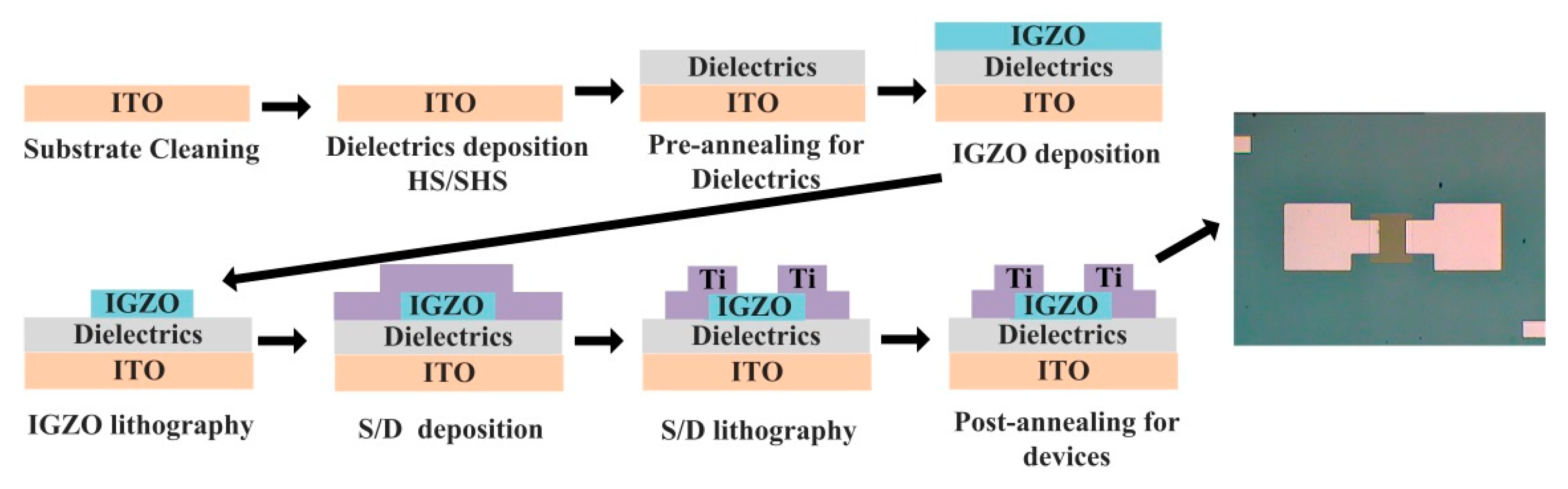
2. Materials and Methods

The device preparation process is shown in Figure 1. The ITO glass is used as the substrate and gate material for preparing the a-IGZO TFT, the film resistivity is 10–15 ohm/sq (Zhuhai Kaivo Optoelectronic Technology Co., Ltd., Zhuhai, China). The substrate is cleaned by standard RCA method. TFT devices with HfO2/SiNx (HS) and SiNx/HfO2/SiNx (SHS) stacked dielectrics are prepared in this study, SiNx and HfO2 films are deposited by PECVD (Plasma-Enhanced Chemical Vapor Deposition, PED-301, Anelva, Japan) and RF magnetron sputtering (ACS-4000-C4, ULVAC, Japan), respectively. The parameters are shown in Table 1, then stacked dielectrics are annealed at 300 °C (ULVAC, RTP-6) in N2 atmosphere to repair the interfaces (e.g., bulks, dangling bonds). a-IGZO film is deposited by DC magnetron sputtering at room temperature, the power is 100 W, film thickness is 60 nm, argon flow is 30 sccm, oxygen flow is varied from 0 to 5 sccm. Atomic Force Microscopy (AFM, SPI, 3800-SPA-400, Japan) and Scanning Electron Microscopy (SEM, Quanta, F250, USA) are used to characterize a-IGZO surface morphology and roughness. X-Ray Diffraction (XRD, Shimadzu XRD-7000, Japan) are used to obtain the crystal orientation. The composition, proportion, and binding energy of a-IGZO film are tested by X-ray photoelectron spectroscopy (XPS, Kratos AXIS ULTRA, UK). Titanium (Ti) that is deposited by DC magnetron sputtering and patterned by lift-off process is used as source and drain (S/D) electrodes due to its good ohmic contact with a-IGZO film [16]. At last, the post-annealing is applied with the temperature of 350 °C, the heating rate of 2 °C/s, the holding time of 10 min in order to improve the device stability. I-V and C-V characteristics are tested by Keithley 4200 semiconductor characterization system.

3. Results and Discussions

3.1. a-IGZO Fims

The XRD analysis of a-IGZO films that are sputtered under varied oxygen flow are shown in Figure 2a. The 2 θ scanning range and step are 20–80° and 0.02°, respectively. It can be seen from Figure 2a that when the oxygen flow increases from 0 to 5 sccm, the a-IGZO films do not form an obvious diffraction peak, only the amorphous humps are formed in the 2 θ range of 30–35°. The results show that the a-IGZO films sputtered at room temperature represent a long-range disordered amorphous structure, and different oxygen flows have no obvious effect on the crystal structure of a-IGZO films.
Figure 2b is the XPS spectrum of a-IGZO film (corrected by C1s binding energy of 284.8 eV) when the oxygen flow is 1 sccm. There are strong characteristic peaks of In, Ga, Zn, O, and C. The content and binding energy of each element are shown in Table 2. The atomic ratio of metal elements (In: Ga: Zn), which is obtained through quantitative analysis by XPS data is 2.3:2.4:1. In a-IGZO films, Ga3+ has a high ionic potential and is easy to coordinate with O2 to form high-energy complexes so that the film carrier concentration could be reduced and the oxygen vacancies will be inhibited. Zn2+ has 4 s electron orbitals so that it will act as carrier transport channels together with in3+. Therefore, the atomic ratio of metal elements will have great influence on the conductivity of a-IGZO films. The SEM and AFM of a-IGZO film are shown in Figure 2c,d with the oxygen flow of 1 sccm. Small crystalline particles can be observed on the surface of Figure 2c. Because the film thickness is 60 nm, the amorphous particles are not obvious. At the same time, according to the AFM test image, the surface roughness of the a-IGZO film is only 0.32 nm, indicating that the film surface is flat and uniform.
The electrical properties of a-IGZO films are shown in Table 3. All the films present n-type conduction. When the oxygen flow is greater than 1.5 sccm, the resistivity of a-IGZO film is relatively high so that the electrical parameters cannot be tested by hall measurements. During the deposition of a-IGZO films, oxygen vacancies are the main donors of free carriers. The increase of oxygen flows will lead to the decrease of oxygen vacancies so that the carrier concentrations of a-IGZO films are gradually decreased. The variation of mobility is usually opposite to carrier concentration. However, the film mobility with oxygen flow of 0.5 sccm (13.5 cm2 V−1 s−1) is greater than that with oxygen flow of 1 sccm (10.8 cm2 V−1 s−1). The oxygen vacancies in a-IGZO films are located at different energy levels. However, carriers in a-IGZO film are mainly provided by the shallow level oxygen vacancy, while the deep level oxygen vacancy exists as the carrier traps, which inhibits the migration speed and probability of the carriers [4]. When the oxygen flow of sputtered a-IGZO films is 1 sccm, the majority of deep level oxygen defects are generated, which reduce the mobility of the a-IGZO films.
Figure 3a shows the visible light transparency of a-IGZO film that is prepared under different oxygen flows. Overall, the light transparency of a-IGZO films are greater than 85%, and the oxygen flows have little effect on the light transparency of the film. The a-IGZO film deposited at 0 sccm oxygen contains a large number of deep level oxygen defects so that the photon absorption capacity of the film is enhanced, leading to the reduction of the light transparency [17]. In addition, the absorption coefficient of a-IGZO films can be obtained by measuring the optical constants through ellipsometry. According to Tanc equation [18], the optical band gap (OBG) of a-IGZO film can be calculated by the Equation (1):
( α h ν ) n = B h ν E g
where α is absorption coefficient of a-IGZO film, is photon energy, B is the constant; Eg is optical band gap. The value of n represents the different transitions of electrons between energy bands. Since IGZO is an indirect band gap semiconductor, n = 2. Figure 3b is the schematic image of (αhν)2 vs. . The extension line is made in the linear region of high photon energy area to intersect with the X axis, and the intersection value is the OBG of a-IGZO film. It can be seen that the OBG fluctuates with the increase of oxygen, and the film deposited under 0.5 sccm oxygen shows the largest OBG (3.65 eV). Meanwhile, the carrier concentration and mobility of a-IGZO deposited at 0.5 sccm oxygen are relatively high (shown in Table 3). According to the Burstein-Moss effect, the Fermi level of the n-type degenerate semiconductor is located in the conduction band, and when the carrier concentration of a-IGZO film are increasing, its Fermi level position will also raise, leading to the increase of OBG.

3.2. Dielectric Structures and Electrical Properties

To investigate the effect of SiNx modification on the surface and electrical properties of stacked dielectrics, AFM, J-E, C-V results based on HS (50/100 nm) and SHS (50/50/50 nm) stacked layers are depicted in Figure 4 and Figure 5, respectively. The HfO2 film shows the maximum surface roughness of 1.04 nm, illustrating the HfO2 film sputtered at room temperature is not flat. After SiNx film modification, the roughnesses of stacked dielectrics (0.78 and 0.66 nm) are significantly reduced, as shown in Figure 4b,c. Meanwhile, there are some peaks on the HS dielectrics surface, but the SHS dielectrics surface has good consistency. The variation of electrical properties also reflects the effect on SiNx film modification. Figure 5a shows the J-E characteristics of the above three different dielectrics, and the gate voltage (Vg) range is 0 to 25 V. When the Vg is applied 5 V, the leakage current of SHS (3.28 × 10⁻⁹ A/cm2) is lower than HS (8.41 × 10⁻⁹ A/cm2). Because the SiNx passivation layer is deposited directly with the ITO gate electrode, the uniformity and flatness of dielectrics are improved, which lead to the reduction of leakage current. Figure 5b shows the C-V characteristics of two dielectrics. The frequency is 1 MHz and the scanning range is −2 to + 2 V. The capacitances of HS and SHS dielectrics are 54.0 and 44.4 nF/cm2, respectively. The static dielectric constant can be calculated by the equation below:
C i = ε 0 ε r A d i
where Ci is the dielectrics layer capacitance, ε0 is the permittivity of vacuum (8.85 × 10⁻¹² F/m), εr is the permittivity of dielectrics, A is the effective capacitance area, di is the thickness of dielectrics. The permittivity of HS and SHS dielectrics is 12.29 and 13.03, respectively, indicating that the relative high permittivity which is caused by HfO2 film enhances the gate control ability so that the threshold voltage (Vth) of TFT can be reduced.
Figure 6a–d reveal the output and transfer characteristic curves of two a-IGZO TFTs based on different dielectrics. The range of drain to source voltage (VDS) is 0 to 10 V, the step is 1 V. The drain to source current (ID) of two devices are 13.3 and 29.3 μA at Vg is applied 10 V. The transfer characteristic curves show the n-channel mode. Vth is extracted in Vg vs. ID1/2 curve at the intersection with X-axis. Saturation mobility (μsat) can be calculated from the ID saturation region Equation (3), while the subthreshold swing (SS) and interface density of states (NSS) of the device can also be calculated by Equations (4) and (5):
I D S = W L C o x μ V g V t h 2
S S = d V g d log I D
N S S = S S log e K T / q 1 C ox q
where μsat is carrier mobility in saturation region, W is channel width, L is channel length, Cox is gate dielectrics capacitance, K is Boltzmann constant (1.38 × 10⁻²³ J/K), T is thermodynamic temperature (300 K), q is the quantity of electric charge (1.6 × 10⁻¹⁹ C). For the HS-dielectrics-based device, a Vth of 2.3 V, μsat of 10.1 cm2 V−1 s−1, Ion/Ioff of 108, and SS of 0.23 V/dec have been obtained; For the SHS-dielectrics based device, a Vth of 2.4 V, μsat of 21.1 cm2 V−1 s−1, Ion/Ioff of 3.3 × 10⁷ and SS of 0.22 V/dec have been obtained. Compared with the TFT with HS dielectrics, the device with SHS dielectrics has higher on state current and carrier mobility. The possible reasons are as follows: there are a large number of defects in the room temperature deposited HfO2 film, which cannot be completely repaired by the annealing process. SHS structure can avoid direct contact between HfO2 film and ITO substrate so that the off current (Ioff) and interface states of SHS dielectrics are reduced.

3.3. Zr-Doped HfO2 Dieletrics

As mentioned above, HfO2 film prepared by magnetron sputtering has a majority of oxygen defects. The movement of oxygen vacancy and traps state in HS and SHS layer may lead to the fluctuation of threshold voltage under the gate electric bias, which will deteriorate the stability of a-IGZO TFT. Previous pieces of research have proposed that metal doping (e.g., zirconium, aluminum, titanium tantalum, etc.) into HfO2 films will improve the quality of the bulk and surface of HfO2 films [19,20,21]. Among them, ZrO2 is a solid-state film with thermodynamic stable structure. Meanwhile, zirconium oxide (ZrO2) and HfO2 films have the same crystal structure so that it is more suitable for doping. Compared with HfO2 films, ZrxHf1−xO2 hybrid films have higher crystallization temperature, thinner interface layer, and lower interface state [22]. At the same time, Zr doping will increase the dielectric constant of HfO2 [23]. Therefore, Zr doping in HS and SHS dielectrics may probably decrease the bulk defect states and improve the stability of the a-IGZO TFT. According to the results above, we choose the device structure based on SiNx/ZrxHf1−xO2/SiNx (SHZS) dielectrics for comparison. ZrxHf1−xO2 film is co-sputtered by hafnium target (RF, 150 W) and zirconium (DC, 50 and 80 W), respectively. Other processes are the same as above.
Figure 7a,b show the output characteristics of a-IGZO TFT based on SHZS dielectrics. The scanning range of VDS is 0–6 V. When Vg is equal to 10 V, the ID is 61.0 and 40.7 μA, respectively. Figure 7c,d show the transfer characteristics of two devices. Compared with the curves in Figure 6c,d, the output characteristics shift negatively, which lead to the reduction of the threshold voltage. Overall, the electrical characteristics of a-IGZO TFT based on SHZS dielectrics are improved in the following: firstly, the ID increases by 2.1 times (61.0 μA vs. 29.3 μA) after Zr doping; Secondly, the Vth of the Zr doping device decreases (1.4 V vs. 2.4 V), indicating that the ZrxHf1−xO2 high-k film has stronger coupling ability, which can induce more current to form a conductive channel layer under a smaller gate voltage. When VDS is applied 0.1 V, the transfer curves represent fast on-off speed, reflecting the strong gate control ability of device (shown in Figure 7c,d); Finally, the gate control ability of the SHZS dielectrics based device is enhanced, and the SS is 0.18 V/dec, which is lower than 0.22 V/dec of the un-doped sample, indicating that the NSS of the dielectrics is reduced after Zr doping of HfO2 film (4.8 × 1011 cm−2 vs. 6.1 × 1011 cm−2). The electrical parameters of a-IGZO TFT based on the SHZS dielectrics can be extracted from Figure 6c,d. When VDS is applied 5 V, Zr sputtering power is 50 W, the characteristic parameters are as follows: a Vth of 1.4 V, Ion/Ioff of 108, μsat of 19.5 cm2 V−1 s−1, Ioff of 10−12 A, and the saturation current (Isat) is 0.40 mA, which obtained at Vg is applied 25 V; The characteristic parameters of the device with 80 W Zr-doping power are: a Vth of 2.0 V, Ion/Ioff of 107, μsat of 16.8 cm2 V−1 s−1, the Ioff of is 10−11 A, and the saturation current (Isat) is 0.32 mA which obtained at Vg is applied 25 V. It can be summarized that the device with lower Zr-doping power shows better electrical performance. The proportion of Zr in the ZrxHf1-xO2 films increases with the sputtering power during Hf/Zr co-doping so that the band gap of the film is narrowed, resulting in the increase of Ioff and the deterioration of electrical properties [23].
Figure 8a depicts the transfer curves of SHS dielectrics-based a-IGZO TFT under different positive bias stress time (PBST), and the applied bias voltage is 15 V. The shift of Vth and SS of the device after PBST of 0, 300, 1000, 3000, and 10,000 s are shown in Figure 8b and the insets. The larger shift of VthVth) and ΔSS is 0.42 V and 0.19 V/dec, indicating that the gate bias causes the change of trap state in the insulating layer. Figure 9a,b depict the transfer curves of SHZS dielectrics-based a-IGZO TFT under different positive bias stress time (PBST), respectively. The conditions are the same as mentioned above. It can be seen that the ΔVth and ΔSS of the device have changed a little with the increase of PBST. After 10,000 s PBST, the Vth enhances from 1.32 to 1.41 V, increased by 0.09 V, the SS enhances from 0.252 V/dec to 0.309 V/dec, increased by 0.057 V/dec. The results illustrate that during the process of PBST, the gate control ability of the device does not deteriorate obviously, indicating that the stability of device has been strengthened due to the contribution of SHZS dielectrics. The μsat and Ion/Ioff, which are calculated after 10,000 s PBST are 8.2 cm2 V−1 s−1 and 5 × 10⁶, respectively, representing a slight deterioration of the electrical performance. We infer that longer PBST induces the increase of defects, resulting in the reduction of Ion. Since the μsat is proportional to Ion, the device μsat also decreases.
Table 4 lists the performance of a-IGZO TFTs with similar dielectrics published in recent years. Chien Hsiung Hung et al. reported the results of a-IGZO TFT based on ZrxSi1−xO2 dielectrics. The μsat of the device is larger (33.76 cm2 V−1 s−1), but the Ion/Ioff (1.96 × 10⁷) and ΔVth (0.3 V) are not as good as our results [24]. Min Hoe Cho et al. reported a bilayer IGZO TFT, consisting of a 10 nm base layer (In0.52Ga0.29Zn0.19O) with good stability and a 3 nm boost layer (In0.82Ga0.08Zn0.10O) with extremely highest mobility (74.0 ± 0.91 cm2 V−1 s−1) [13]. As mentioned above, rich a-IGZO films will produce uncontrollable conductivity in the channel layer so that the film mobility is greatly improved. The relatively lower interface of state also enhanced the SS characteristics. However, a larger ΔVth (0.66 V) will have a serious effect on the application in displays. As you know, when the carrier mobility of a-IGZO TFT is greater than 10 cm2 V−1 s−1, ID reaches 10 μA at the same time, it is enough to satisfy the requirements of driving a full-on gray-scale OLED device. At present, the research on OLED has focused on solving the problems encountered in practical application, such as long-term stability, photosensitive response, and large-scale production. Overall, the SZHS-based a-IGZO TFT fabricated in this work shows lower Vth of 1.4 V and higher Ion/Ioff of 108 with Ioff of 1.0 pA. The ΔVth and ΔSS are 0.09 V and 0.057 V/dec after 104 s PBST, respectively, illustrating the long-term stability, excellent electrical characteristics device for a wide perspective application.

4. Conclusions

In summary, we have successfully fabricated the a-IGZO TFT based on HfO2/SiNx and SiNx/HfO2/SiNx dielectrics. The pre-annealing is essential to repair the dielectrics interface and a relative lower Nss of 4.8 × 1011 cm−2 is achieved. The amorphous IGZO film deposited at room temperature with 0.5 sccm oxygen shows decent photoelectric characteristics: the hall mobility of 13.5 cm2 V−1 s−1, the visible light transparency over 85%, and the optical band gap of 3.65 eV. By introducing Zr into HfO2 high-k layer, the gate control ability is enhanced. When Vg is applied 25 V and VDS is applied 5 V, the device characteristics are listed as follows: a Vth of 1.4 V, μsat of 19.5 cm2 V−1 s−1, Ion/Ioff of 108, Ioff of 10−12 A, Isat of 0.40 mA. Finally, the practical application of the device is verified. Under 10,000 s positive gate bias stress, the ΔVth of 0.09 V and a ΔSS of 0.057 V are obtained, indicating SZHS-based a-IGZO TFT possesses the potential of long-term stability, which provides an alternative candidate of dielectric materials for a-IGZO TFT applications.

Author Contributions

Conceptualization, R.W. and Y.L.; Methodology, R.W. and J.L.; Software, Q.W.; Validation, R.W. and T.Z.; Formal analysis, J.F.; Investigation, R.W. and J.L.; Resources, S.W.; Data curation, Y.L.; Writing—original draft preparation, R.W.; Writing—review and editing, G.N.; Visualization, J.F.; Supervision, S.W. and H.W.; Project administration, S.W. and H.W.; Funding acquisition, C.Y. All authors have read and agreed to the published version of the manuscript.

Funding

This work was supported by the National Key Research and Development Program of China (Grant No. 2018YFE0125900) , the National Natural Science Foundation of China (Grant No. 61627812, 61804122, 62074127 and 52002313), and the Key R&D Program of Shaanxi Province of China (2020GY-271).

Institutional Review Board Statement

Not applicable.

Informed Consent Statement

Not applicable.

Data Availability Statement

The data presented in this study are available on request from the corresponding author.

Conflicts of Interest

The authors declare no conflict of interest.

References

  1. Park, J.S.; Kim, T.W.; Stryakhilev, D.; Lee, J.S.; An, S.G.; Pyo, Y.S.; Lee, D.B.; Mo, Y.G.; Jin, D.U.; Chung, H.K. Flexible full color organic light-emitting diode display on polyimide plastic substrate driven by amorphous indium gallium zinc oxide thin-film transistors. Appl. Phys. Lett. 2009, 95, 013503. [Google Scholar] [CrossRef]
  2. Lin, C.L.; Chang, W.Y.; Hung, C.C. Compensating pixel circuit driving AMOLED display with a-IGZO TFTs. IEEE Electron Device Lett. 2013, 34, 1166–1168. [Google Scholar] [CrossRef]
  3. Nomura, K.; Ohta, H.; Takagi, A.; Kamiya, T.; Hirano, M.; Hosono, H. Room-temperature fabrication of transparent flexible thin-film transistors using amorphous oxide semiconductors. Nature 2004, 432, 488–492. [Google Scholar] [CrossRef] [PubMed]
  4. Hosono, H. Ionic amorphous oxide semiconductors: Material design, carrier transport, and device application. J. Non-Cryst. Solids 2006, 352, 851–858. [Google Scholar] [CrossRef]
  5. Nomura, K.; Ohta, H.; Ueda, K.; Kamiya, T.; Hirano, M.; Hosono, H. Thin-Film Transistor Fabricated in Single-Crystalline Transparent Oxide Semiconductor. Science 2010, 300, 1269–1272. [Google Scholar] [CrossRef]
  6. Kamiya, T.; Nomura, K.; Hosono, H. Present status of amorphous In-Ga-Zn-O thin-film transistors. Sci. Technol. Adv. Mater. 2010, 11, 044305. [Google Scholar] [CrossRef]
  7. Suresh, A.; Muth, J.F. Bias stress stability of indium gallium zinc oxide channel based transparent thin film transistors. Appl. Phys. Lett. 2008, 92, 033502. [Google Scholar] [CrossRef] [Green Version]
  8. Nomura, K.; Kamiya, T.; Hirano, M.; Hosono, H. Origins of threshold voltage shifts in room-temperature deposited and annealed a-In-Ga-Zn-O thin-film transistors. Appl. Phys. Lett. 2009, 95, 013502. [Google Scholar] [CrossRef]
  9. Yoon, S.M.; Seong, N.J.; Choi, K.; Seo, G.H.; Shin, W.C. Effects of Deposition Temperature on the Device Characteristics of Oxide Thin-Film Transistors Using In-Ga-Zn-O Active Channels Prepared by Atomic-Layer Deposition. ACS Appl. Mater. Interfaces 2017, 9, 22676–22684. [Google Scholar] [CrossRef]
  10. Wang, R.Z.; Wu, S.L.; Li, X.Y.; Zhang, J.T. The electrical performance and gate bias stability of an amorphous InGaZnO thin-film transistor with HfO2 high-k dielectrics. Solid-State Electron. 2017, 133, 6–9. [Google Scholar] [CrossRef]
  11. Liu, P.; Member, S.; Chou, Y.; Teng, L.; Li, F.; Fuh, C.-S.; Shieh, H.-P.D. Ambient Stability Enhancement of Thin-Film Transistor with InGaZnO Capped with InGaZnO:N Bilayer Stack Channel Layers. IEEE Electron Device Lett. 2011, 32, 1397–1399. [Google Scholar] [CrossRef]
  12. Shin, J.W.; Cho, W.J. Low thermal budget annealing technique for high performance amorphous In-Ga-ZnO thin film transistors. AIP Adv. 2017, 7, 7–13. [Google Scholar] [CrossRef] [Green Version]
  13. Cho, M.H.; Choi, C.H.; Seul, H.J.; Cho, H.C.; Jeong, J.K. Achieving a Low-Voltage, High-Mobility IGZO Transistor through an ALD-Derived Bilayer Channel and a Hafnia-Based Gate Dielectric Stack. ACS Appl. Mater. Interfaces 2021, 13, 16628–16640. [Google Scholar] [CrossRef]
  14. Chen, R.; Zhou, W.; Zhang, M.; Wong, M.; Kwok, H.S. Self-aligned top-gate InGaZnO thin fi lm transistors using SiO2/Al2O3 stack gate dielectric. Thin Solid Films 2013, 548, 572–575. [Google Scholar] [CrossRef]
  15. Yabuta, H.; Sano, M.; Abe, K.; Aiba, T.; Den, T.; Yabuta, H.; Sano, M.; Abe, K.; Aiba, T. High-mobility thin-film transistor with amorphous InGaZnO4 channel fabricated by room temperature rf-magnetron sputtering High-mobility thin-film transistor with amorphous InGaZnO 4 channel fabricated by room temperature rf-magnetron sputtering. Appl. Phys. Lett. 2006, 89, 112123. [Google Scholar] [CrossRef]
  16. Shimura, Y.; Nomura, K.; Yanagi, H.; Kamiya, T. Specific contact resistances between amorphous oxide semconductor In–Ga–Zn–O and metallic electrodes. Thin Solid Films 2008, 516, 5899–5902. [Google Scholar] [CrossRef]
  17. Kamiya, T.; Nomura, K.; Hosono, H. Origins of High Mobility and Low Operation Voltage of Amorphous Oxide TFTs: Electronic Structure, Electron Transport, Defects and Doping. J. Disp. Technol. 2009, 5, 468–483. [Google Scholar] [CrossRef]
  18. Tanc, J.; Grigorovici, R.; Vancu, A. Optical Properties and Electronic Structure of Amorphous Germanium. Phys. Status Solidi (b) 1966, 15, 627–637. [Google Scholar]
  19. Triyoso, D.H.; Hegde, R.I.; Schaeffer, J.K.; Roan, D.; Tobin, P.J.; Samavedam, S.B.; White, B.E., Jr.; Gregory, R.; Wang, X. Impact of Zr addition on properties of atomic layer deposited HfO2 Impact of Zr addition on properties of atomic layer deposited HfO2. Appl. Phys. Lett. 2013, 88, 222901. [Google Scholar] [CrossRef]
  20. Senzaki, Y.; Park, S.; Chatham, H.; Bartholomew, L.; Nieveen, W.; Senzaki, Y.; Park, S.; Chatham, H.; Bartholomew, L.; Nieveen, W. Atomic layer deposition of hafnium oxide and hafnium silicate thin films using liquid precursors and ozone Atomic layer deposition of hafnium oxide and hafnium silicate thin films using liquid precursors and ozone. J. Vac. Sci. Technol. 2014, 22, 1175–1181. [Google Scholar] [CrossRef]
  21. Iii, J.J.G.; Triyoso, D.H.; Raymond, M. X-ray metrology for high- k atomic layer deposited HfxZr1ÀxO2 films. Microelectron. Eng. 2008, 85, 49–53. [Google Scholar]
  22. Liu, X.; Yang, C.; Kuo, Y.; Yuan, T. Memory Functions of Molybdenum Oxide Nanodots-Embedded ZrHfO High- k. Electrochem. Solid State Lett. 2012, 15, H192–H194. [Google Scholar] [CrossRef]
  23. Chiang, C.; Wu, C.; Liu, C.; Lin, J. Characterization of Hf1−xZrxO2 Gate Dielectrics with 0 ≤ x ≤ 1 Prepared by Atomic Layer Deposition for Metal Oxide Semiconductor Field Effect Transistor Applications. Jpn. J. Appl. Phys. 2012, 51, 011101. [Google Scholar] [CrossRef]
  24. Hung, C.H.; Wang, S.J.; Liu, P.Y.; Wu, C.H.; Wu, N.S.; Yan, H.P.; Lin, T.H. A room temperature process for the fabrication of amorphous indium gallium zinc oxide thin-film transistors with co-sputtered ZrxSi1−xO2 Gate dielectric and improved electrical and hysteresis performance. Jpn. J. Appl. Phys. 2017, 56, 04CG06. [Google Scholar] [CrossRef]
  25. Cai, W.; Brownless, J.; Zhang, J.; Li, H.; Tillotson, E.; Hopkinson, D.G.; Haigh, S.J.; Song, A. Solution-Processed HfOx for Half-Volt Operation of InGaZnO Thin-Film Transistors. ACS Appl. Electron. Mater. 2019, 1, 1581–1589. [Google Scholar] [CrossRef]
  26. Zhang, H.; Zhang, Y.; Chen, X.; Li, C.; Ding, X. Low-voltage-drive and high output current InGaZnO thin-film transistors with novel SiO2/HfO2/SiO2 structure. Mol. Cryst. Liq. Cryst. 2017, 651, 228–234. [Google Scholar] [CrossRef]
  27. Lin, C.Y.; Chien, C.W.; Wu, C.H.; Hsieh, H.H.; Wu, C.C.; Yeh, Y.H.; Cheng, C.C.; Lai, C.M.; Yu, M.J. Top-gate staggered a-IGZO TFTs adopting the bilayer gate insulator for driving AMOLED. IEEE Trans. Electron Devices 2012, 59, 1701–1708. [Google Scholar] [CrossRef]
Figure 1. The process of stacked dielectrics a-IGZO TFT.
Coatings 11 01381 g001
Figure 2. The microscopic characteristics of a-IGZO film. (a) XRD; (b) XPS; (c) SEM; (d) AFM.
Coatings 11 01381 g002
Figure 3. (a) Transparency of a-IGZO films under different oxygen flows; (b) the relationship between optical band gap and photon energy (inset shows the value of optical band gap).
Coatings 11 01381 g003
Figure 4. The root mean square (RMS) roughness results. (a) Sputtered HfO2 film at room temperature; (b) HfO2/SiNx stacked film; (c) SiNx /HfO2/SiNx stacked film.
Coatings 11 01381 g004
Figure 5. The electrical characteristics of HS and SHS dielectrics-based a-IGZO TFT. (a) J-E characteristics; (b) C-V characteristics (AC frequency is 1 MHz).
Coatings 11 01381 g005
Figure 6. (a,b) Output characteristics of HS and SHS dielectrics-based a-IGZO TFT; (c,d) Transfer characteristics of HS and SHS dielectrics-based a-IGZO TFT.
Coatings 11 01381 g006
Figure 7. Output and transfer curves of SHZS-based a-IGZO TFT. (a) Output curves, Zr-doping power is 50 W; (b) output curves, Zr-doping power is 80 W; (c) transfer curves, Zr-doping power is 50 W; (d) transfer curves, Zr-doping power is 80 W.
Coatings 11 01381 g007
Figure 8. Transfer curves with SHS-based a-IGZO TFT. (a) Under different PBST; (b) the Vth shift of vs. PBST (inset is the SS shift of vs. PBST).
Coatings 11 01381 g008
Figure 9. Transfer curves with SZHS based a-IGZO TFT. (a) Under different PBST; (b) the Vth shift of vs. PBST (inset is the SS shift of vs. PBST).
Coatings 11 01381 g009
Table 1. The deposition parameters of SiNx and HfO2 dielectrics.
SiNxHfO2
Process ParametersValuesProcess ParametersValues
Substrate
temperature/°C
300Substrate temperature/°CRT
Power/W100Power/W150
SiH4/NH3 ratio/sccm10:50Ar flow/sccm20
Base vacuum/Pa2 × 10−3Base vacuum/Pa5 × 10−3
Pressure/mTorr0.625Pressure/Pa1.8 × 10−1
Deposition rate/nm·min−128.7Deposition rate/nm·min−12.2
Table 2. The metal atoms ratio of a-IGZO films sputtered at room temperature.
ElementsInGaZnOC
Atomic ratio/%12.7413.315.5246.1522.28
Binding energy/eV444.51117.81021.6530.5284.8
Table 3. Electrical properties of a-IGZO films under different oxygen flows.
Oxygen Flow
/sccm
Mobility
/cm2 V−1 s−1
Carrier
Concentration/cm−3
Semiconductor
Type
09.11.38 × 1019n
0.513.52.6 × 1018n
110.88.57 × 1017n
1.510.06.53 × 1017n
2---
Table 4. The electrical parameters of a-IGZO TFTs with different insulating layers published in recent years.
Gate
Dielectrics
Vth
/V
μsat
/cm2 V−1 s−1
Ion/IoffSS
/V·dec1
NSS/cm−2ΔVth after PBS/V
This work1.419.51080.214.8 × 10110.09
HfO2 [25]0.217.55.2 × 1050.0711.2 × 10120.011
Zr0.85Si0.15O2 [24]0.9633.761.96 × 1070.1031.9 × 10120.3
SiO2/HfO2/SiO2 [26]1.48.62.9 ×1050.672.7 × 1012-
SiNx/SiO2 [27]2.613.83 × 1080.49--
Al2O3/HfO2 [13]0.274.03 × 1080.171.9 × 10110.66
Publisher’s Note: MDPI stays neutral with regard to jurisdictional claims in published maps and institutional affiliations.

